國
立
交
通
大
學
電機學院 IC 設計產業研發碩士班
碩
士
論
文
靴帶式之寬動態範圍4T架構CMOS生醫影像感測器
Biomedical CMOS Image Sensor with 4T Architecture
and Bootstrap Dynamic Range Improvement
研 究 生:李俊彥
指導教授:林進燈 博士
Biomedical CMOS Image Sensor with 4T Architecture and
Bootstrap Dynamic Range Improvement
研 究 生:李俊彥 Student:Chun-Yen Lee
指導教授:林進燈 博士
Advisor:Dr. Chin-Teng Lin
國 立 交 通 大 學
電機學院
IC 設計產業研發碩士班
碩 士 論 文
A Thesis
Submitted to College of Electrical and Computer Engineering National Chiao Tung University
in partial Fulfillment of the Requirements for the Degree of
Master in
Industrial Technology R & D Master Program on IC Design
February 2009
Hsinchu, Taiwan, Republic of China
學生:李俊彥
指導教授:林進燈 博士
國立交通大學電機學院產業研發碩士班
中文摘要
近幾年CMOS 影像感測器發展應市場需求有著蓬勃發展,不論是在 3C 消費 型產品、車用電子產品與生醫電子產品,如手機照相機、視訊攝影機、Wii 遊戲 機、倒車偵測器、膠囊內視鏡、可穿戴環型感測器以及生醫待測物偵測。CMOS 影像感測器較CCD 感測器有著易於作系統晶片整合,且擁有低電壓、低面積以 及低功耗之優勢。 本論文設計一高動態範圍之生醫 CMOS 影像感測器用以偵測生醫待測物, 生醫影像感測器之架構分為類比前端影像感測部分與數位控制訊號部分,首先類 比部分採用4T 架構之主動像素影像感測器(Active Pixel Sensor,APS)、靴帶式 (Bootstrap)電路與相關雙取樣電路(Correlated Double Sample,CDS),數位部份 用以產生不同週期訊號用來控制內部行列陣列,採用全客戶式 CMOS 電路來實 現多工器(Multiplexer)、解多工器(Deultiplexer)以及計數器(Counter)來實現。 本晶片採用 TSMC 0.18μm CMOS 1P6M 混合訊號製程技術,整體面積為 2.57×2.7mm2,生醫影像感測器陣列大小為 32×32 共 1024 細胞感測器,晶片之 供應電壓為1.5V 整體功耗為 5.97mW,光二極體採用 n+井/P 基座,填滿因素達 56.75%,動態範圍高達 90.3dB。 關鍵字:CMOS 影像感測器、填滿因素、動態範圍。Bootstrap Dynamic Range Improvement
Student: Chun-Yen Lee
Advisor: Dr. Chin-Teng Lin
Industrial Technology R & D Master Program of
Electrical and Computer Engineering College
National Chiao Tung University
Abstract
CMOS image sensors have drawn much high-tech product market’s attention in recent year. The products apply to 3C consumer type, automotive application and biomedical CMOS image sensor. Such products are cell-phone cameras, video cameras, Wii game boxes, park assist systems, smart pills, wearable ring sensors and biomedical subject detection sensors. In comparison with charge coupled devices (CCD), CMOS image sensor demonstrates great circuit integration capability, low voltage, low area and low power consumption design.
In this thesis, the biomedical CMOS image sensor (BIOCIS) with high dynamic range are proposed and designed into a chip that detects subject. This sensor structure comprises the analog part used to sense front image signals and the digital part exploited to control some digital signals. To illustrate, the analog part design is composed of 4-T Active Pixel Sensor (APS), bootstrap circuit, Correlated Double Sample (CDS), while the digital part design is constructed by full custom to realize multiplexers, deultiplexers and counters.
This BIOCIS chip is fabricated TSMC 0.18μm COMS Mixed-Signal RF General purpose MiM Al 1P6M 1.8&3.3V process and occupies the area of 2.57×2.7mm2.
BIOCIS has 1024 pixel cell sensors and pixel array 32×32. The total power consumption is about 5.97mW under 1.5V supply voltage. The photodiode structure use n+/p-substrate type, fill factor of 56.75% and high dynamic range of 90.3dB.
碩士生涯轉眼間隨著論文完成即將告一個段落,首要感謝教務長林進燈博士 用心指導,讓我學習到許多寶貴的知識,在學業及研究方法上也受益良多。另外 也要感謝口試委員們的建議與指教,使本論文更為完整。 感謝協助指導資訊媒體實驗室的鍾仁峰博士、范倫達博士、紹航學長,在理 論及實作技巧上給予我相當多的幫助與建議。感謝生醫晶片組的同學與學弟學妹 們,毓廷、孟修、煒忠、舒愷、昕展、儀晟、家欣、孟哲、依伶、寓鈞、建昇、 哲睿、介恩、有德、籐耀、思翰在研究生活上所給我的幫忙與鼓勵。 此外感謝研究上的替我解疑惑與一起努力的交大夥伴們,村鑫、維欣、勇志、 碩廷、楓翔、洲銘、威宇、威良、威文、繁祥、議賢、永祥、汝敏、雅婷、季慧、 有儀、挺毅、婷玉、于昇、盛弘、源煌、國權、亭州,碩士生涯有您們的陪伴使 我在思維上與專業上獲益良多,讓我有著更進步與成長。 感謝人生路程上的好友們,乃心、蘇民、毓伯、承恩、源鵬、宗毅、世甫、 正緯、容慧、禮維、還有恩師楊水源教授,有著您們的加油打氣讓我有動力度過 這段艱苦日子。 最後感謝偉大的家人們以及姑姑李月那女士與姑丈王景萬先生的正面鼓勵 與大力支持,改變我人生觀與生涯規劃,讓我有著更堅強的態度渡過所有挫折與 難關,謝謝!
中文摘要... iii
Abstract ... iv
Acknowledge ...v
Contents ... vi
Figure Captions... viii
Table Captions ... xi
Chapter 1 Introduction ...1
1.1 Motivation...1
1.2 Basic Concept of Biomedical CMOS Image Sensor ...2
1.3 Thesis Organization ...5
Chapter 2 Theoretical Background and Literature Review ...6
2.1 Theoretical Background of CMOS Image Sensor ...6
2.1.1 Fundamental of Image Sensor ...7
2.1.2 Basic Pixel Structures ...8
2.1.3 Image Sensor Characteristics...10
2.2 Literature Review for Wide Dynamic Range Image Sensor...22
2.2.1 Wide Intrascene Dynamic Range CMOS APS Using Dual Sampling23 2.2.2 A CMOS Image Sensor with wide dynamic range pixelsand column-parallel digital output...24
2.2.3 A CMOS image sensor with ultra wide dynamic range floating-point pixel-level ...25
2.3 Literature Review for Biomedical CMOS Image Sensor ...27
2.3.1 Dual-image CMOS sensor for on-chip neural and DNA imaging application...27
2.3.2 A CMOS Bio-Sensor Array for Extracellular Recording of Neural Activity ...28
2.3.3 A CMOS Image Sensor for DNA Microarrays...30
2.3.4 CMOS Bioluminescence Detection Lab-on-Chip ...31
2.4 Summary...32
Chapter 3 Biomedical CMOS Image Sensor Architecture and Simulation
Result ...33
3.2 Circuit Design ...34
3.2.1 4-Transistor Active Pixel Sensor ...35
3.2.2 Bootstrap Circuit...39
3.2.3 Correlated Double Sample Circuit...41
3.2.4 Fully Differential Folded Cascode Operation Amplifier ...47
3.2.5 Switched Capacitor Circuit ...50
3.2.6 Row Decoder and Column Decoder ...54
3.2.7 Clock Signal Generator...58
3.3 Biomedical CMOS Image Sensor Simulation Result ...64
Chapter 4 Layout Considerations, Comparison and Test Platform...68
4.1 Circuit Design Flow...68
4.2 Layout Considerations and Implementation ...69
4.3 Specification Result and Comparison...71
4.4 Test Platform Design ...74
4.4.1 Chip Pins Instructions and Signal Illustration ...75
4.4.2 Electrical Test Platform Architecture ...76
4.4.3 Biomedical Subject Test Platform Architecture ...77
Chapter 5 Conclusions and Future Works...79
5.1 Conclusions...79
5.2 Future Works ...79
Fig. 1.3 The spectral response of the Visible light and Florescence. [4]....4
Fig. 2.1 The structures of CCD image sensor and CMOS image sensor. [4]
...8
Fig. 2.2 Basic pixel structure of 3-T APS...9
Fig. 2.3 Basic pixel structure of 4-T APS...10
Fig. 2.4 Photo carriers in the photodiode. [30]...11
Fig. 2.5 Symbol and structure of the photodiode. [30]...12
Fig. 2.6 (a) A resistor thermal noise model with voltage source and (b) A
resistor thermal noise model with current source...17
Fig. 2.7 Transistor thermal noise model ...18
Fig. 2.8 Noise model, including flicker noise voltage source and thermal
noise current source. ...19
Fig. 2.9 Noise spectrum of the MOSFET...19
Fig. 2.10 Scanning method of dual-sample, dual output imager architecture.
[25]...23
Fig. 2.11 (a) Capacitance modulation pixel circuit and (b) Signal value
versus capacitance modulation micro-array scanner system. [21] ...25
Fig. 2.12 The luminescence detection lab-on-chip composed of two
substrates. [22] ...26
Fig. 2.13 (a)On-chip optical + electric neural imaging and (b) on-chip
fluorescence + electric DNA micro array sensing. [1] ...28
Fig. 2.14 The schematic cross section and circuit for biosensor array. [28]
...29
Fig. 2.15 Micro-array scanner system. [2]...30
Fig. 2.16 The luminescence detection lab-on-chip composed of two
substrates. [3] ...31
Fig. 3.2 The structure of the 4T-APS...35
Fig. 3.3 The physical structure of the 4-T APS. [6]...36
Fig. 3.4 SPICE model of the photodiode. [11] ...37
Fig. 3.5 The layout result of 4-T APS...37
Fig. 3.6 The clock flow of 4-T APS...38
Fig. 3.7 Booted circuit. [7]...39
Fig. 3.8 Bulk circuit. [7] ...40
Fig. 3.9 The layout result of the bootstrap circuit...41
Fig. 3.10 Simulation result of the bootstrap circuit. ...41
Fig. 3.11 The architecture of the CDS. [8] ...42
Fig. 3.12 (a)Output performance of the different types switch;(b)
Resistance of the switch type (NMOS, PMOS, CMOS). [39] ...44
Fig. 3.13 The system chooses transmission gate for CDS structure. ...44
Fig. 3.14 The layout result of the CDS circuit...45
Fig. 3.15 The clock flow of CDS circuit. ...45
Fig. 3.16 Simulation results of CDS circuit output form 50pA to 300pA.
...46
Fig. 3.17 All corners simulation results of CDS circuit output form 50pA to
300pA...47
Fig. 3.18 A fully differential folded cascode operation amplifier...48
Fig. 3.19 All corners simulation results of operation amplifier...49
Fig. 3.20 A switched capacitor circuit. ...51
Fig. 3.21 In sample mode. [34]...51
Fig. 3.22 In transfer mode. [34]...52
Fig. 3.23 One pixel cell operation and clock signal flow per period. ...53
Fig. 3.24 Row decoder and column decoder. ...55
Fig. 3.25 A 1-to-32 demultiplexer structure and layout...56
correct.(D3,D11,D16,D27). ...57
Fig. 3.28 Simulation result of the five bits counter. ...58
Fig. 3.29 The architecture of the clock signal generator. ...59
Fig. 3.30 The 64-to-1 multiplexer structure and layout...61
Fig. 3.31 8-to-1 multiplexer structure...62
Fig. 3.32 Six bits asynchronous counter structure...62
Fig. 3.33 Simulation result of the six bits counter. ...63
Fig. 3.34 Simulation results of the clock signal generator. ...64
Fig. 3.35 A block diagram of BIOCIS. ...65
Fig. 3.36 A block diagram of signal path for BIOCIS. [4] ...65
Fig. 3.37 All corners simulation result of BIOCIS. ...66
Fig. 4.1 Full Custom Circuit Design flow...69
Fig. 4.2 A diagram of BIOCIS layout. ...70
Fig. 4.3 Complete BIOCIS layout. ...71
Fig. 4.4 The bonding diagram of BIOCIS. ...74
Fig. 4.5 The architecture of testing the chip. ...77
Table 1 Contrast between CCD and CMOS image sensors. [33]...8
Table 2 Comparison of various op amp topologies. [34] ...48
Table 3 All corners simulation result of op amp...50
Table 4 The specification of BIOCIS. ...72
Table 5 The comparison BIOCIS with relevant papers...73
Chapter 1
Introduction
1.1 Motivation
The remarkable advances of the biomedical technology coupled with IC processing technology progressing rapidly makes it possible to realize a biomedical image system on a single chip. The medical application of science and microelectronic technology recently has made significant advances, and thereby improved the quality of human being’s everyday life [1]-[3]. Fig. 1.1 describes the semiconductor markets for consumer electronics and biomedical electronics. Biomedical CMOS image sensors are crucial in the highly civilized way of life. The bioluminescence signal image sensor has already developed years ago for biomedical subject detection chip. There is a growing need to perform biological testing such as biomedical subject information. Furthermore, to detect the biomedical subject information from the human body, it is encouraged to develop a small-size, low cost, and portable system. The challenges, however, lay ahead for developing such a chip are wide dynamic range, high sensitivity, low noise, low power consumption and low chip for battery powered systems. This chip can increase system throughput, and thus reduce testing time and labor.
Fig. 1.1 Semiconductor markets since 2002. [31]
Generally, in order to read out the biomedical optical/potential detection on the body blood samples. It uses biomedical image senor to recognize this work. However, biomedical optical/potential sensors feature narrow dynamic range and low sensitivity. First, the narrow dynamic range will limit the bioluminescence spectral response during detecting biomedical subject information. Second, the low sensitivity issue to affect bad image quality. In this thesis, a wide dynamic range biomedical image is realized on a single chip. The sensor provides 90.3dB dynamic ranges and the high fill factor and digital built in the chip. The sensor is fabricated with a 0.18μm 1-poly, 6-metal standard CMOS process.
1.2 Basic Concept of Biomedical CMOS Image Sensor
Biomedical image sensor consists of array of pixels, readout circuit, amplifier and digital control [4]. First, each pixel contains a photo detector that converts incident light into photocurrent and some of the readout circuits needed to convert the photocurrent into electric charge or voltage and to read it off the array. Secondly,
readout circuit will sample/hold signals form array. Third, the readout circuit output signals are extremely weak; therefore, as compensation for the shortcoming, an amplifier unit is employed to amplify output signals. Fourth, the digital part will control the image sensor. The common signal path of CMOS image sensor is shown in Fig. 1.2.
Fig. 1.2 A block diagram of signal path for an image sensor. [4]
The biomedical CMOS image sensor is used for reading fluorescence signals from biomedical subject samples. Fig. 1.3 shows the spectral response of the visible light and florescence. The wavelengths of the visible light signal range between 450 and 700 nm. It contains the red color (450~520 nm), green color (520~560 nm), and blue color (625~700 nm). The wavelengths of the fluorescence signal range between 371 and 518 nm [5]. The visible light and fluorescence performances are regarded as the two primary concerns when the researcher designs the biomedical CMOS image sensor.
Fig. 1.3 The spectral response of the Visible light and Florescence. [4]
The biomedical image signal detection system is shown in Fig. 1.4. The biomedical subject sample is set on biomedical CMOS image sensor. The use of the color filter enables us to receive bioluminescence signals from biomedical subject samples. The image sensor will be utilized to detect such signals so as to gather biomedical subject information. After signal detection, we use a pre-amplifier to intensify the signals, and then convert them in the form of digital by an analog-to-digital converter (ADC). Use DSP can process digital code to acquire the biomedical subject information.[1]-[3]
1.3 Thesis Organization
This thesis describes a wide dynamic range, digital control built in chip, and high fill factor CMOS image sensor with configuration characteristics for biomedical subject information signals. Chapter 2 gives a fundamental concepts and comparisons between CMOS and CCD image sensors. A brief introduction and performance analysis on biomedical detection chip are also included. Chapter 3 introduces a wide dynamic range biomedical CMOS image sensor. It comprises the architecture and the simulated results. Chapter 4 states some necessary considerations of the biomedical CMOS image sensor’s layout, and the comparison with other papers and test platform are presented as well. Chapter 5 reports on the conclusions and future work.
Chapter 2
Theoretical Background and
Literature Review
In this chapter, the theories and relevant research studies in CMOS image sensor are reviewed and discussed. The theoretical background for using CMOS image sensor is described in Section 2.1. In Section 2.2, the particular application on chip image detection for biotechnology. Finally, a summary is given in Section 2.3.
2.1 Theoretical Background of CMOS Image Sensor
The fundamental element of CMOS image sensors is described [4]. First, the fundamental of image sensor is explained. The section will focus on discussing knowledge of CMOS image sensor. Theoretical background of image sensor, on the other hand, will be brought up in the subsequent sections. The circuit of active pixel sensor (APS) is an important front end interface in image sensor. PN-junction is frequently used in constructing photodiode structure and hence the basic characteristics of pn-junction photodiodes are further explicated here in detail. The image quality of CMOS image sensor is determined by the following features: the noise model analysis, dynamic range, sensitivity of the sensor, and fill factor of the APS.
2.1.1 Fundamental of Image Sensor
The image sensor includes CMOS image sensors and charge coupled device (CCD) image sensors. CMOS image sensor has been applied extensively across different kinds of technology products and now begun to share the market with CCD image sensor which has dominated the field of imaging sensors for a long time. CMOS image sensors are now widely used not only in the 3C consumer products, such as cell phone cameras, digital still cameras, video cameras, and game boxes, but also in automotive products, park assist, automobiles, surveillance, security, robot vision, etc. Recently, further applications of CMOS image sensors have been developed for biotechnology use. Many of these applications require important performances such as wide dynamic range, high speed, and high sensitivity, while others need some other untouched functions. When CMOS image sensors are compared to CCD image sensor, the fabrication process technologies of CCD image sensors have been developed only for CCD image sensors themselves. Those of CMOS image sensors were originally designed for standard mixed signal processes. There are two main differences between the architectures of CCD and CMOS sensors, the signal transferring and the signal readout method. Fig. 2.1 illustrates the structures of CCD and CMOS image sensors.
Fig. 2.1 The structures of CCD image sensor and CMOS image sensor. [4]
The contrast between CCD and CMOS image sensors summarizes in Table 1 including sensitivity of the sensors, power consumption, integrated with system on chip easily, cost, process technologies yield, and image quality.
Table 1 Contrast between CCD and CMOS image sensors. [33]
2.1.2 Basic Pixel Structures
The active pixel of CMOS image sensor consists of a photodiode and a readout circuit. However, the pixel configurations for image application product should be as
simple as possible to achieve excellent fill-factor of a photodiode and a high-resolution pixel array. The basic pixel structure of 3T active pixel sensor (3T-APS) is shown in Fig. 2.2. In the 3T-APS structure has reset transistor, source follower transistor and row select transistor. The difficulties to suppress reset noise and the photo detection region simultaneously acts as a photo conversion region are several issues are the major concerns within this structure.
Fig. 2.2 Basic pixel structure of 3-T APS.
In a four transistors active pixel sensor (4T-APS), the photo detection and photo conversion regions are separated. Thus, the accumulated photo-generated carriers are transferred to a floating diffusion where the carriers are converted to a voltage. One transistor is added to transfer charge accumulated in the photo detection to the floating diffusion, making the total number of transistors in a pixel four, and is called transfer transistor. The basic pixel structure of 4T-APS is shown in Fig. 2.3.
Fig. 2.3 Basic pixel structure of 4-T APS.
The transfer transistor can reduce the fill factor in comparison with the 3T-APS. The structure has many advantages of high quantum efficiency, low dark current, low read noise, and higher image quality.
2.1.3 Image Sensor Characteristics
(1) Photodiode Structure
In CMOS image sensor, p substrate / n + junction photodiode pixels have always been popularly accepted [29] [30]. It can be incorporated into a CMOS process technology with relatively simple modifications. Therefore, the p substrate / n + junction photodiode pixel is still a cost-effective solution for low-cost image sensors and a small amount of CMOS image sensors. In the photodiode design, we will be discussed photodiode structure. When light is incident on photodiode, a part of the incident light is reflected while the rest is absorbed in the photodiode and produces
electron–hole pairs inside the photodiode, as shown in Fig. 2.4. Such electron–hole pairs are called photo-generated carriers. The amount of photo-generated carriers depends on the photodiode material.
Fig. 2.4 Photo carriers in the photodiode. [30]
The photodiode used in BIOCIS design is pn-junction photodiodes. Fig.2.5 illustrates the structures of photodiode. The surface n+ region is formed in a low-concentration epitaxial layer, and peripherals of the photodiode are isolated by p-substrate regions. Because the doping concentration of the epitaxial layer is very low, the depletion layer reaches the p-substrate edge. Fundamental problems with the p-substrate/n junction photodiode are dark current due to surface generation and thermal noise associated with the photodiode reset. The source–bulk junction of the reset transistor still causes thermal leakage.
Fig. 2.5 Symbol and structure of the photodiode. [30]
(2) Dynamic Range
The dynamic range (DR) is defined the terms of full-well capacity and noise floor. The full-well capacity is the number of charges that can be accumulated in the photodiode. The conversion gain is termed as the voltage change when one charge is accumulated in the photodiode. The full-well capacity increases as the photodiode junction capacitance CPD increases, while the conversion gain, which is a measure of
the increase of the photodiode voltage according to the amount of accumulated charge, is inversely proportional to CPD. It is represented by the equation below.
⎟⎟
⎠
⎞
⎜⎜
⎝
⎛
⋅
=
⎟⎟
⎠
⎞
⎜⎜
⎝
⎛
⋅
=
noise max noise signale
e
log
20
I
I
log
20
DR
(2.1)If the illumination is constant, then and are given by
q
BW
T
k
αC
e
;
q
V
C
e
eq noise s eq max⋅
⋅
=
=
(2.2)where emax is the maximum signal charge that can be handled in the pixel, enoise is the
minimum signal charge determined by the noise level. Therefore, the dynamic range is given by
⎟
⎟
⎠
⎞
⎜
⎜
⎝
⎛
⋅
⋅
⋅
=
q
BW
T
k
αC
/
q
V
C
log
20
DR
eq s eq (2.3)In this term contains parasitic capacitance of p-n junction {
C
eq}, charge {q}, optical source {α
}, the Bolzmann constant {k}, the absolute temperature {T}, the bandwidth {BW}, and the output voltage of the APS swing.(3) Fill Factor
The fill factor is defined as the ratio of the photosensitive area inside a pixel to the pixel area. It considered in the design of high resolution and large array size CMOS image sensor. In the high fill factor status, it can lead to high spectrum sensitivity under the same pixel. The high fill factor is preferable for an image sensor. However, the output signal degrades easily. It is represented by
100%
*
area)
ng
area/Sensi
(Pixel
Factor
Fill
=
(2.4) (4) NoiseIn the CMOS image sensor system, noise can be separated typically into two categories, random noise and pattern noise. Random noise varied temporally and is
not constant from frame to frame in the imager. The noise in the CMOS imager sensor is briefly discussed below.
(i) Random Noise
An imager with a constant scene should produce identical output from frame to frame. In practice, the output from a given pixel will vary over time due to thermal noise, charge trapping, and 1/f noise in the devices which comprise the imager. Photonic shot noise is usually not included in this quantity, although this also contributes to noise at the output. Random noise is typically stated in terms of input-referred equivalent electrons, i.e., the root mean square output voltage noise divided by the conversion gain. Therefore, these components can be considered independent to each other and the variance of total random noise voltage can be written as 2 dark 2 reset 2 photonic 2 random
V
V
V
V
=
+
+
(2.5) Photonic converse 2 photonicGain
N
V
=
•
(2.6)C
kT
V
reset2=
(2.7) dark converse 2 darkGain
N
V
=
•
(2.8) where Vphotonic, Vreset and Vdark denote photonic shot noise, reset noise, and dark current shot noise respectively. The dominate component depends on the operating condition of the image sensor.(ii) Fixed-Pattern Noise
Fixed-pattern noise (FPN) is the fixed variation between pixel outputs under spatially uniform illumination. FPN is typically due to mask induced mismatches in device parameters such as threshold voltage, trap density, and parasitic capacitance. FPN is usually a function of illumination, and can be written as the sum of a gain term and an offset term for an imager with a linear response characteristic. Offset FPN is constant over illumination, and gain FPN is proportional to illumination. FPN consists of components that describe variation between columns, and variation between pixels in a single column. Column FPN is the standard deviation of the column-average pixel output values in a time-average, uniformly illuminated frame. The fixed pattern noise can further be classified as column-to-column fixed pattern noise (CCFPN) and pixel-to-pixel fixed pattern noise (PPFPN). They can be calculated from the following equations:
)
column
,
row
(
M
N
2 CCFPN=
α
•
(2.9))
column
,
row
(
M
N
PPFPN=
•
α
(2.10)where α2 and M denote the mathematical operation of taking the variance and average in the parenthesis.
(iii) Reset Noise
If the diffusion of the photodiode is reset through a transistor, this is equivalent to a capacitance being charged through the resistance of the transistor channel. The reset noise is generally called “KTC” noise. KTC noise can only be canceled by using the photo gate type APS. The reset noise can be expressed as
C
kT
V
reset2=
(2.11)where k, T and C denote Boltzmann constant, temperature and capacitance of photodiode.
(iv) Shot Noise
Shot noise is another white noise that arises from the discrete nature of the electrons, for example, the random arrival of particles of charge. This is the result of the random generation of carriers such as thermal generation within a depletion region or the random generation of photon-electrons. The shot noise can be expressed as
R
BW
I
e
2
V
shot2=
•
•
•
(2.12)where e, I, ,BW and R denote charge, average signal current ,noise bandwidth and resistor.
(v) Thermal Noise
Thermal noise is a white noise which means the noise power is constant over all frequencies. The thermal noise can be expressed as
R
BW
kT
4
V
thermal2=
•
•
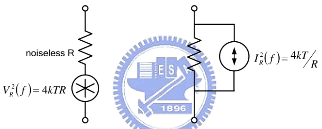
(2.13)where k, T, ,BW and R denote Boltzmann constant, temperature ,noise bandwidth and resistor. In the Fig. 2.6 illustrates the models.
noiseless R
( )
f kTR VR 4 2 =( )
f kT R IR 4 2 =Fig. 2.6 (a) A resistor thermal noise model with voltage source and (b) A resistor thermal noise model with current source
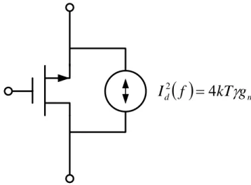
For a MOSFET, due to the resistive channel of a MOS transistor in active region, the thermal noise can be represented as
m 2
d
4
kT
g
I
=
•
γ
•
(2.14) where γ is a constant. γ =23 for the long channel transistors. The transistor( )
m df
kT
g
I
2=
4
γ
Fig. 2.7 Transistor thermal noise model
(vi) Flicker Noise
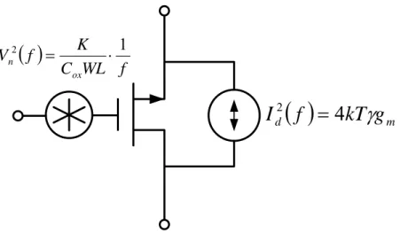
The flicker noise occurs at any junction, including metal-to-metal, metal-to-semiconductor, semiconductor-to-semiconductor, and conductivity fluctuations. The flicker noise arises mainly in amplifier circuits where there are numerous such contacts. At low frequency, flicker noise can be the dominant component, but it drops below thermal noise at higher frequency. The flicker noise spectral density is inversely proportional to frequency, so it is also called “1/f noise”. The phenomenon introduces the noise in the drain current and it can be modeled by a serial voltage source with the gate. Thus, larger device size introduces less flicker noise. It is common to use hundred or thousand micrometer square of devices in low-noise applications. The noise mode of transistor is shown in Fig. 2.8
( )
m df
kT
g
I
2=
4
γ
( )
f WL C K f V ox n 1 2 = ⋅Fig. 2.8 Noise model, including flicker noise voltage source and thermal noise current source.
f
1
WL
C
K
V
ox 2 ker fli=
•
(2.15)where C is the gate capacitance per unit area, W is the width of the transistor, L is ox
the length of the transistor, and K is the process-dependent constant on the order of F
V2
25
10− .
Figure 2.9 shows the noise power spectrum. There is an intersection point between flicker noise and thermal noise. It is called “corner frequency” or “1/f noise corner”. Frequency f Flicker noise -10dB/dec 1/f noise corner Thermal noise
( )
f VnThe total noise voltage of the transistor can be written as
.
g
1
3
2
kT
4
f
1
WL
C
K
V
m ox 2 ker fli & thermal⎟⎟
⎠
⎞
⎜⎜
⎝
⎛
•
+
•
=
(2.16) (5)Dark currentObserved when the subject image is not illuminated, dark current is an undesirable current that is integrated as dark charge at a charge storage node inside a pixel. The amount of dark charge is proportional to the integration time and is represented as follow and is also a function of temperature. The dark charge reduces the imager’s useable dynamic range because the full well capacity is limited. It also changes the output level that corresponds to “dark” (no illumination). Therefore, the dark level should be clamped to provide a reference
q
t
I
q
Q
N
dark dark INTdark
=
=
(2.17)(6) Sensitivity
Sensitivity determines the output signal of an image sensor illuminated by a certain light level within the specific integration time. The sensitivity is defined as the amount of photocurrent Iphoto produced when a unit of light power Plight is incident on
a material. It is given by light photo
/
P
I
y
Sensitivit
=
(2.18)The quantum efficiency is defined as the ratio of the number of generated photo carriers to the number of the input photons. In addition to enhancing sensitivity, the lens helps reduce crosstalk between pixels caused by minority carrier diffusion in CMOS image sensors. Conceptually, sensitivity is similar to spectral response in the sense that both parameters represent how the image sensors respond to light. In fact, sensitivity can be derived from spectral response if the spectral energy distribution of the illumination is known. For high sensitivity design, we can get high image quality.
(7) Signal to Noise (SNR)
The signal-to-noise ratio (SNR) is the ratio between the signal and the noise at a given input level. For SNR, the noise, nread, is the total temporal noise at the signal
level Nsignal. When the read noise is dominant in the total noise, SNR is given by
⎟⎟
⎠
⎞
⎜⎜
⎝
⎛
⋅
=
read signaln
N
log
20
SNR
(2.19)This term is considered a measure for high sensitivity of the image sensor when the entire illumination range from dark to light is readied.
2.2
Literature Review for Wide Dynamic Range Image Sensor
In this section presents a wide dynamic range for CMOS image sensor. It has been an important issue on photography whether in traditional camera or digital camera, which the ability to transform illumination of maximum and minimum light. On film’s angle, they define this ability in ISO grade. On digital camera’s angle, it can be define as dynamic range as (2.1).
Dynamic range of CMOS image sensor is especially the case, since their read noise and dark signal non-uniformity are typically larger than CCDs. For reference, standard CMOS image sensors have a dynamic range of 40–60 dB, CCDs around 60–70 dB, while the human eye exceeds 90 dB by some measures. In contrast, natural scenes often exhibit greater than 100 dB of dynamic range. To solve this problem, several dynamic range extension techniques such as well-capacity adjusting [26], multiple capture [27], time-to-saturation [28], and self-reset [29] have been proposed. These techniques extend dynamic range at the high illumination by increasing. In multiple capture and time-to-saturation, this is achieved by adapting each pixel’s integration time to its photocurrent value, while in self-reset the effective well capacity is increased by “recycling” the well. To perform these functions, most of these schemes require per-pixel processing. We would introduce some of them on the following sections
2.2.1 Wide Intrascene Dynamic Range CMOS APS Using Dual Sampling
O. Y. Petch. et al. proposed a wide intrascene dynamic tange CMOS APS using dual sampling in 1997[25]. The architecture of the new wide intrascene dynamic range approach is shown in Fig. 2.10. In this architecture, a second column signal processing chain circuit has been added to the upper part of the sensor. As before, row is selected for readout and copied into the lower capacitor bank. Row is reset in the process. However, immediately following, row is selected and copied into the upper capacitor bank. Row is also reset as a consequence of being copied. Both capacitor banks are then scanned for readout. With the difference integration time, which T1,int is the longer one and T2,int is the shorter one, the dynamic range capability is extended by the factor (T1,int / T2,int). This architecture helps not only extend dynamic range and also help to raise the signal to noise ratio. However, the limitation of this architecture should save large of image data into memories; it would take much longer time and large amount of memories to processing. It is hard to be used on movement application like video stream.
2.2.2 A CMOS Image Sensor with wide dynamic range pixelsand
column-parallel digital output
S. J. Decker. et al. proposed a CMOS imaging array with wide dynamic range pixels and column parallel digital output in 1998[21]. The principle of this architecture is to vary maximum value to save electron on photodiode. Except the weak illumination, it use lateral overflow to achieve non-linear wide dynamic range effect. Schematics for the pixel are shown in Fig. 2.11(a). The charge spill gate M3 increases sensitivity of the pixel by acting as a common gate amplifier that photocurrent flows into the low-impedance source node and is discharged into the high-impedance drain. The source follower Ml buffers the pixel from the large column line capacitance. The row-select device M2 connects the source follower output to the column line when the row is read out. The lateral overflow gate M4 increases pixel dynamic range. M4 gate voltage b(t) establishes a potential barrier to electron flow. As photo charge accumulates on the charge sense node, its charge level rises. If it exceeds the barrier level, the excess charge flows to the drain. Dynamic range is increased by decreasing b(t) over the integration period, as shown in Fig. 2.11(b). For low illumination, the integrated charge is unaffected by the barrier, so the pixel retains all of the photo charge. For high illumination, photocurrent spills into the drain between t1 and t2, and between t3 and t4. This reduces the final integrated charge, as shown by the difference between the dashed and solid lines. As illumination increases, a greater proportion of the photocurrent is diverted to the drain. Depending on the size, number, and timing of the steps in b(t), any arbitrary compression characteristic (final integrated charge vs. illumination) is approximated.
(a) (b)
Fig. 2.11 (a) Capacitance modulation pixel circuit and (b) Signal value versus capacitance modulation micro-array scanner system. [21]
2.2.3 A CMOS image sensor with ultra wide dynamic range
floating-point pixel-level
D. Yang. et al. proposed a CMOS image sensor with ultra wide dynamic range floating-point pixel-level in 1999[22].Ones method to embedded pixel level ADC and sampling at exponentially increasing exposure times, such as T, 2T, …, 2kT. Fig. 2.12(a) demonstrates the pixel circuit and column amplifier. To achieve acceptably small pixel size, each ADC, which is bit serial, is multiplexed among four neighboring pixels and generated by performing a set of comparisons between the pixel values and a monotonically increasing staircase RAMP signal. On the certain time, which N5 signal is equal RAMP one, the inversion signal would force BITX signal stay in the word transferring transistor to decide 1 bit data, and the Gray Code would be set up as the transferring reference. With different slope of RAMP, and m-bit serial A-D conversion k+1 times, they can get the higher resolution on digital data. Fig. 2.12(b) shows the m=2, k=2 with read serious signal in 4 bits (m + k). They transfer m-bits in period of T, and conversion another bit in 2T and 4T (2kT). This
kind of architecture is different as other instead of increasing input signal’s value. It uses the high resolution analog to digital conversion ability to analysis the weak illumination. Besides, if the illumination changed in saving period, the analog to digital conversion would have weakness on error.
(a) (b)
2.3 Literature Review for Biomedical CMOS Image Sensor
This section presents a particular and practical application of CMOS image sensor on developing a chip for detecting biomedical information. We will focus our research on biomedical subject information detection. It should be noticed that biomedical subject information is inspected and read by fluorescence signals. The target application of this proposal is to develop a biomedical CMOS image sensor chip for reading fluorescence signals.
2.3.1
Dual-image CMOS sensor for on-chip neural and DNA imaging applicationTakashi Tokuda et al. proposed an optical and potential dual-image CMOS sensor for on-chip neural and DNA (Deoxyribonucleic acid) imaging applications in 2006 [1]. Besides a CMOS image sensor which is capable to simultaneously sense an optical and an op-chip potential image was designed. The sensor was designed with target applications to sense neural activities and DNA spots in on-chip configuration. It designed compatibly configured light sensing pixel and potential sensing pixel. The basic characteristics of the potential sensing pixel are discussed and dual imaging functions are demonstrated.
The schematically for optical and potential image sensor is shown in Fig.2.13(a). In this design an optical and potential dual-image sensor which can capture optical and on-chip potential images simultaneously. The target applications of the proposed sensor are optical and potential image for neural image. The other schematically for
fluorescence + electric image sensor is shown in Fig.2.13(b). In this design an fluorescence + electric dual-image sensor which can capture fluorescence and on-chip potential images simultaneously. The target applications of the proposed sensor are fluorescence and electric for DNA micro-array.
Fig. 2.13 (a)On-chip optical + electric neural imaging and (b) on-chip fluorescence + electric DNA micro array sensing. [1]
2.3.2 A CMOS Bio-Sensor Array for Extracellular Recording of
Neural Activity
Björn Eversmann. et al. proposed A 128 x 128 CMOS bio-sensor array for extracellular recording of neural activity in 2003 [28]. The schematic and circuit structures of the biosensor array show in Fig. 2.14.
Fig. 2.14 The schematic cross section and circuit for biosensor array. [28]
Sensor arrays for non-invasive monitoring of neural signals from living cells are a key tool in neurosciences to study biological neural networks. Moreover, such sensor arrays open the way for fast and statistically significant cell-based pharma screening. The elementary neural signals (action potentials) are temporal peaks of the intracellular voltage. These action potentials are associated with ion currents through the cell membrane. When neurons within a grounded electrolyte are brought in intimate contact with an extra cellular electrode covered by a dielectric layer, a cleft of order of 50 nm between cell membrane and dielectric is obtained (Fig. 2.14). Membrane currents that flow through the cleft lead to a potential drop due to the resistance of the cleft. This voltage signal is coactively coupled to the electrode below. We connect this electrode to the gate of a MOSFET results in a modulation of the transistor's drain current. This extra cellular approach eliminates the need for an intracellular cell contact as is the case in classical invasive techniques.
2.3.3 A CMOS Image Sensor for DNA Microarrays
Samir Parikh et al. proposed A CMOS Image Sensor for DNA Micro-arrays in 2007 [2]. The component of the micro-array scanner structure is show in Fig. 2.15.
Fig. 2.15 Micro-array scanner system. [2]
The scanner consists of an excitation laser source, an emission filter and a CMOS chip that performs the light detection and quantification. The laser is used to excite an entire spot on a DNA micro-array. Moreover, the spot is aligned directly above a pixel on the CMOS chip, which is sized to be as large as the spot. Thus, the fluorescence emissions from an entire spot can be captured at once. In this prototype each spot on the DNA micro-array is individually scanned but this can be easily extended to parallel scanning with the fabrication of a multiple-pixel sensor and using a wider light source or a fast scanning laser. The emission filter is placed between the DNA micro-array and the image sensor to block the excitation photons from the laser source and allow the fluorescence emissions to reach the pixel. The system performance can be reduced by improving optical coupling, mechanical alignment, laser power supply noise, improved circuit noise and an increase in the conversion
gain. The CMOS sensor offers multiple-pixels for reduced scan time and an integrated analog-to-digital converter.
2.3.4 CMOS Bioluminescence Detection Lab-on-Chip
Helmy Eltoukhy et al. proposed a 0.18-μm CMOS bioluminescence detection lab-on-chip in 2006 [3].In this system describes a bioluminescence detection lab-on-chip consisting of a fiber-optic faceplate with immobilized luminescent reporters/probes that is directly coupled to an optical detection and processing CMOS system-on-chip (SoC) as show in Fig. 2.16. In addition to directly coupling and matching the assay site array to the photo detector array, this low light detection is achieved by a number of techniques, including the use of very low dark current photo detectors, low-noise differential circuits, high-resolution analog-to-digital conversion, background subtraction, correlated multiple sampling, and multiple digitization and averaging to reduce read noise. Electrical and optical characterization results as well as preliminary biological testing results are shown in this system.
The system test method was used in order to ensure that each of the individual components would meet the targeted noise, linearity and functionality requirements. Furthermore, the test chip allowed us to characterize the photodiode specifications.
2.4 Summary
In this chapter, the theoretical background of CMOS image sensor and the applications of CMOS image sensor in biomedical subject detecting are reviewed and discussed. All the detecting methods and circuit improvements above have realized the biomedical applications. This application for perceiving biomedical subject information in our design framework is called the biomedical image sensor. In the new CMOS process and circuit technologies will be advanced greatly in wide dynamic range and high sensitivity of the biomedical image sensor. In an attempt to produce high performance biomedical image sensor, the framework of this research is designed and conducted.
Chapter 3
Biomedical CMOS Image Sensor
Architecture and Simulation Result
In this chapter, the structure of the proposed biomedical CMOS image sensor (BIOCIS) is presented. It introduces the design and consideration of the complete BIOCIS from every stage circuit design, simulation, and verification. The architecture of the BIOCIS is introduced in Section 3.1. Section 3.2 the system design methods of this sensor is described. In Section 3.3, the system performance result of the BIOCIS is introduced.
3.1 Wide Dynamic Range Biomedical CMOS Image Sensor Architecture
This study aims to develop a BIOCIS with wide dynamic range, high fill factor, digital control built in the system, and low noise. BIOCIS is applied to detect biomedical subject information. The 32 × 32 pixel array of BIOCIS is the mixed model signal design. BIOCIS is divided into analog and digital parts. The analog part is used to detect fluorescence source and amplify the weak amplitude biomedical image signals. The circuits include 4T-APS, bootstrap circuit, correlated double sample circuit, and fully differential folded cascode operation amplifier. As for the digital part, different clock phase is used to control sensing circuits and sampling
circuits. Digital part be composed of 1-to-32 demultiplexers, 64-to-1 multiplexers, and two counters. The system structure of the BIOCIS is shown in Fig. 3.1.
Fig. 3.1 The block of the BIOCIS.
3.2 Circuit Design
The 32 × 32 pixel array structure of BIOCIS is divided into the analog and digital parts. Fig. 3.1 given above is the analog part which contains APS circuit, correlated double sample (CDS) circuit, and a fully differential folded cascode operation amplifier. The other part is the digital control. This stage is a row decoder, a column decoder, and clock signal generator. First part senses light source and processes those signals. The digital part dominates all of the transistors in the BIOCIS.
3.2.1 4-Transistor Active Pixel Sensor
In this section, the 4-T APS structure is introduced. The 4-T APS contains a photodiode, a transfer transistor, a reset transistor, a source follower transistor, and row select transistor. Fig. 3.2 shows the pixel structure of the 4-T APS.
Fig. 3.2 The structure of the 4T-APS.
The operation procedure is organized as follows. First, the signal charge accumulates in the photodiode diode. It is assumed that in the initial stage of the procedure there is no accumulated charge in the photodiode diode; a condition of complete depletion is satisfied. Just before transferring the accumulated signal charge, the floating diffusion is reset by turning on the reset transistor. The reset value is read out for correlated double sampling (CDS) to turn on the select transistor. After the reset readout is completed, the signal charge accumulated in the photodiode diode is transferred to the floating diffusion by turning on the floating diffusion with a transfer transistor, following the readout of the signal by turning on the select transistor.
Repeating this process, the signal charge and reset charge are read out. It is noted that the reset charge can be read out just after the signal charge readout. The physical structure of 4-T APS is show in Fig. 3.3 [6]. It used p substrate/N+ junction structure for the pixel array.
Fig. 3.3 The physical structure of the 4-T APS. [6]
The value of simulation results is a direct function of the quality of the models used for the photodiode design. SPICE model of this photodiode is shown in Fig. 3.4 [11]. The static behavior is modeled by voltage-current relationship. The dynamic behavior is represented by photocurrent Ip, which is the sum of outside light energy. The shunt parasitic capacitance Cp signifies the total capacitance of the p and n regions on both side of the junction. During the exposure, the photodiode will generate photocurrent storage on parasitic capacitance. The longer the exposure lasts, the more photocurrent occurs.
Fig. 3.4 SPICE model of the photodiode. [11]
In general, the 4-T APS circuit uses Cadence tool manually. The layout structure of 4-T APS is shown in Fig. 3.5. It contains 1) a photodiode and 2) four transistors. In the photodiode part will effort quality for pixel array. It is noted that the substrate noise and outside photo electric effect. Two methods will improve the quality of this APS. One method is uses guard rings around the photodiode can defect substrate noise. The other method design high level metal layer is stacked the transistors in the 4-T APS. This design will reduce photo electric effect.
In our design, each pixel is 25μm wide by 25μm deep and total area of 625μm2. The sensing area of per pixel is 373.4216μm2. We are able to identify that fill factor equal to 59.75% from this equation (3.1).
% 75 . 59 % 100 area Pixel area Sensign Factor Fill ⎟× = ⎠ ⎞ ⎜ ⎝ ⎛ = (3.1)
With one period of the clock signal flow, the one APS active performance shows in Fig. 3.6.
Fig. 3.6 The clock flow of 4-T APS.
We will describe one APS’s operation steps as follow:
(1) Row MOS: When Row MOS is turn on. It selects this pixel cell to sense and charge in the BIOCIS.
(2) Reset MOS: When Reset MOS is turn on. It will reset the gate of SF MOS. Immediately after this, the reset level is sampled from the gate of SF MOS and stored in the column circuit pixel cell signal.
(3) Transfer MOS: When Transfer MOS is turn on. It allows charge on the photodiode to transfer to the gate of SF MOS. Once charge transfer is complete, this charge (the photodiode signal level plus the gate of source follower reset level) is measured and stored in the column circuit.
3.2.2 Bootstrap Circuit
In order to guarantee an adequately low switch on-resistance in a low voltage environment, the clock voltage, used to drive only Reset NMOS switches, is bootstrapped beyond the supply voltage range. Therefore, the voltage multiplier technique is implemented. It converts available voltage to a higher voltage. Fig. 3.6 is shown a booted clock driver [7].
Fig. 3.7 Booted circuit. [7]
The capacitors CC0 (Cdb0) and CC1 (Cdb1) are charged to VDD (=1.5V) via the cross-coupled transistors M1a0 (M1aa0) and M1a1 (M1aa1). When the input clock is high, the output voltage approaches VDD + Vthreshold (=2V). The output voltage does not actually reach VDD + Vthreshold (=2V) due to the charge sharing with the parasitic capacitances of the output. Capacitor CC1 (Cdb1) must be large enough to boost the gates of MOS transistors to reduce the effect of charge sharing. To decrease the potential for latch-up, the bulk of the PMOS M0 (M1a) is tied to an on-chip voltage improvement. The bulk of the PMOS switch is biased by the circuit shown in
Fig. 3.7.
Fig. 3.8 Bulk circuit. [7]
Fig. 3.9 The layout result of the bootstrap circuit.
The bootstrap circuit simulation result voltage is 2V shown in Fig. 3.10.
Fig. 3.10 Simulation result of the bootstrap circuit.
3.2.3 Correlated Double Sample Circuit
In this section, we introduce sample signal circuit in the BIOCIS. The photo charge is amplified in the pixel and transferred to the noise suppression circuit, which makes a peculiar but very important contribution to the image quality of the image sensors. As the temporal noise is diminished by pixel/signal chain improvements, residual fixed pattern noise (FPN) which is the output of the FPN suppression circuit must be much lower than the temporal noise. Voltage-domain source follower readout
is the most common readout scheme. The combination of a pixel source follower and a column CDS circuit is shown in Fig. 3.11 [8]. The CDS circuit which consists of a current source, five switches, and two storage capacitances. Although the circuit is relatively simple, its performance is affected by a voltage gain loss, threshold voltage variations of the clamp switches, and less common mode noise rejection. Using a switched capacitor amplifier and multiple SC stages are introduced in the following section.
Fig. 3.11 The architecture of the CDS. [8]
In the CDS circuit, we are in need of taking into account the switch issue because of occurrences of the transistor type, different performance [39]. Fig. 3.12(a) indicates three types of switches. The n-type switch and p-type switch will produce negative output signal (poor 0 or poor 1), whereas utilizing CMOS switch results in best performance (good 0 and good 1) for output signal. Fig. 3.12(b) describes the three types (NMOS switch, PMOS switch and CMOS switch) ON resistance as the input voltage are sweep form GND to VDD, assuming the output voltage closely follows. During Vout nearly 0V, the NMOS switch is operating linearly and PMOS switch is cut off. During Vout nearly VDD, the NMOS switch is cut off and PMOS switch is
operating linear. Between Vout ~ 0.5 to Vout ~ VDD, the CMOS switch transistors are linear. The effective ON resistance is the parallel combination of two resistances and is relatively constant across the full range of input voltage.
Fig. 3.12 (a)Output performance of the different types switch;(b) Resistance of the switch type (NMOS, PMOS, CMOS). [39]
In CDS circuit with CDS switch is shown in Fig. 3.13. Three switches adopt this type (sample signal transistor, sample reset transistor, and knoise transistor ) in CDS circuit.
Fig. 3.13 The system chooses transmission gate for CDS structure.
Fig. 3.14 The layout result of the CDS circuit.
With one period of the clock signal flow, the one CDS active performance shows in Fig. 3.6.
Fig. 3.15 The clock flow of CDS circuit.
We will describe one CDS’s operation steps as follow:
(1) Sample_Reset: When Sample_Reset is turn on. It will storage reset signal on C_rst.
(2) Sample_signal: When Sample_signal is turn on. It will storage reset signal on C_sig.
(3) M1a&M1b: When M1a&M1b are turn on. This step is sample signal to operation amplifier.
(7) Offset_kill1: When Offset_kill1 is turn on. This step is transfer signal to operation amplifier.
The post simulation result of the CDS output (Vcds) from 30pA to 300pA is shown in Fig. 3.16.
Fig. 3.16 Simulation results of CDS circuit output form 50pA to 300pA.
In all corners (TT, SS, SF, FS, FF), simulation results for CDS circuit output is shown in Fig. 3.17.
Fig. 3.17 All corners simulation results of CDS circuit output form 50pA to 300pA.
3.2.4 Fully Differential Folded Cascode Operation Amplifier
The BIOCIS output signal is extreme weak (near nanometer level). We will design the operation amplifier for CDS output ports. Amplifying output signal could be measured and observed with less effort. This amplifier features differential operation due to the differential output of CDS. The differential operation amplifier can reduce noise than the single end operation amplifier. Fully differential op amp has three principal topologies: folded cascade, telescopic cascade, and two-stage op amp. Those structures comparatively present important attributes of the op amp topology as shown in Table 2. The folded cascode type gets the highest grade in this table. The folded cascode type contributes to medium voltage gain, high speed, best stability, and the highest output swing. The results of the folded cascode type meet our expectations for BIOCIS.
Table 2 Comparison of various op amp topologies. [34]
The fully differential folded cascode operation amplifier structure includes 1).reference bias circuit, 2).common mode feedback circuit (CMFB), and 3).folded cascode circuit as shown in Fig. 3.18.
Fig. 3.18 A fully differential folded cascode operation amplifier.
The block one is a constant transconductance bias circuit. It has wide-swing cascade current mirrors and can provide four biasing points that are suitable for our requirements. The block two, on the other hand, uses a kind of continuous time configurations feedback application. The applied feedback determines the differential signal voltages, but does not affect the common mode voltage. It is therefore
necessary to add additional circuitry to determine the output common mode voltage and to control it to be equal to some specified voltage, usually about halfway between the power supply voltages. Last but not the least, the block three uses folded cascode circuit for this operation amplifier performance. Equations of the gain, the bandwidth, the out swing, and the slew rate of the fully differential folded cascode operation amplifier are derived as follows.
(
m4o4o5 m2o2o3)
1 m g r r //g r r g Gain= (3.2) L 1 m C g Width Band = (3.3) L 0 D C I Rate Slew = (3.4)In our design, the differential gain of the operation amplifier (Gain) is 56dB; phase margin (PM) is about 80 degrees, bandwidth (BW) over 100Mhz and power consumption lower than 0.7mW. In all corners (TT, SS, SF, FS, FF), simulation results for this operation amplifier is shown in Fig. 3.19.
All corners post-layout simulation parameters of the fully differential folded cascode operation amplifier are summarized in Table 3. The differential gain ranges between 51 to 57dB, and phase margin is about 80 degrees, bandwidth over 100Mhz, output swing over 0.6Vp-p, and power consumption of the opamp lower than
0.75mW.
Table 3 All corners simulation result of op amp.
3.2.5 Switched Capacitor Circuit
Differential clock phase is employed to control CDS circuit and operation amplifier. This structure as a switched capacitor circuit and is shown in Fig. 3.20.
Fig. 3.20 A switched capacitor circuit.
The switched capacitor circuit can be divided into two modes. One is the sample mode, differential input signal storage C_sig and C_rst which facilitate to turn on M1a and M1b as shown in Fig. 3.21. The clock flow in the switched capacitor circuit is similar: In the sample mode, the finite input offset voltage of the operation amplifier is sampled and stored across a capacitor. In the transfer mode, this error voltage is subtracted form the signal voltage by appropriate switching of the capacitors.
Fig. 3.21 In sample mode. [34]
The other is a transfer mode, an offset switch which turns on, store and then transfer signal to output port as shown in Fig. 3.22.
Fig. 3.22 In transfer mode. [34]
The use of the sample mode and the transfer mode enables us to calculate the actual operation amplifier gain. Use charge conversion method, we can get capacitors relationship between input capacitance of the operation amplifier and load capacitance. The voltage gain are derived as follows
1) A 1 ( V C ) A V (V C ) V (V C ) V -(V C V -A V let type, Single v out1 2 v out1 in1 1 out1 2 in1 1 v out1 + − = + => − = => × = + + + (3.5) 2 1 2 1 op 2 1 in out v C C C C 1 A 1 1 1 C C | V V | | A | type al Differenti ≈ ⎟⎟ ⎠ ⎞ ⎜⎜ ⎝ ⎛ + + • = = => (3.6)
In the voltage relationship, the C1 equal to C_sig, C_rst and the C2 equal to Cop1 and Cop2. The operation amplifier gain varies make no changes to the switch capacitor amplifier. We can choose capacitor size to realize system voltage gain.
The above description is the analog part which contains APS circuit, CDS circuit, and a fully differential folded cascode operation amplifier. With one period of the clock signal flow, the one cell sensor performance shows in Fig. 3.23.
Fig. 3.23 One pixel cell operation and clock signal flow per period. In this figure, we will describe operation steps as follow:
(1) M,Row_sel: When M,Row_sel is turn on. It selects this pixel cell to sense and charge in the BIOCIS.
(2) M,Boot: When M,Boot is turn on. It will reset the gate of source follower. Immediately after this, the reset level is sampled from the gate of source follower and stored in the column circuit pixel cell signal.
(3) M,Sample_rst: When M,Sample_rst is turn on. It will storage reset signal on C_rst. (4) M,Transfer: When M,Transfer is turn on. It allows charge on the photodiode to
transfer to the gate of source follower. Once charge transfer is complete, this charge (the photodiode signal level plus the gate of source follower reset level) is measured and stored in the column circuit.
(5) M,Sample_sig: When M,Sample_sig is turn on. It will storage reset signal on C_sig.
(6) M,1a&M,1b: When M,1a&M1b are turn on. This step is sample signal to operation amplifier. It’s the same as sample mode in Fig. 3.21.
(7) M,offset_kill1: When offset_kill1 is turn on. This step is transfer signal to operation amplifier. It’s the same as transfer mode in Fig. 3.22.
3.2.6 Row Decoder and Column Decoder
The decoders of the biomedical image senor (BIOCIS) will control the row and column. The senor array area is 32 × 32. Design row decoder and column decoder are in accordance with the array size. Design row decoder to control those transistors (transfer transistor, reset transistor, and row select transistor) in APS. Four transistors (sample signal transistor, sample reset transistor, offset transistor, and choose operation amplifier transistor) are included in CDS. We apply 1-to-32 demultiplexers to realize it. The block of decoder architecture is shown in Fig. 3.24. It comprises both 1-to-32 demultiplexer and 5 bit counter.
Fig. 3.24 Row decoder and column decoder.
1-to-32 demultiplexer which uses CMOS combination circuit to compose will be the first one to be presented [40]. The circuit of 1-to-32 demultiplexer is shown in Fig. 3.25. It is a circuit that receives information on a single line and transmits this information on one of 25 possible output line. The function acts like a demultiplexer if the input line is taken as a data input line and lines S0, S1, S2, S3 and S4 are taken as the selection lines. Logic function can be verified form the truth table of this demultiplexer. Secondly, the five bit counter design still use CMOS combination circuit to compose and it’s shown in Fig. 3.26. In this counter design with five D flip-flops connected in such a way to always be in the "toggle" mode, we need to determine how to connect the clock inputs in such a way so that each succeeding bit toggles when the bit before it transits from 1 to 0. The Q outputs of each flip-flop will serve as the respective binary bits of the final. Counter used flip-flops with positive-edge trigger, we could simply connect the clock input of each flip-flop to the Q output of the flip-flop before it, so that when the bit before it changes from a 1 to a 0, the "falling edge" of that signal would "clock" the next flip-flop to toggle the next bit. The structure of five bits counter is presented in Fig. 3.26.
Fig. 3.26 Five bits asynchronous counter structure.
The post simulation result of the 1 to 32 demultiplexer is shown as Fig. 3.27. Total select four counts output of the demultiplexer. The results are corrected form 1-to-32 demultiplexer.
The post simulation result of the five bit counter is shown as Fig. 3.24. Five bit counter circuit for 1-to-32 demultiplexer is put to use. In the next section, six bit counter will manipulate clock signal generator.
Fig. 3.28 Simulation result of the five bits counter.
3.2.7 Clock Signal Generator
In this section, we will discuss clock signal generator for the BIOCIS. The system needs seven clock phases to supply for row decoder and column decoder. APS must create three data to control those transistors (transfer transistor, reset transistor, and row select transistor). CDS makes four data to control the transistors (sample signal transistor, sample reset transistor, offset transistor, and choose operation amplifier transistor). All of the data signal can be separated into sixth-four parts. Design a 64-to-1 multiplexer to realize this generator. The block of clock signal
generator architecture is shown in Fig. 3.29. It includes both 64-to-1 multiplexer and 6 bit counter.
Clock Signal
(Data input)
64 to 1
Multiplexer
SS0 SS1 SS4 SS56 Bit Counter
Signal
Fig. 3.29 The architecture of the clock signal generator.
In order to 64-to-1 multiplexer, we use 9 counts 8-to-1 multiplexers to realize it. The circuit of 64-to-1 multiplexer is shown in Fig. 3.30 and a 8-to-1 multiplexer circuit is shown in Fig. 3.26. The multiplexer is a combination circuit that selects binary information for one of many input status and generator clock phase to output line. There are 26 input status and six selection lines whose bit combinations determine which input signal is selected. The input status has two states, the supply voltage represented high status and ground represented low status.
![Fig. 1.2 A block diagram of signal path for an image sensor. [4]](https://thumb-ap.123doks.com/thumbv2/9libinfo/8756918.207126/14.892.169.756.360.445/fig-block-diagram-signal-path-image-sensor.webp)
![Fig. 1.3 The spectral response of the Visible light and Florescence. [4]](https://thumb-ap.123doks.com/thumbv2/9libinfo/8756918.207126/15.892.161.732.119.443/fig-spectral-response-visible-light-florescence.webp)
![Fig. 2.1 The structures of CCD image sensor and CMOS image sensor. [4]](https://thumb-ap.123doks.com/thumbv2/9libinfo/8756918.207126/19.892.135.731.114.394/fig-structures-ccd-image-sensor-cmos-image-sensor.webp)
![Fig. 2.4 Photo carriers in the photodiode. [30]](https://thumb-ap.123doks.com/thumbv2/9libinfo/8756918.207126/22.892.153.743.276.713/fig-photo-carriers-photodiode.webp)
![Fig. 2.10 Scanning method of dual-sample, dual output imager architecture. [25]](https://thumb-ap.123doks.com/thumbv2/9libinfo/8756918.207126/34.892.253.640.759.1066/fig-scanning-method-dual-sample-output-imager-architecture.webp)
![Fig. 2.12 The luminescence detection lab-on-chip composed of two substrates. [22]](https://thumb-ap.123doks.com/thumbv2/9libinfo/8756918.207126/37.892.138.747.309.669/fig-luminescence-detection-lab-chip-composed-substrates.webp)
