國
立
交
通
大
學
電機學院光電工程學系
顯示科技研究所
碩 士 論 文
複晶矽薄膜電晶體之電性分析
與溫度效應之探討
Study on Electrical Analysis & Temperature Effect
of Polycrystalline Silicon Thin-Film Transistors
研 究 生:鍾宛芳
指導教授:劉柏村 博士
張鼎張 博士
複晶矽薄膜電晶體之電性分析與溫度效應之探討
Study on Electrical Analysis & Temperature Effect of
Polycrystalline Silicon Thin-Film Transistors
研 究 生:鍾宛芳 Student:Wan-Fang Chung
指導教授:劉柏村 博士 Advisor:Dr. Po-Tsun Liu
張鼎張 博士 Dr. Ting-Chang Chang
國 立 交 通 大 學
電機學院光電工程學系顯示科技研究所
碩 士 論 文
A Thesis
Submitted to Department of Photonics Institute of Display
College of Electrical and Computer Engineering National Chiao Tung University
in partial Fulfillment of the Requirements for the Degree of
Master in Display August 2007
Hsinchu, Taiwan, Republic of China
複晶矽薄膜電晶體之
電性分析與溫度效應之探討
研究生:鍾宛芳 指導教授:劉柏村 博士
張鼎張 博士
國立交通大學 電機學院
光電工程學系顯示科技研究所碩士班
Chinese Abstract
在此論文裡,我們將探討橫向結晶(Lateral-Growth Crystallization, LGC)與 準分子雷射結晶(Excimer Laser Crystallization, ELC)之 N 型複晶矽薄膜電晶體 在低溫下所衍生的效應,並進一步研究通道中主晶界(main-Grain Boundary, main-GB)對於薄膜電晶體的影響,在此分為三種:主晶界之方向垂直於通道並 位於通道中央(VGB)、平行於通道(PGB)與沒有晶界存在於通道中(NGB)之三種 元件。 我們亦研究準分子雷射結晶P 型通道複晶矽薄膜電晶體的可靠度。利用直 流操作來模擬低溫複晶矽薄膜電晶體在使用後的劣化情形,並對閘極施加不同 的電壓與操作在不同溫度下,試圖找出元件在劣化情況下的相關係數與其劣化 機制。除此之外,我們還探討元件在負偏壓下之溫度不穩定性(Negative Bias Temperature Instability, NBTI)的動態回復與尺寸效應。Study on Electrical Analysis & Temperature Effect
of Polycrystalline Silicon Thin-Film Transistors
Student : Wan-Fang Chung Advisor : Dr. Po-Tsun Liu
Dr. Ting-Chang Chang
Department of Photonics and Display Institute
College of Electrical and Computer Engineering
National Chiao Tung University
English Abstract
In this thesis, we investigate the effects of cryogenic temperature and the main-Grain Boundary (main-GB) orientation in the channel region of N-type polycrystalline silicon thin film transistors (N-type poly-Si TFTs) fabricated by the Lateral-Growth Crystallization (LGC) and Excimer Laser Crystallization (ELC). Dividing the thin film transistors fabricated by lateral-growth crystallization into three kinds further. Described as follows: (1)The orientation of the main-GB is perpendicular to the channel and lie in the middle of the channel, abbreviated VGB. (2)The orientation of the main-GB is parallel with the channel, abbreviated PGB. (3)Without main-GB exists in the channel region, so called NGB.
We also study the reliability of p-type polycrystalline silicon thin film transistors (P-type poly-Si TFTs) fabricated by the ELC method. We utilize DC stress to simulate the operation of P-type poly-Si TFTs and observe the degradation degree. Then, adding the different gate bias and operating under various temperature, try to find the coefficients concerned with degradation and its mechanism of the TFTs. Additionally, we also research the dynamic recovery and dimensional effects under Negative Bias Temperature Instability, abbreviated the NBTI.
Contents
Chinese Abstract...i
English Abstract...ii
Contents... iii
Figure Captions...iv
Table Captions...vi
Chapter 1 Introduction...1
1.1 General Background...1
1.1.1 Overview of Low Temperature Poly-Silicon Thin-Film Transistors ...1
1.1.2 Negative Bias Temperature Instability in MOSFETs ...5
1.2 Motivation...7
1.3 Organization of This Thesis ...8
Chapter 2 Fabrication and Characterization ...10
2.1 Technology of Crystallization ...10
2.2 Fabrication Process of Poly-Si TFTs ...13
2.3 Introduction of Instruments...15
2.3.1 Cryogenics System – TTP-6 Probe Station (TTP)...15
2.3.2 Set up Instruments for Current-Voltage (I-V) Measurement 16 2.4 Methods of Device Parameter Extraction...16
Chapter 3 Results & Discussion...20
3.1 Influence of Temperature Effects on LTPS TFTs...20
3.1.1 The Lightly Doped Drain (LDD) Effects ...20
3.1.2 The Grain Boundary Effects...24
3.2 Negative Bias Temperature Instability in LTPS TFTs ...25
3.2.1 Dynamic Recovery in NBTI ...25
3.2.2 Characteristics of Negative Bias Temperature Instability ...27
3.2.3 Dimension Effect ...32
Chapter 4 Conclusion ...34
4.1 Temperature Effects...34
4.2 Negative Bias Temperature Instability...34
Reference...36
Figures...43
Figure Captions
Chapter 1 Introduction
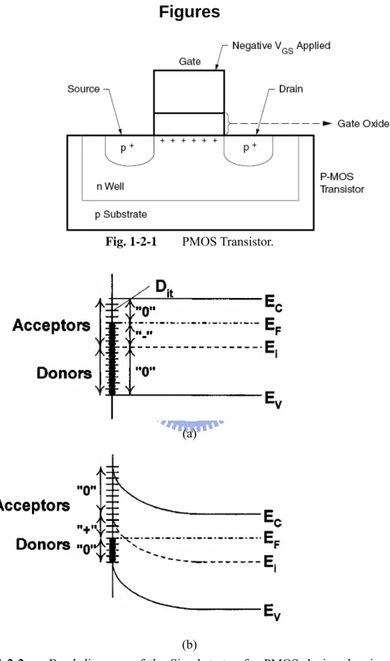
Fig. 1-2-1 PMOS Transistor.
Fig. 1-2-2 Band diagrams of the Si substrate of a PMOS device showing the
occupancy of interface traps and the various charge polarities for a
p-substrate with (a) negative interface trap charge at flatband and (b)
positive interface trap charge at inversion.
Fig. 1-2-3 Schematic representation of the Si/SiO2 interface, showing the
dynamic of degradation mechanism due to the hole for negative bias temperature instability.
Chapter 2 Fabrication and Characterization
Fig. 2-1-1 Process scheme of lateral-growth crystallized technology.
Fig. 2-2-1 The top-gated structure that the gate overlaps the source/drain 1μm of
low temperature polycrystalline N-type silicon thin film transistors manufactured by the lateral-crystallized process.
Fig. 2-2-2 The top-gated structure having the lightly doped drain (LDD)
structure of low temperature polycrystalline N-type silicon thin film transistors produced the lateral-crystallized process.
Fig. 2-2-3 The top view of a high-resolution scanning electron microscopy
(SEM) image of lateral-crystallized laser annealed poly-Si film. The continuous grain boundary is called the main-GB and the discontinuous and random grain boundary is named the sub-GB.
Fig. 2-2-4 Diagram of VGB-TFT, NGB-TFT, PGB-TFT.
Fig. 2-2-5 The top-gated structure makes use of self-aligned method of low
temperature polycrystalline P-type silicon thin film transistors produced by the lateral-growth crystallized process.
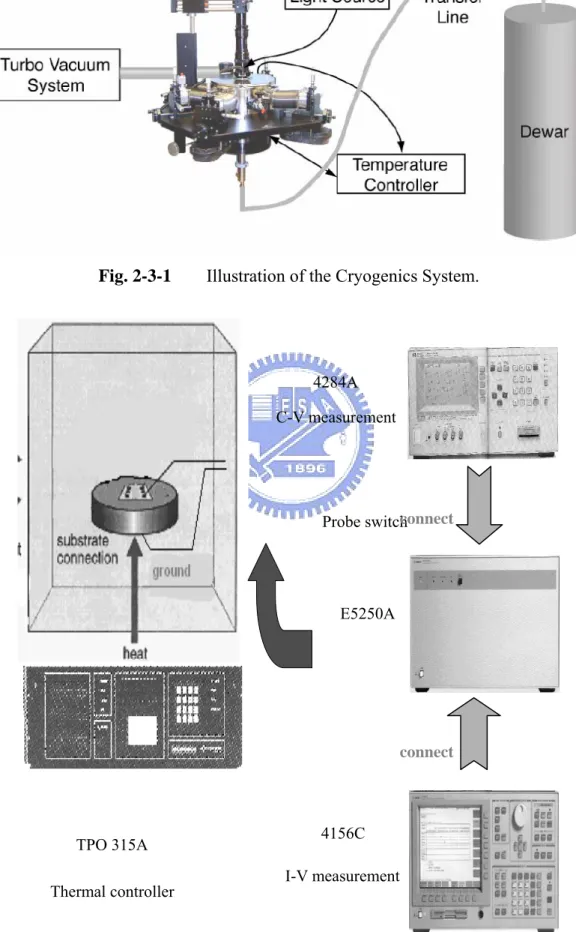
Fig. 2-3-1 Illustration of the Cryogenics System. Fig. 2-3-2 I-V/C-V instruments set up in the laboratory.
Fig. 2-3-3 The stress setup of the low temperature polycrystalline silicon thin
film transistors (the gate was given a constant bias and the drain and the source were grounded).
Fig. 2-4-1 Plotting of
(
)
ln D G FB I V V ⎛ ⎞ ⎜ ⎟ ⎜ − ⎟ ⎝ ⎠ versus(
)
2 FB G V −V − .Chapter 3 Results & Discussion
Fig. 3-1-1 The (a) ID-VG relations and (b) transconductance, gm, of poly-Si TFT
at the temperatures from -200℃ to 100℃.
Fig. 3-1-2 Two types of scatterings in MOSFET devices, including impurity
scattering and the phonon scattering.
Fig. 3-1-3 The ID-VG relations of the ELA non-LDD TFT at the temperatures
from -200℃ to 100℃, where the ID is the linear scale.
Fig. 3-1-4 The ID-VG relations of the (a) LDD and (b) non-LDD of ELA TFTs at
the temperatures from -200℃ to 100℃.
Fig. 3-1-5 The Gm-VG relations of the (a) LDD and (b) non-LDD of ELA TFTs
at the temperatures from -200℃ to 100℃.
Fig. 3-1-6 The sheet resistances of phosphorous (a) lightly-doped and (b)
heavily-doped poly-Si film at the temperatures from 50K to 300K.
Fig. 3-1-7 The dynamic and number of the free carriers of the lightly-doped Si
film at (a) High Temperature and (b) Low Temperature from the viewpoint of band-diagram.
Fig. 3-1-8 The LDD layers extended out the gate overlap region behave as the
temperature-dependent resistors and series connecting with the gate control region.
Fig. 3-1-9 ΔVth as a function of temperature of the (a) LDD and (b) non-LDD
TFTs.
Fig. 3-1-10 ΔμFE as a function of temperature of the (a) LDD and (b) non-LDD
TFTs.
Fig. 3-2-1 ΔVth as a function of stress time of the TFT suffered 1000sec stress at
25°C under the stress voltages VG= -15V and the removal of stress
revealing the recovery phenomenon.
Fig. 3-2-2 Schematic diagram of NBTI stress setup for the p-type ELA TFT.
The stress temperature was performed from 25 to 150°C, and the stress gate voltage was applied in the range of from −15 to −25V
with the source and drain grounded.
Fig. 3-2-3 The (a) transfer characteristics and (b) output characteristics of the
TFT before and after 1000sec NBTI stress at 125°C with the stress voltage is -25 V.
Fig. 3-2-4 Dependence of the threshold-voltage shift on the (a) stress time, (b)
stress temperature, and (c) stress voltage under various stress conditions.
Fig. 3-2-5 Grain boundary trap-state density extraction of the TFT before and
Fig. 3-2-6 Dependence of the grain boundary trap-state generation on the (a)
stress time, (b) stress temperature, and (c) stress voltage under various stress conditions.
Fig. 3-2-7 Comparison of the parameters extracted from the threshold voltage
shift and the grain boundary trap-state generation.
Fig. 3-2-8 Correlation between the grain boundary trap-state generation and the
threshold voltage shift of the LTPS TFTs after NBTI stress.
Fig. 3-2-9 Correlation between the subthreshold swing degradation and the
threshold voltage shift of the LTPS TFTs after NBTI stress.
Fig. 3-2-10 Energy band diagram of the p-channel LTPS TFT under NBTI stress. Fig. 3-2-11 ΔVth as a function of stress time of the different length and fixed the
width=6μm of ELA TFTs suffered 3000sec stress at 125°C under the stress voltages VG=-30V.
Fig. 3-2-12 The relationship between the channel length and ΔVth after NBTI. Fig. 3-2-13 ΔVth as a function of stress time of the different width and fixed the
length=6μm of ELA TFTs suffered 3000sec stress at 125°C under the stress voltages VG=-30V.
Fig. 3-2-14 The relationship between the channel width and ΔVth after NBTI.
Table Captions
Table 1 The comparison of device degradation degree applied different gate
voltage under NBTI stress with no stress interruption.
Table 2 The comparison of device degradation degree applied different gate
Chapter 1 Introduction
1.1 General Background
1.1.1 Overview of Low Temperature Poly-Silicon Thin-Film
Transistors
Thin-film transistors (TFTs) have in the past ten years become the “rice” of the electronic flat panel industry, just as silicon chips were earlier called the “staple”, of the electronic computer revolution. A large number of giant factories today produce millions of displays each year, with each display involving several million thin-film transistors [1.1].
Recently, polycrystalline-silicon thin-film transistors (poly-Si TFTs) have been widely investigated for applications such as active-matrix liquid-crystal displays (AMLCDs), organic light-emitting displays (OLEDs), and three-dimensional (3D) integrated circuits [1.2]-[1.4]. Besides large area displays, poly-Si TFTs have been applied to some memory devices like dynamic random access memories (DRAMs), static random access memories (SRAMs), electrical programming read only memories (EPROM),electrical erasable programming read only memories (EEPROMs). Poly-Si TFTs are also very potential to be used on devices such as linear image sensors, thermal printer heads, photo-detector amplifier, scanner, and neutral networks
[1.5]-[1.12]. In small size AMLCD application, such as the projector, which must be
high resolution and small size to lessen the cost associated with the projection optical system and keep the graphic quality. Additionally, poly-Si TFTs also play the role of light shutters in projection display. The higher durability against luminance and heat is needed since those devices are put adjacent to a high-power lamp. As a result, the application in AMLCDs is the major reason to improve the poly-Si TFTs technology rapidly. Undoubtedly, poly-Si TFT technology is the most promising approach.
The manufacture of polycrystalline silicon thin film transistors (poly-Si TFTs) embraces numerous steps commonly encountered in MOSFET fabrication for integrated circuits. Despite the similarities, however, a number of key differences exist. These differences emerge primarily from the fact that the substrate of TFTs is no longer a single-crystal silicon wafer, but rather a heat-sensitive material such as glass. In MOSFET fabrication, poly-silicon is usually prepared by LPCVD and then annealed above 900°C, namely, SPC (Solid Phase Crystallization) method. Unlike MOSFET devices, the TFT active layer needs to be formed on such amorphous host material and the temperature of all associated process has to be districted within the allowable range prescribed by the materials characteristics of the substrate. For current display-glass substrates, maximum processing temperature needs to be kept below 650°C. Even after considering possible exceptions to this maximum temperature such as RTA, the temperature range for fabrication on glass is severely constrained with respect to that on silicon. This limitation affects critical process steps, such as the gate-insulator formation and the activation of the doped regions of the device. These processes have to be reconsidered and optimized for TFT fabrication on glass. Hence, low temperature polysilicon (LTPS) technology is the novel technology specific for the flat panel display manufacture. Now, there are several ways to prepare the LTPS film on glass or plastic substrate: Metal-Induced Crystallization (MIC), Excimer Laser Crystallization (ELC), and Sequential Lateral Solidification (SLS), etc. Because of the methods mentioned above, the manufacturing technologies of poly-Si TFTs can lower the maximum process temperature enabling the use of low-quality glass and therefore reduce production cost [1.8].
Thin-Film Transistors (TFTs) with better performance will be essential to the next generation of mobile displays, since not only the pixel array but functional circuits, such as controllers, drivers, and so on, will be integrated on the same glass
substrate or plastic substrate. The possibility of these seems to represent a major advantage of the polysilicon technology over the amorphous silicon, because the mobility of poly-Si TFTs is usually larger than that of the a-Si TFTs. For poly-Si TFTs,
a mobility value larger than 50 cm2/V-sec is easily achieved by current technology, that is enough to used as peripheral driving circuits and bring the era of system-on-glass (SOG). The displays will require TFTs that minimize the power consumption and the maintenance, and to reduce manufacturing costs, and thus low threshold voltage, a steep subthreshold slope (S-value), high field-effect mobility. In addition, due to the higher mobility of poly-Si TFTs , the dimension of the poly-Si TFTs can be made smaller compared to that of amorphous Si TFTs for high density, high resolution AMLCDs.
Enhancing the performance of poly-Si thin-film transistors, as well as improve their reliability to realize various applications mentioned above. Recently, the performance gap between poly-Si TFTs and single-crystalline silicon devices has become smaller as a result of the advancement in poly-Si crystallization techniques. In comparing poly-silicon devices with their single-crystal counterparts, the major difference arises because of the presence of grain boundaries in the poly-Si. There are high density trap states in the grains and along the grain boundaries, and the electrical activity of the charge-trapping centers profoundly affects the electrical characteristics of poly-Si TFTs. Large amount of defects serving as trap states locate in the disordered grain boundary regions to degrade the ON current seriously [1.13]. In short, the grain boundary influences the TFT characteristics, and the typical device characteristics of TFTs will be poor compared with the devices fabricated on single crystal silicon film.
Moreover, the relatively large leakage current is one of the most important issues of poly-Si TFTs under OFF-state operation [1.14], [1.15]. The dominant mechanism of the leakage current in poly-Si TFTs is field emission via grain boundary traps due to the high electric field near the drain junction [1.15]-[1.18]. Consequently, there are two ways to reduce leakage current: one is to reduce grain-boundary trap density and the other is to alleviate the electric field near the drain side.
To overcome this inherent disadvantage of poly-Si films, many researches have been focused on modifying or eliminating these grain boundary traps. Hydrogenation is a method for reducing the trap density in poly-Si films [1.19]-[1.21]. As the number of trapped carriers decreases, the potential barrier associated with the grain boundary also decreases. The defect-state density can also reduced by improving the crystallinity of poly-Si film with techniques such as laser annealing [1.22]-[1.23] and solid-phase crystallization [1.24], [1.25] to enlarge the grain size. For devices with smaller dimensions, the number of grain boundaries decreases since there are fewer grains within the channel region. Because the drain voltage drops on the depletion regions located at grain boundaries, a large electric field will exist in small dimension TFTs and make the drain current increase dramatically due to the impact ionization. Hence, a drain offset region or lightly-doped drain region is used to suppress leakage current by decreasing drain electric field.
In summary, it is expected that the poly-Si TFTs will becomes more and more important in future technologies, especially when the 3-D circuit integration era is coming. More researches studying the related new technologies and the underlying mechanisms in poly-Si devices with shrinking dimensions are therefore worthy to be indulged in.
1.1.2 Negative Bias Temperature Instability in MOSFETs
With the advanced fabrication processes are utilized, the transistor dimensions have shrunk and the electric field applied to the gate oxide has increased. A gradual shift of threshold voltage (VT) over time is commonly observed in p-type MOSFETs.
This shift is caused by: voltage stress on the gate oxide, temperature. Known since 1961, this effect, an unwanted transistor behavior that is pervasive in all deep sub-micron designs, has become more severe with the advanced processes that use PMOS transistors.
NBTI occurs mainly in p-channel MOS devices stressed with negative gate
voltages or elevated temperatures which can produce NBTI, but a stronger and faster effect is produced by their combined action. It manifests itself as absolute drain current ID, and transconductance gm, decrease and absolute off current Ioff, and
threshold voltage VT increase. It also leads to timing shifts and potential circuit
failure due to increased spreads in signal arrival in logic circuits. Typical stress temperatures lie in the 100~250°C range with oxide electric fields typically below 6 MV/cm. Such fields and temperatures are typically encountered during burn in, but are also approached in high performance ICs during routine operation.
The smaller transistors have incremental potential for interface traps in PMOS transistors during prolonged times of negative bias stress. An interface trap is created when a negative voltage is applied to the gate of a PMOS device for a prolonged time (see Figure 1-2-1). An interface trap is located near the Si/SiO2
boundary where holes (positive charge) can get stuck, and in doing so, they shift the
threshold voltage. This hole trapping creates interface states as well as fixed charges. Both are positive charges and result in a negative shift of threshold voltage. This phenomenon is called PMOS Negative Bias Temperature Instability (NBTI). NMOS transistors are far less affected because interface states and fixed charges are of
opposite polarity and eventually cancel each other.
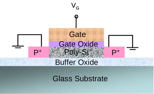
To perform an NBTI study of a PMOS transistor, a constant negative bias is applied to the gate electrode at high temperatures, with source, drain, and substrate grounded.
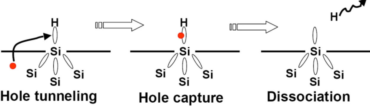
Interface traps at the SiO2/Si interface are acceptor-like in the upper half and
donor-like in the lower half of the band gap shown in Fig. 1-2-2(a). Hence, at flatband, where electrons occupy states below the Fermi energy, the states in the lower half of the band gap are neutral (designated by ‘‘0’’), being occupied donor states. Those between mid gap and the Fermi energy are negatively charged (designated by ‘‘-’’), being occupied acceptor states and those above EF are neutral
(unoccupied acceptors). For an inverted p-channel MOSFET, shown in Fig. 1-2-2(b),
the fraction of interface traps between mid gap and the Fermi level is now unoccupied donors, leading to positively charged interface traps (designated by ‘‘+’’). Hence interface traps in p-channel devices in inversion are positively charged,
leading to negative threshold voltage shifts [1.26]-[1.28].
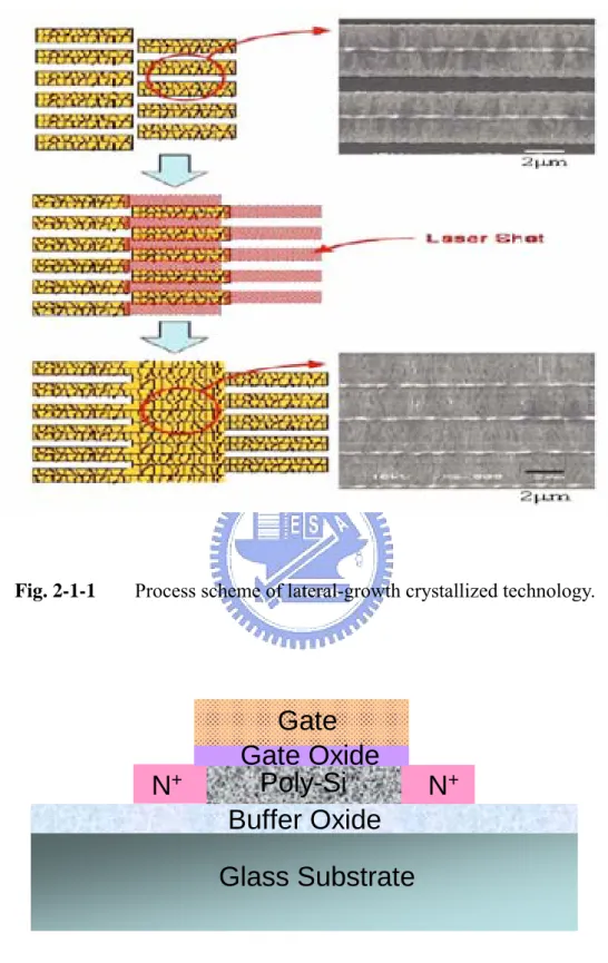
Consequently, we depicted the NBTI degradation mechanism in MOSFETs.
Fig. 1-2-3 shows that the Si dangling bonds at the poly-Si/SiO2 interface are
passivated by the hydrogen atoms initially, forming ≡Si−H bonds. During NBTI
stress, the hydrogen atoms at the poly-Si/SiO2 interface, being weakly bonded to the
Si atoms, react with the holes from the inversion layer and dissociate from the Si atoms. The hydrogen depassivation results in the generation of interface trap states (≡Si•) and the released hydrogen species from the interface diffuse or drift into the gate oxide and react with it, forming OH groups bounded to oxide Si atoms (≡Si−OH) and leaving positive fixed oxide charges (≡Si+) in the gate oxide. Finally, the hydrogen species diffuse in the gate oxide, becoming the reaction-limiting factor. We conclude that the generation of interface trap states and fixed oxide charges
during the NBTI stress contributes to the threshold-voltage shift and degrades the reliability of MOSFETs [1.29].
1.2 Motivation
Now, the large area electronics or the flat-panel displays comprised of poly-Si TFTs are used by peoples at the globe. Thus, the displays should keep the performances well at all kinds of the environments. In addition, we also expected that the poly-Si TFTs can be more widely used in astro-technology in the future. Temperature usually influences the characteristics of solid-devices, and its relative effects are important for the application of Poly-Si TFT technology. Therefore, the temperature effects on the n-type poly-Si TFT with/without LDD structure and the grain boundaries occurrence were investigated.
Poly-Si TFTs have also attracted much attention due to the possibility of practicing the integration of peripheral circuit and active matrix. From the viewpoint of fabrication-technology and as a long-term reliability concern, the stability of poly-Si TFTs is of significant importance [1.30]. In p-channel MOSFETs, negative bias temperature instability has been found to be an important reliability issue and extensively investigated. The NBTI degradation in MOSFETs is mainly attributed to the generation of interface trap states and fixed oxide charges, and it can be thermally and electrically activated [1.28], [1.31]-[1.32]. In poly-Si TFTs, as a result of the poor thermal conductivity of the glass substrate and higher operation voltage, we assume that the NBTI is more important in the reliability of poly-Si TFTs. Okuyama et al. have specified that the NBTI stress leads the performance
degradation in poly-Si TFTs as well as in MOSFETs [1.26]. However, the NBTI degradation has not been thoroughly studied in poly-Si TFTs, and the mechanism is
not well known. We also conjecture that the NBTI-degradation mechanism in poly-Si TFTs, due to the grain boundaries in the channel regions, may be different from that in MOSFETs. Some studies have pointed out that the NBTI stress on poly-Si TFTs may generate trap states in the grain boundaries; however, the correlation between the grain-boundary trap-state generation and the device degradation during NBTI stress in poly-Si TFTs has not been deeply investigated
[1.29].
1.3 Organization of This Thesis
The thesis is organized as following: in Chapter 2, introduction of poly-Si crystallization methods and the fabrication procedure of LTPS TFTs. Simultaneously, the instruments for cryogenics system and current-voltage (I-V) measurement will be introduced. Consequently, describing the methods of device parameter extraction. In Chapter 3, the experiment processes and conditions will be illustrated. The contents includes the cryogenics current-voltage (I-V) measurement with/without grain boundaries and grain boundary orientation and then study the reliability of p-channel polycrystalline silicon (poly-Si) thin film transistors (TFTs) under negative bias temperature instability stress. Following is the experimental results and discussions. The distinct phenomenon, including the conducting current and mobility, was found between the LDD and non-LDD TFTs due to the lightly doped drain under different operation temperature. However, the characteristics of grain boundary orientation in the lateral crystallized TFTs show no apparent differences. On the other hand, from the NBTI of p-channel TFTs, we proved that NBTI is important on the reliability of LTPS TFTs. We found that the device characteristics will be degraded after NBTI stress and can be thermally and electrically activated. Besides, we observed that the threshold-voltage shift is closely related to the
generation of grain-boundary trap states and interface trap states; we conclude that the NBTI degradation in LTPS TFTs is caused by the generation of fixed oxide charges, interface trap states, and grain-boundary trap states. In addition, a physical model is recommended and verified by the experimental results. In Chapter 4, concluding remarks and future works are presented.
Chapter 2 Fabrication and Characterization
2.1 Technology of Crystallization
Crystallization is the most important technology in the TFT fabrication process from the viewpoint of securing and enhancing the TFT performance due to the approach of crystallization dominates the crystallinity of poly-Si films. The low-temperature crystalline Si-based thin-film transistors (TFTs) have been fabricated on materials with polycrystalline microstructures. In order to make a process viable for use in manufacturing, the material quality must be optimized for performance, throughput, and uniformity. For poly-Si TFTs, the electrical properties of the device are limited by the existence of grain boundaries in the channel regions. Moreover, the channel mobility is limited by the potential barriers formed at the grain boundaries, which are the result of trapping states due to dangling bonds [2.1]. The grain boundaries in the poly-silicon material play a detrimental effect on the TFTs performance due to the presence of a high density of trapping states. The grain boundary effects on the device performance can be reduced by enlarging the grain size and, thus, reducing the number of grain boundaries within the channel of the TFTs. Therefore, it is essential that we reduce the number of defects in the TFT channel by reducing the occurrence of grain boundaries.
In order to improve the transistor characteristics, there has been a lot of research to enlarge the grain size and control grain boundary location and crystal orientation
[2.2]-[2.4]. Most poly-Si TFTs are fabricated using crystallized amorphous silicon
films. While many schemes for producing low temperature polycrystalline Si films have been developed such as solid phase crystallization (SPC), conventional excimer-laser crystallization (ELC) and Lateral-Growth Crystallization (LGC) is another way to obtain uniform TFTs with large grains and enhance high field-effect
mobility, none have been able to accommodate all of the requirements. We will introduce the excimer-laser crystallization (ELC) and Lateral-Growth Crystallization (LGC) in the following paragraphs, in this experiment we utilized.
Excimer-laser is a type of gas laser where lasing medium is composed of an inert atom and a halide atom (i.e., Cl, F) and the name excimer itself is an abbreviation of “excited dimmer,” meaning a diatomic excited molecule. Excimer-lasers feature wavelengths in the UV range of the spectrum that is suited to Si crystallization, for
a-Si absorbs very strongly in the UV range. Therefore, the energy in the incident laser
pulse is strongly absorbed within only the first few mono-layers of the film (i.e., within 60-100Å of the surface of the Si film), and this causes very rapid heating and melting to occur within the Si film. Excimer-laser crystallization (ELC) has attracted much research interest recently as a low-temperature processing method for the crystallization of a-Si films [2.5], [2.6] or for the enlargement of the polysilicon film grain size [2.7]. One of the important advantages of low-temperature polycrystalline silicon thin film transistor (LTPS-TFT) technology is the opportunity to make use of the low cost glass substrates due to the low temperature of the excimer laser annealing (ELA) process [2.8], [2.9]. The goal of these investigations was optimization of the ELC process to maximize the grain size of polysilicon films. The end products of these processes range from small-grained to large-grained polycrystalline Si films that unfortunately and invariably contain randomly located grain boundaries throughout the crystallized area.
Additionally, improvement in electrical properties of polycrystalline Si thin films can be achieved by reducing the number of grain-boundaries and by controlling their location within the channel region [2.10]. The Lateral-Growth Crystallization process is an excimer-laser projection-based scheme for crystallization of thin films on amorphous substrates. An excimer-laser-based crystallization technique that enables
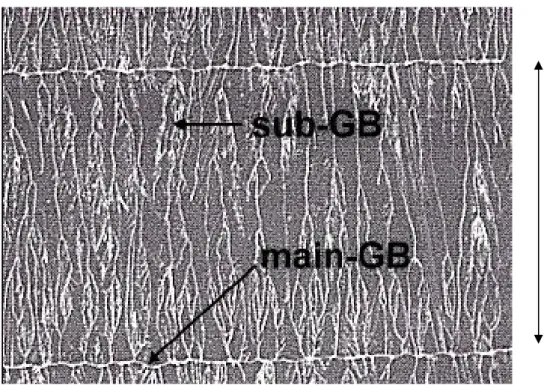
controlled periodic placement of high-angle grain boundaries has been developed in order to address the problems associated with the presence of defects within the material [2.11], [2.12]. In lateral-growth crystallization technique, using a mask of a long checker pattern and the repetition of laser irradiations translating the mask, the solidification succeeds to the previously grown grains, resulting in the formation of long grains, as shown in Figure 2-1-1. This method has been developed to achieve
this goal by controlling the location and orientation of grain boundaries or by eliminating grain boundaries in the channel region altogether. For example, the directional solidification form of lateral-growth crystallization technique produces material with long, roughly parallel grains and grain boundaries [2.13]-[2.14].
The Lateral-Growth Crystallization is a process that can effectively and efficiently produce either directionally solidified microstructures or location-controlled, single-crystal (i.e., grain-boundary-free) regions on Si films on SiO2. The method corresponds to the only demonstrated means for directly producing
such materials, without resorting to costly and size-limited SOI-derived approaches, on high-temperature-intolerant substrates, such as glass or plastic [2.10], [2.13]. This method can be used to readily produce a wide range of microstructures through manipulation of grain boundary placement within the crystallized material. This lateral crystallization scheme allows one to manipulate the resulting microstructure of the polycrystalline Si film to yield a wide range of material quality: from large defect-free single-crystal islands to uniform large-grained polycrystalline material
[2.15], [2.16]. After the lateral-crystallized process, thinning and planarization of the
Si surface was utilized to improve the uniformity and performance of the TFT devices. The lateral-growth crystallization, is compatible with low-temperature substrates, and yet produces a directionally solidified microstructure that consists of nonequiaxed
lateral-crystallized-processed Si films the best low-temperature-substrate-compatible TFT material that has been directly obtained to date [2.13].
More significant is the fact that the lateral-crystallized process possesses the potential for directly producing the ideal material for fabricating the highest quality TFT devices: large, location-controlled single-crystal Si regions (i.e., areas that are completely free of grain boundaries) on top of substrates that are intolerant of high processing temperatures. One of the main disadvantage to this process is the appearance of surface protrusions within the active channel region, which add to the non-uniformity of devices not only through scattering of the majority carriers, but also by limiting scaling of the gate oxide thickness. It is especially important to address this problem when scaling devices to improve the switching speeds of driver circuits that will be fabricated on large-area panels [2.17].
2.2 Fabrication Process of Poly-Si TFTs
In the thesis, the poly-Si TFTs we used are top-gated type and fabricated on glass substrate by low-temperature processes, regardless of the ELC and the lateral-crystallized processes.
The lateral-crystallized process is depicted as following. Buffer SiO2films and
90-nm-thick amorphous silicon films were deposited by plasma enhanced chemical vapor deposition (PECVD) on glass substrate, and subsequently, the films were dehydrogenated by furnace annealing. After dehydrogenation, the a-Si films were
crystallized by lateral-growth crystallized laser annealing process. The lateral-crystallized process is an excimer-laser projection-based scheme for crystallization of thin films on amorphous substrates. This method can be used to readily produce a wide range of microstructures through manipulation of grain
boundary placement within the crystallized material. Following the lateral-crystallized process, 100-nm-thick gate oxide was deposited by PECVD. MoW was sputtered as a gate electrode and phosphorous ion doping was used to form source and drain (S/D) regions. The overlap/LDD (Lightly Doped Drain) of N-type device between gate electrode and S/D junction is 1μm. The structure is shown in Fig. 2-2-1 and Fig.
2-2-2.
Fig. 2-2-3 shows the top view of a high-resolution scanning electron microscopy
(SEM) image of the lateral-growth crystallized laser annealed poly-Si film. It includes a domain region containing a mixture of plurality of crystals substantially parallel to the carrier body. The crystals may be columnar or capillary crystals. The grain boundaries present in the lateral-crystallized laser annealed poly-Si film can be divided into two types, named the main-GB and sub-GB, as labeled by the arrowhead in Figure 2-2-3. The width of each main-GB is about 100 nm and the space between main-GBs is approximately 3.5 μm. Figure 2-2-4 shows the tested devices that the main grain boundary is vertical to the channel and in the middle of the channel (VGB TFT), without main grain boundary in the channel (NGB TFT) and the main grain boundary parallel with the channel (PGB TFT).
Then, we introduce the ELA-TFT manufacturing process. 550-nm-thick buffer SiO2films were deposited by PECVD on glass substrate, and subsequently, undoped
amorphous-Si layers were deposited by low pressure chemical vapor deposition (LPCVD) at 550°C. The amorphous-Si films were recrystallized by excimer laser annealing (ELA) method. These recrystallized poly-Si films were then patterned into active region islands by transformer couple plasma (TCP) etching using the mixture of Cl2 and HBr. Following the ELA process, 100-nm-thick gate oxide was deposited
by PECVD using TEOS and O2 gases at 300°C. Al was sputtered as a gate electrode
The overlap/LDD (Light Doped Drain) of N-type device between gate electrode and S/D junction is 0.75 μm, and the process of P-type device is self-aligned. The structures are similar to the SLS-TFTs, shown in Fig. 2-2-1 ,Fig. 2-2-2 and Fig. 2-2-5.
2.3 Introduction of Instruments
We will separate this section into two parts. One is the brief introduction of the cryogenics; the other is concerned in the measurement setup.
2.3.1 Cryogenics System – TTP-6 Probe Station (TTP)
The system is illustrated in Figure 2-3-1. The photo shows the TTP with the microscope and camera installed. The remaining components necessary to run the system are connected to the TTP. To use the system, samples are placed inside the TTP chamber, the system is evacuated with the turbo vacuum system, and the sample is cooled with a cryogen. Probes are moved into place on the sample while observing with the microscope. Measurements of sample properties are then made via the probes. [2.18]
When the system is not used, the chamber needs to be kept the vacuum. We must vent the chamber with nitrogen gas to load a sample before measurement. After that, seal the chamber and evacuate it using turbo pump until the IG (ion gauge) readout on the vacuum system is 7.6 -5. Insert the both ends of the transfer line into a Dewar and the bayonet on the TTP, respectively, and set the desirable temperature on the temperature controller. Start to cool the sample down to the desirable lowest temperature and perform the experiment. We utilize microscope to view and make measurements of sample via the probes. Then, entering a set point on the temperature controller to warm the system, get back to the room temperature or even
high temperature. After accomplishing the experiment, we must make the chamber temperature at room temperature before venting it. Finally, unload the sample and keep the chamber at vacuum state.
2.3.2 Set up Instruments for Current-Voltage (I-V) Measurement
The electrical test setup of HP4156C semiconductor parameter analyzer is utilized in this experiment, illustrated in Figure 2-3-2, a probe station is situated inside a dark box. The ground probe station is furnished with an electrically isolated, water-cooled thermal chuck. The chuck is controlled by Temptronic TPO315A thermal controller, which can operate temperature from 25°C to 300°C. An Agilent 4156C precision semiconductor parameter analyzer can provide I-V measurement, bias for BTS, and quasi C-V measurement, etc. We employ the ICS (Interactive Characterization Software) to obtain the output and transfer characteristics, like VD-ID, VG-ID (Linear), VG-ID (saturation), and extract the typical semiconductor
parameters.
In order to investigate the effect of the DC gate-bias stress (i.e., the gate was given a constant voltage while the source and the drain were grounded) on the electrical parameters of excimer laser annealing (ELA) low temperature poly-silicon TFTs, the stress setup is shown in Figure 2-3-3.
2.4 Methods of Device Parameter Extraction
In this section, we will introduce the methods of typical parameter extraction such as the threshold voltage VT, subthreshold swing S.S, field-effect mobility
Several methods are used to determinate the threshold voltage, VT , which is the most important parameter of the semiconductor devices. The method to determinate the threshold voltage in this thesis is the constant drain current method,
the voltage at a specific normalized drain current NID is taken as the threshold
voltage. This technique is adopted in most studies of TFTs. It can give a threshold voltage close to that obtained by the complex linear extrapolation method. Typically, the specific normalized current NID = ID/(W/L) is defined at 10nA for VD operated in
linear region and 100nA for VD operated in saturation region, to extract the threshold
voltage of TFTs in most papers.
The subthreshold swing S.S (V/dec) is a significant parameter to describe the control ability of gate bias toward drain current and the efficiency of the switch turning on and off. It is defined as the amount of gate voltage required to increase/decrease drain current by one order of magnitude. It should be independent of drain voltage and gate voltage. However, in reality, the subthreshold swing might increase with drain voltage due to the short-channel effects such as charge sharing, avalanche multiplication, and punch through-like effects. It is also related to the gate voltage due to some undesirable factors such as serial resistance and interface state. In this experiment, the subthreshold swing is defined as one-second of the gate voltage required to decrease the threshold current by two orders of magnitude. The threshold current is specified to be the drain current when the gate voltage is equal to the threshold voltage.
The field-effect mobility (μFE) is determined from the transconductance gm at
low drain voltage (linear region). The transfer characteristics of poly-Si TFTs are similar to those of conventional MOSFETs, ignoring any other non-ideal effect and assuming the electric field in the channel is uniform, so the first order I-V relationship in the bulk Si MOSFETs can be applied to the poly-Si TFTs, which can
be expressed as 2 1 [( ) ] 2 D FE ox G T D D W I C V V V V L μ = − − (2-1) where Cox is the gate oxide capacitance per unit area
W is channel width L is channel length
VT is the threshold voltage.
If VD is much smaller than (VG-VT) (i.e., VD << VG-VT ) and VG > VT, the drain
current can be approximated as:
( ) D FE ox G T D W I C V V V L μ = − (2-2) The transconductance is defined as
D FE ox const V G D m V L WC V I g D =
μ
∂ ∂ = = . (2-3)Therefore, the field-effect mobility can be obtained by gm D ox FE WV C L = μ (2-4) The mobility value was taken from Equation (2-4) with maximumμFE.
The extraction method of the trap density Nt is following. From the Seto’s
model, the grain boundary potential barrier height VB can be expressed by the
following equation 2 2 2 2 8 t B t s s N qN qn V n n ε ε ⎛ ⎞ = ⎜ ⎟ = ⎝ ⎠ (2-5)
where VB is the grain boundary potential barrier height
n is the carrier concentration
Nt is the grain boundary trap density
The grain boundary potential barrier height VB is related to the carrier
Based on this consideration, the amount of trap state density Nt can be extracted
from the current-voltage characteristics of poly-Si TFTs. As proposed by Levinson
et al. [1.14], the I-V characteristics including the trap density can be obtained by the
following equation
(
)
(
)
3 2 0 exp 8 t ch D ox G TH D s ox G TH q N t W I C V V V L kT C μ ε ⎛ ⎞ = − ⎜⎜− − ⎝ V V ⎠⎟⎟ (2-6) This equation had been further corrected by Proano et al. by considering themobility under low gate bias [2.19]. It is found that the behavior of carrier mobility under low gate bias can be expressed more correctly by using the flat-band voltage VFB instead of the threshold voltage VTH. Moreover, a better approximation for
channel thickness tch in an undoped material is given by defining the channel
thickness as the thickness at which 80 percent of the total charge resides. Therefore, by solving the Poisson’s equation, the channel thickness is given by
(
)
8 s ox ch ox G FB kT t qC V V ε ε = − (2-7) The drain current of poly-Si TFTs then should be expressed as2 2 0 ( ) exp 2( ) ox t s D ox G FB D ox G FB q N W I C V V V L C V ε ε μ ⎛ ⎞ ⎜ ⎟ ⎜ = − − − ⎜ ⎟ ⎜ ⎟ ⎝ ⎠ 2 V ⎟
)
)
(2-8)The effective trap state density then can be obtained from the slope of the curve versus
(
(
ln⎡⎣ID/ VG−VFB ⎤⎦ 2
G FB
V −V − as in Figure 2-4-1 and we can calculate the slope from it. The grain boundary trap-state density can be determined from the square root of the slope directly, expressed by the simplified equation below.
ox trap C N S q = lope (2-9)
Chapter 3 Results & Discussion
3.1 Influence of Temperature Effects on LTPS TFTs
In this experiment, we have two kinds of sample – Excimer Laser Annealing (ELA) and Lateral-Growth Crystallized (LGC) TFTs. Divide the N-type sample into four parts: (A)VGB, (B)NGB, (C)PGB, and (D)ELA. We take the ELA TFT as the standard TFT, comparison of the LGC-TFTs. The VGB and PGB represent that the orientation of main grain boundary is vertical to and parallel with the channel, respectively. The NGB means that without main grain boundary in the channel region, diagram is shown in Fig. 2-2-4. Besides, the four parts all contain the LDD (Lightly Doped Drain) and non-LDD devices.
The experimental procedure is depicted below. Load the samples to the cryogenics system and cool the sample down to the desirable measurement temperature. Measure the I-V characteristics using the HP4156C semiconductor parameter analyzer. We measure VG-ID in linear regime (VD=0.1V) at -200°C,
-100°C, -50°C, 0°C, 27°C, 50°C and 100°C. Then, we determine the all semiconductor parameters from the transfer characteristics.
3.1.1 The Lightly Doped Drain (LDD) Effects
Observe the transfer characteristics of the four parts we just mentioned, we notice that all of them have similar behaviors between the LDD and non-LDD devices. Owing to the similarities, we just cite one of them, the ELA TFTs, as examples.
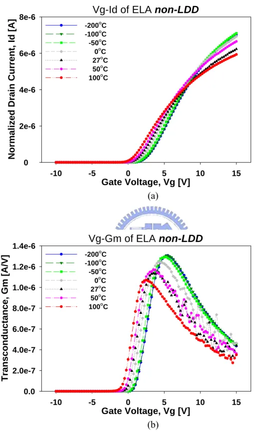
From the basic transfer characteristics curve of the non-LDD TFTs, the ID-VG
relations and transconductance, gm, of poly-Si TFT at the temperatures from -200°C to 100°C is shown in Figure 3-1-1. In Fig. 3-1-1(b), the maximum value of gm is
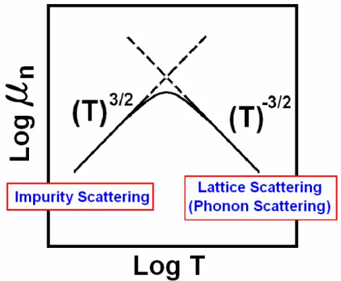
raised with the decreasing in temperature. This phenomenon can be explained by the evolutions of the carrier scattering in poly-Si TFT at high temperatures. Some reports have shown that the carriers in the MOSFET made on mono-crystalline silicon wafer suffer two types of scatterings, including impurity scattering and the phonon scattering, as shown in Figure 3-1-2 [3.1]. The phonon scattering is due to the lattice vibrations and strongly dependent on the temperature. The carrier transport of poly-Si TFT is evidenced to be mainly limited by the grain boundaries in the poly-Si film [3.2]. However, the field effective mobility of carriers should be affected by the phonon scattering within the same boundaries in channel region. At high temperature, the carrier is seriously scattered by the numerous phonon. Accordingly, the effective mobility of carrier is lower at high temperature than that at low temperature. Unlike the MOSFET, the poly-TFT owns lots of grain boundaries in the channel region. Thus, both the grain boundaries and phonons would deeply affect the carrier transport in the poly-Si TFT. Moreover, we focus on the conducting current in Figure 3-1-3.
Fig. 3-1-3 shows the ID-VG relations in linear scale of ID. We find a very
interesting phenomenon in the non-LDD TFTs, which is not observed in LDD TFTs. When the gate voltage is equal to the Vgti, the drain current is temperature
independent, so we named it the “cross point.” The Vgti is about 8.5V observed from
the figure. It indicates that for Vg<Vgti the Id current increases with T due to
positive temperature dependence of the diffusion process, whereas for Vg>Vgti the
current Id decreases with T due to the negative temperature dependence of the carrier
mobility, shown in Figure 3-1-1(b). That is, diffusion of carriers dominates the Id
current at the left of Vgti, and drift of carriers dominates the Id current to the right of
Vgti. At Vg = Vgti the transport mechanisms cancel each other, resulting in a bias
temperature is decreased to that of cryogenic temperatures, the Id current increases
for Vg>Vgti and decreases for Vg<Vgti. Thus, in the diffusion regime the leakage
current due to thermal processes diminishes, enhancing the signal-to-noise (S/N) behavior of the thin film transistor at cryogenic temperatures. [3.3]
The use of discontinuous models is widely accepted in the integrated circuit (IC) design field, so as to the thin film transistors design, similarly; that is, a different mathematical function is used for all three operating regimes of the TFT, and in most cases these functions have discontinuities at the border bias conditions in which the transistors switches from the subthreshold to linear regime and from linear to saturation regime. In the case of the subthreshold-to-linear transition, it is a generalized practice to say that the Id current for Vg>Vth is completely due to drift
and due to diffusion for Vg<Vth. This is the basic approximation used to derive
simple electrical models for the TFT. However, it is readily observed from Fig.
3-1-3 that the diffusion process is still acting for Vg>Vgti. In such a case at Vg = Vgti,
in the linear regime of operation, 50% of the current is due to diffusion and 50% is due to drift.
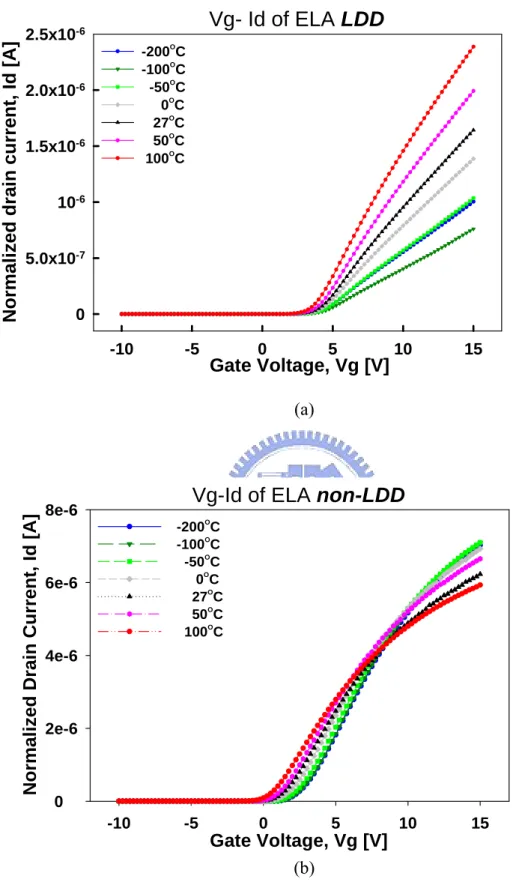
Figure 3-1-4 and Figure 3-1-5 shows the transfer characteristics VG-ID and
VG-Gm in the linear regime of the LDD and non-LDD devices manufactured by
ELA method, respectively. With temperature lowering from 100°C to -200°C, the sub-threshold slope shifted significantly and sub-threshold swing was better. The maximum value of Gm also shifted to right. Furthermore, we observed that the threshold voltage (VT) enhances and the off current rises with the increasing
temperature.
However, we noted a distinct phenomenon between the LDD and non-LDD devices. In the LDD devices, the mobility and on current decreased significantly with lowering of temperature while the non-LDD device showed little alteration
under temperature variations. The VT shift variation of the LDD device was larger
than the non-LDD device. The dominant mechanism in conducting capability of LDD TFTs should be different from the non-LDD TFTs. To clarify the difference between two structure devices, the sheet resistances of phosphorous heavily-doped and lightly-doped poly-Si film are measured in the previous work [3.4] shown in
Figure 3-1-6.
It’s apparent that the resistivity of heavily-doped film almost keeps well as the temperature changed. However, the LDD layer behaves as a temperature-dependent resistor which is a lager resistance at low temperature than at high temperature. The sheet resistivity of LDD at 50K is 4.72 times that at 300K. Since the LDD poly-Si sheet does not achieve the degeneracy doping level, the freeze effect of doped impurity atoms was observed. In addition, the traps of grain boundary play an important role for the conductivity of the poly-Si film. According to the Seto’s model, the electrons activated from the doped atoms, Phosphorous, were filled at the trap states at the grain boundaries. For simplify, the amount of free carrier in LDD layers, Nfree, can be equated to:
T D free N N
N = +−
(3-1) where ND+ is the number of ionized impurities and NT is the effective trap density.
Thus, the conductivity of poly-Si film is proportional to the amount of free carriers. With the decreasing of the temperature, the amounts of activated electrons are decreasing and the ratio of trapped electrons is rising by assuming that the amount of trap states is non-varied. The few free electrons are contributed to the conduction, and thus the conductivity is decayed at low temperature, shown in Figure 3-1-7. In heavily-doped poly-Si sheet, the amount of doped atoms is much larger than the trap density. Thus, the amount of activated electrons is much larger than the trap density
in heavily-doped poly-Si sheet since the high doping level would lead to the degeneracy. Seto has shown that the resistivity of boron doped poly-Si film as a function of the doping level. At high doping level (ND>>NT), resistivity of poly-Si
tends to approach the mono-crystalline one while the poly-Si may be degeneracy. Thus, heavily-doped poly-Si sheet exhibits the temperature-independent conducting behavior.
Figure 3-1-8 schemes that the LDD layers extended out the gate overlap region
behave as the temperature-dependent resistors and series connecting with the gate control region. Although the conductivity of channel region is reversion to the temperature, the LDD sheets extended outside the gate electrode behave as the large resistors and limit the drain current. When the temperature cooling the series resistance at the overlap between the source and drain, called the RS and RD, will
enlarge and lead the devices need the larger threshold voltage to turn on the TFTs. Thus, we can derive the decreasing current at low temperature from the conducting current formula: I Cox W
(
VGS VT)
DS L μ ⎛ ⎞ = ⎜ ⎟ − ⎝ ⎠ V (3-2) On account of the high resistivity caused by the lightly doped drain engineering, which has greater weight than the phonon scattering, that’s the reason why the “cross point” phenomenon only exhibited only in non-LDD TFTs.3.1.2 The Grain Boundary Effects
As mentioned at the beginning, the experiment is composed of four kinds of sample, the ELA, VGB, NGB and PGB TFTs. The distinction of those is the grain boundary orientation and existence. The orientation of the grain boundary in ELA TFTs is messy and irregularly, and in LGC (Lateral-Growth Crystallized) TFTs is
more regular and ordered. Furthermore, the LGC TFTs is divided into three parts: the grain boundary is vertical to the channel (VGB), and parallel with the channel (PGB), and no grain boundary exist in the channel regime (NGB).
Figure 3-1-9 and Figure 3-1-10 show the delta threshold voltage (ΔVth) and
delta field effect mobility (ΔμFE) as a function of temperature of the TFTs. In Fig. 3-1-9, the threshold voltage having the similar trend decrease with the elevating
temperature in LDD and non-LDD TFTs. In Fig. 3-1-10, we noted that the mobility increases with rising temperature in LDD TFTs while decreases in non-LDD TFTs. All of them have the similar trend and no distinct difference. Therefore, we concluded that the grain boundary orientation and existence in the channel region would not be the main factor to affect the characteristics of the TFTs. The main factor to affect the characteristics of the TFT is the LDD effect due to the series resistance, not concerned in the laser re-crystallized technology, regardless the Excimer Laser Annealing or the Lateral-Growth Crystallization process.
3.2 Negative Bias Temperature Instability in LTPS TFTs
We choose the P-type thin film transistors fabricated by the Excimer Laser
Annealing process in this experiment. In this research of negative bias temperature instability, abbreviated NBTI, we study the three topics: the dynamic recovery, the basic characteristics concluding the different stress temperature, stress bias and stress time, and the dimensional effects, containing the length and width effects.
3.2.1 Dynamic Recovery in NBTI
During the experiment, we find that the negative bias temperature instability seem to have the recovery phenomenon. In order to prove the assumption, we practice the experiment is described below. Select the devices with the same
dimension, channel length is 6μm and channel width is 30μm, under the same NBTI condition– the stress temperature is 100°C, the stress voltage VG is -10V, and the
stress time is 1000sec. After the NBTI stress, the electrical characterization measurement range (i.e. the applied gate voltage) is separate into two kinds: the extensive range containing both off and on states, VG=10 ~ -15V, and the smaller
range mainly focusing on the subthreshold regime, VG=2 ~ -8V. From the
experiment results, we find that the wider range of the applied gate voltage (VG=10~
-15V) has smaller degradation ~ 3.1717% than that of the smaller applied gate voltage (VG=2 ~ -8V) ~ 7.1349%, and rearranged detail results listed in Table 1.
This result is attributed to the hole de-trapping due to a lower applied gate voltage. During an electrical characterization, the stress is stopped and a lower gate voltage is applied to measure for instance threshold voltage. The threshold voltage shift is measured while a hole de-trapping occurs. Consequently, the apparent ΔVT is
decreased as the lower gate voltage is applied. Therefore, we know that the selection of the applied gate voltage range is an important factor affecting the underestimation of the device degradation.
Continuously, we perform the same NBTI condition mentioned above but the stress interruption is different. The former has no interruption and stressing 1000sec directly; the latter has stress interruption, 10, 20, 50 100, 200, 500, and 1000sec, respectively. Both have the same result that the lower applied gate voltage has the smaller degradation degree in ΔVT, while the latter with the multi-step stress
interruption has the smaller degradation, detail results is listed in Table 1 and Table
2. The result also related to the threshold voltage shift is measured while a hole
de-trapping happens simultaneously.
Finally, we sustain the electrical characterization after the stress removed shown in Fig. 3-2-1. We observed that during the NBTI stress the ΔVth is increased
while after the stress is removed the Vth degradation is diminished. Hence, the
waiting time (tw) between the stress and the IDS-VGS characterization will affect the
experimental result due to undervalue the degradation degree.
From the previous discussions, recovery phenomenon is related to hole de-trapping due to a lower applied gate voltage exhibiting the largest recovery in device characteristics, to the waiting time (tw) between the stress and the IDS-VGS
characterization, and to the stress interruption. The threshold voltage shift is measured while a hole de-trapping occurs. As a consequence, the apparent ΔVT is
decreased when the recovery influence is increased accordingly to the waiting time. Hence, recovery phenomenon is very critical for NBTI characterization and using the actual methodology requires special care to avoid underestimation of the ΔVT
due to oxide charge de-trapping at smaller oxide field [3.5], [3.6].
In order to improve the characterization of NBTI gradation, the selection of the applied gate voltage and stress interruption is very significant, and the waiting time for measurement is a critical element.
3.2.2 Characteristics of Negative Bias Temperature Instability
In this experiment, the channel length and width of the p-channel devices used
were 5 and 20μm, respectively. During the NBTI stress, the glass substrate is heated to the stress temperature (25°C, 50°C, 100°C, 125°C) and the stress voltage is -15V, -20V, and -25V, individually, is applied to the gate electrode while the source and drain electrodes grounded. The NBTI stress was periodically stopped (10, 20, 50, 100, 200, 500, 1000sec) to measure the basic electrical characteristics and all the measurements were performed at the stress temperature. The NBTI stress setup is revealed in Fig. 3-2-2.
Fig. 3-2-3 show the (a) output characteristics and (b) transfer characteristics of
the TFTs, respectively, before and after 1000sec NBTI stress at temperature 125°C with the stress voltage is -25 V. We observed that after NBTI stress, the threshold voltage shifted to the negative direction and device degradation occurs, containing the subthreshold swing, field-effect mobility (i.e. transconductance), and the drain current. The degradation of the subthreshold swing and field-effect mobility is due to the interface trap-state generation and the drain current can be derived from the drain current formula simply
(
)
FE ox ON GS th DS C W I V V V L μ = − (3-3) From the two parameters, mobility and threshold voltage shift, we can clearly see that the drain current will decrease after NBTI stress. In a word, the degradation of the drain current is attributed to the threshold voltage and field-effect mobility degradation after NBTI stress.From Fig. 3-2-4, we found the dependence of the threshold voltage shift on the stress time, stress temperature, and the stress voltage, respectively. In Fig. 3-2-4(a), the ΔVT increases upon increasing the stress time and shows the power law
dependence. And the ΔVT slightly fluctuates as a function of the stress time that is
because the magnitude of the ΔVT under NBTI stress is very small. Therefore, the
NBTI degradation is enhanced with the higher voltage and longer stress time. In Fig.
3-2-4(b) and (c), it is observed that the NBTI degradation is activated at higher
stress temperature or stress voltage, indicating that the NBTI can be thermally and electrically enhanced. From the three correlation diagrams from our experiment results and previous reports [1.29], [3.7], we can write the relational formula below
( Ea kT/ ) C VG
n th
V t e− e
Δ ∝ (3-4) where the exponent factor n is around 0.376~0.454 related to the hydrogen species,
the activation energy (Ea) extracted from the Arrhenius plot of Fig. 3-2-4(b) is about
0.07eV, the parameter C is extracted from (c) is around 0.047 to 0.055, which is a process parameter and independent of the stress voltage. The activation energy transform to the relative temperature is about 540°C, which is the temperature enough to break the Si-H bonds and creates the dangling bonds [3.8]. From the viewpoint, we can confirm that the fracture of Si-H bonds is actually a main element to lead the NBTI degradation.
Different from the MOSFETs, the TFTs own the numerous grain boundaries in the channel regions. Hence, we believe that besides the fixed oxide charges in the oxide layer and the trap-state creation in the Si/SiO2 interface, the trap-state creation
in the grain boundary also offer the ingredient to the threshold voltage shift possibly. As a result, we investigate the effects of grain boundaries in the LTPS TFTs during NBTI stress. Estimate the grain boundary trap densities utilized the Levinson and Proano method [1.13], [3.9] mentioned in Sec. 2.4 and Fig. 3-2-5. In Fig. 3-2-5, it is apparent that the grain boundary trap-state density increases after 1000sec NBTI stress from Eq. (2-9) and means that the grain boundary trap-state generation play an important role in the NBTI degradation for LTPS TFTs.
Fig. 3-2-6 shows the dependence of the grain boundary trap-state generation
(ΔNtrap) on the stress time, stress temperature, and stress voltage under various stress
conditions, respectively. The grain boundary trap-state density variation, like the threshold voltage shift, follows a power law dependence on the stress time with an exponent of 0.368 to 0.448, which is similar to the exponent factors extracted from
Fig. 3-2-4(a). Similarly, the relation between the grain boundary trap-state
generation and the stress temperature or the stress voltage has the same behavior with the threshold voltage shift discussed above in Fig. 3-2-4. In consequence, we found the ΔNtrap has the same function form as the threshold voltage shift, and it can
be represented as ( '/ ) ' ' E kTa C VG n trap N t e− e Δ ∝ (3-5) The parameters n’ is around 0.368 to 0.448, Ea’ is ranged from 0.06~0.08eV, and the
C’ value is 0.038~0.065, individually.
Compare the parameters extracted from the threshold voltage shift (n, Ea, and C)
and the grain boundary trap-state generation (n’, Ea’, and C’) in Fig. 3-2-7.
Apparently, it is worth noting that the value of the n’, Ea’, and C’ are similar to the n,
Ea, and C, respectively. It implies that the grain boundary trap-state generation and
the threshold voltage shift have the same dependence on the stress time, stress temperature and stress voltage. Subsequently, we picture the grain boundary trap-state generation and the threshold voltage shift relative diagram in Fig. 3-2-8. We noted that as the grain boundary trap-state density increases, the threshold voltage shift becomes larger and the two quantities are closely related for they have the same dependence on the stress time, stress temperature, and stress voltage. For this reason, we have verified that the grain boundary trap-state generation is closely related to the NBTI degradation mechanism in low temperature poly-silicon TFTs.
Besides the grain boundary trap-state generation as discussed above, the interface trap-state at the poly-Si/SiO2 interface also created in the LTPS TFTs
during NBTI stress. Fig. 3-2-9 reveals that the correlation between the subthreshold swing degradation and the threshold voltage shift of the LTPS TFTs after NBTI stress. The subthreshold swing has been reported to be closely related to the trap states located near the midgap (deep states), which originate from dangling bonds
[3.10]. So we conjecture that the NBTI stress leads the broken at the poly-Si/SiO2
interface and then generates more dangling bonds, resulting in the increase of interface trap states. As a result of the measurement scope of applied gate voltage is
focused on the psudo-subthreshold regime, by neglecting the depletion capacitance in the active layer and assuming no grain boundary trap-state existence, the effective interface-trap-state density (Nit) near the poly-Si/SiO2 interface can be simplified
derived from the subthreshold swing (S.S.) [3.11] 1 ln10 ox it C S q N kT q ⎛ ⎡⎛ ⎞⎛ ⎞ =⎢⎝⎜ ⎟⎜ ⎟− ⎜ ⎠⎝ ⎠ ⎣ ⎦ ⎝ ⎠ ⎞ ⎤ ⎟ ⎥ (3-6) From Eq. (3-6), we can say that the interface trap density at the poly-Si/SiO2 is
proportional to the subthreshold swing. Therefore, Fig. 3-2-9 can express that the trap-state generation happens at the poly-Si/SiO2 interface. In conclusion, the
trap-state creation occurs both in the grain boundaries and at the poly-Si/SiO2
interface under NBTI stress for LTPS TFTs.
The NBTI degradation in MOSFETs is pervasive assigned to the generation of fixed oxide charges and the interface trap states. Nevertheless, in our experiment for the LTPS TFTs the results indicate that the grain boundary trap-state generation must be considered to refine the degradation mechanism. The results showed that both the threshold-voltage shift (ΔVth) and the grain boundary trap-state generation
(ΔNtrap) have almost the same power law dependence on the stress time. The
exponent value n is about 0.36 to 0.45, which is explained by the diffusion-controlled electrochemical reactions [3.12], [3.13]. By spreading the model proposed for bulk-Si MOSFETs [3.13], we reproposed a model to explain the NBTI degradation mechanism for LTPS TFTs in Fig. 3-2-10. The NBTI degradation model can be described by the following:
( ) ( )
( ) ( )
Si H interface and grain boundary Si O Si gate oxide
Si interface and grain boundary Si fixed oxide charge+ Si OH e−
≡ − + ≡ − − →
≡ • + + ≡ − +
We suppose that the poly-Si/SiO2 interface and grain boundary are passivated by