行政院國家科學委員會專題研究計畫 成果報告
高品質定向奈米碳管場發射顯示器模組之實現研究-設計、
分析與模組化(III)
研究成果報告(精簡版)
計 畫 類 別 : 個別型 計 畫 編 號 : NSC 99-2221-E-151-015- 執 行 期 間 : 99 年 08 月 01 日至 100 年 07 月 31 日 執 行 單 位 : 國立高雄應用科技大學機械工程系 計 畫 主 持 人 : 鄭宗杰 共 同 主 持 人 : 謝健 計畫參與人員: 碩士班研究生-兼任助理人員:陳韋廷 碩士班研究生-兼任助理人員:朱世華 報 告 附 件 : 出席國際會議研究心得報告及發表論文 處 理 方 式 : 本計畫可公開查詢中 華 民 國 100 年 10 月 26 日
行政院國家科學委員會補助專題研究計畫
■成果報告
□期中進度報告
高品質定向奈米碳管場發射顯示器模組之實現研究-設計、
分析與模組化(3/3)
計畫類別:■個別型計畫 □整合型計畫
計畫編號:NSC 99-2221-E-151-015-
執行期間: 99 年 8 月 1 日至 100 年 7 月 31 日
執行機構及系所:國立高雄應用科技大學機械工程系
計畫主持人:鄭宗杰
共同主持人:謝健
計畫參與人員:陳韋廷,朱世華
成果報告類型(依經費核定清單規定繳交):■精簡報告 □完整報告
本計畫除繳交成果報告外,另須繳交以下出國心得報告:
□赴國外出差或研習心得報告
□赴大陸地區出差或研習心得報告
■出席國際學術會議心得報告
□國際合作研究計畫國外研究報告
處理方式:
除列管計畫及下列情形者外,得立即公開查詢
□涉及專利或其他智慧財產權,□一年□二年後可公開查詢
中 華 民 國 100 年 10 月 18 日
附件一The study of high quality orientation carbon nanotube for field emission
display application(3/3)
Final Report (NSC 99-2221-E-151-015)
Principal investigator: Tsung-Chieh Cheng1 Cooperate investigator: Jiann Shieh2
Department of Mechanical Engineering, National Kaohsiung University of Applied Science, Kaohsiung, Taiwan Department of Materials and Chemical Engineering, National United University, Miaoli, Taiwan
E-mail: [email protected]
Abstract
The main objectives of these three-year projects is to realize a carbon nanotube field emission display module through the novel thin film growth instrument design for well-aligned and high-purity carbon nanotubes growth. Our goal accords with what the government promotes in a more cost-effective manner- “Two Trillion - Double Stars” Plan. In our first-year project last year, a large-scale and cost-effective production of high-quality carbon nanotubes was successfully grown on flexible carbon cloth substrate by our designed CVD chamber. These high quality carbon nanotubes were also achieved by using a mixing gas of alcohol and NH3 which can suppress the defects on the surface of carbon nanotubes. In order to improve the performance of field emission displays, it is important to grow the well aligned CNT and know the field emission properties of nanoemitters. In our second-year project this year, we also designed field emission measurement instrument for the investigation of the field emission (FE) properties of high-technology materials. Field emission measurements were obtained within high vacuum chamber (background pressure bellow 10-6 Torr) and the measurements were performed in the characterization system. In final year of our project, due to the complexity of field emission measurement, we also want to establish the standard field emission measurement process. Moreover, in recent years, as the devices march toward to nano size, the classical method is not enough to measure very small area because of quantum effect and screen effect. Therefore, in order to obtain the results precisely, this proposal will also develop the fabrication of nano or sub-nano tips by setting up the experimental instruments and processing procedures.
Advances in research into many vacuum microelectronics devices depend upon the realization of reliable high intensity electron sources. For this reason, the ability to fabricate uniform emitters is an important factor in many vacuum microelectronics applications, including their use as electron sources in various visualization equipment, electron beam lithography, electron microscopy, microwave power devices, and especially for the fabrication of next-generation flat panel displays[1]. Over the past decade, field-emission properties have been studied extensively for various materials and geometrical arrangements, in which performance has been found to strongly depend upon the inherence, morphology, material density, and the sharpness, aspect ratio and surface conditions of the tip, to name a few. Recently, the advent of new nanofabrication techniques has led to the preparation of efficient electron emitters from various one-dimensional systems comprising different elements—including hollow nanotubes, solid nanowires, coaxial cable structures, side-by-side biaxial nanowires, and nanobelts—that can deliver highly bright electron beams from a narrow energy spread. Therefore, hoe to design the easy fabrication, low cost, and high performance field emitter, to understand quantitatively the physical picture of a single field emitter or field emitters array participating in the field-emission process are very important topics.
Experiment
In MWCNTs case, all samples were grown by CVD on the flexible carbon cloth substrate. A Fe film of 20 nm was used as a catalyst and patterned with a size of 0.5 × 0.5 cm2. The reactant gases were a mixture of H2 and CH4 with a ratio of 90:30 sccm at a pressure of 10 Torr. The microwave power of 300 W was applied to generate the plasma. After heating at 550 ◦C for 20 min, vertically aligned MWCNTs with similar height were uniformly grown over the carbon cloth. These as-grown MWCNTs then underwent a two-step chemical surface modification procedure. In step 1, MWCNTs were modified by 14 M HNO3 at 90 ◦C for 12 h for the carboxylation of MWCNTs, i.e. caps of closed MWCNTs were removed, forming an open-ended shape. In step 2, the thiolation ofMWCNTs was introduced by a method based on the pre-formation of carboxylic bonds of MWCNTs. After refluxing with deionized water to remove residual HNO3, thiolated MWCNTs were obtained by reacting with 2 M 2- mercaptoethanol (C2H6OS) in a dehydration reaction at 90 ◦C for 12 h. Besides, in nanowires case, a large area, uniform, and well-defined SiNWs on (110) Si wafers were fabricated by the direct high-density hydrogen plasma etching (DHDHPE) in NDL (National Nano-devices Laborities)
without any assistance from patterned mask or catalyst. During the hydrogen plasma etching, the silicon substrate was etched selectively by hydrogen ion flux and sputtered off, where the nanowires density was mainly controlled by the etching time.
Results and Discussion
In our studies, first, in order to understand the physical picture of field emission phenomena, the field-emission characteristics of a single silicon nano-emitter were investigated by means of experiments and simulation models. The emitters array was fabricated by dry etching using an inductively coupled plasma (ICP) through a three-step process[2]. A novel experimental measurement technique by SEM with nanomotors including the constant voltage and the constant emission modes was developed. In the constant voltage mode, we applied a larger voltage (e.g. 400 V) at the tungsten anode, which was greater than the expected turn-on voltage. Then, the tungsten probe was controlled by the nanomotor to move at a constant speed of 30 nm s− 1 through a longer distance than for the constant emission mode, and we concurrently measured the emission current to determine the approximate position where the maximum emission current occurs. In the constant emission mode, we moved the tungsten anode through a shorter distance around the approximate position of the maximum emission current determined in the constant voltage mode and measured the turn-on voltage at each position to find out where the minimum turn-on voltage occurs. By combining these two steps, we can precisely determine the ‘right’ position to measure the emission current from a single nano-emitter. Note that this novel technique can be adapted easily to measure the emission current from other types of nanoscale emitters. Accompanying these measurements, a parallelized 3D PIC code using the finite-element method coupled with a ray-tracing module was also developed and applied to simulate the field-emission process of single emitter[3]. Figure 1(a) illustrates the steady-state potential distribution along with a snapshot of the emitted electrons. At steady state, there were approximately 3000 electrons in the computational domain. Most of the electrons were emitted from the tip region having very high electric field (up to∼50 Vnm− 1). Figure 1(b) shows the comparison between the experimental and simulated I–V curves. In figure 1(b), the simulated emission currents for the case where the space–charge effect was taken into account compared very well with those observed experimentally; conversely, those generated without considering the space–charge effect generally appear much larger than those from the
experiments. A reduced emission current, relative to the case that did not account for the space–charge effect, results from the emitted electron clouds near the cathode (tip) surface. This reduction in the emission current reduces the local electric field at the tip surface or equivalently the shielding effect due to the charge particles. Therefore, our experimental and simulation data both clearly demonstrate that the space–charge effect due to the emitted electrons is important in determining the field-emission current from a nano-emitter in the present configuration. Our simulation and experimental results for the turn-on voltage show less than a 9.3% difference. The results also reveal that the field emission from a single silicon tip is a typical barrier-tunnelling, quantum mechanical process.
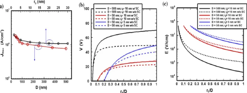
Besides, the theoretically simulation of the effect of space charge on FE nanodevices displaying different geometries, dimensions and work functions of their emitter materials, including diode and triode structures are also investigated as shown in Fig. 2[4]. To study the space-charge-limited FE of an FE nanodiode featuring a nanogap, in this study we derived an analytical model starting from Poisson’s equation. We prepared FE nanodiodes featuring a variety of gap distances and work functions of the cathode. For the integrally gated FE nanotriodes, we proposed a more realistic modified ball-in-sphere model[5] to study the effects of space charge on FE nanotriodes; this model considers the geometry effect and the actual work function of the nanoemitter. By solving the coupled FN equation and Poisson’s equation numerically for spherical coordinates, we investigated the influence of space charge on the emission current density of the FE nanotriodes. Specifically, we defined a threshold current density of space-charge limitation to characterize the anti-space-charge abilities of FE nanotriodes. Figure 3(a) reveals that the value of Jthsc decreased upon
increasing the dimensions of both the gate aperture and the emitter radius. To verify this behavior, we further examine the potential and electric field distributions (figures 3(b) and (c), respectively) for the FE nanotriodes (1)–(3) under a constant emission current density of 4 × 10⁶ A cm−2. In figure 3(b), when the space charge is taken into consideration, the required gate voltages for the FE nanotriodes (1)–(3) were 42, 22 and 20% greater than those required in the space-charge-free cases, respectively. Because of the presence of space charge, the value of EPoisson was lower than that of ELaplace at the same emission current density. In figure 3(c),
the electric fields for the FE nanotriode having values of D and r0 of 50 and 5 nm, respectively, were the
strongest, whereas those for the FE nanotriode having values of D and r0 of 500 and 10 nm, respectively, were
field amplification effect. Obviously, a higher electric field would negate the formation of space charge, thereby lessening its effect and increasing the threshold current density. Therefore, scaling the emitter radius and gate aperture of FE nanotriodes to smaller dimensions will lower the operating voltage and overcome the space-charge effects.
Moreover, the well aligned MWCNTs[6] which were grown by MPCVD was also compared with the random MWCNTs which were grown by thermal CVD on the flexible carbon cloth substrate to discuss the structure effect of the CNTs’ field emission properties. Figure 4(a),(b) shows the SEM images of these two MWCNT samples by MPCVD and thermal CVD. The results indicated that the MWCNTs grown by MPCVD (MP-CNTs) are well aligned and more uniform than MWCNTs grown by thermal CVD (T-CNTs). Obviously, due to more aligned and uniform CNTs will produce the uniform emission currents through the uniform electric field, in our field emission experiments, the field emission propertie of MP-CNTs is better than T-CNTs. Besides, in our works, we report a study on two-step surface chemical modifications on MWCNTs with the aim of improving the field emission properties of the MWCNTs. In step 1, MWCNTs were modified by 14 M HNO3 at 90 ◦C for 12h for the carboxylation of MWCNTs[7], i.e. caps of closed MWCNTs were
removed, forming an open-ended shape. In step 2, the thiolation of MWCNTs was introduced by a method based on the pre-formation of carboxylic bonds of MWCNTs. In this study, the thiolated MP-CNTs depict the lowest turn-on field of 0.2 Vμm− 1 and threshold field of 1.25 Vμm− 1, which are defined as the value of macroscopic fields producing the emission current density of 10 μAcm−2 and 1 mAcm−2, respectively.
According to our previous studies, we found that how to grow the well aligned field emitters is an important key factor for field emission devices but it is hard to form the well aligned uniform field emitters through the “growth” method. For this reason, we demonstrate a new one-step approach to the maskless fabrication of silicon nanowires through hydrogen plasma etching in the absence of a catalyst as shown in Fig.4(c)[8]. The results indicate that during hydrogen plasma etching the silicon substrate was sputtered off and the density of nanowires decreased with increasing the etching time, as a result of some nanowires bundling together, while their lengths increased. Our results indicate that the field emission properties are improved upon increasing the etching time; this process sharpens the nanowires’ geometry and lowers their work function. We hope that these highly uniform with respect to length, diameter, and distribution nanowires display great potential for application within many field emission nanoelectronics devices.
References:
1. J. M. Bonard, H. Kind, T. Stockli and L. O. Nilsson, Solid-State Electron. 45 (2001) 893.
2. T. C. Cheng, K. H. Hsu, P. Y. Chen, W. J. Huang, J. S. Wu, H. T. Hsueh and M. N. Chang, Nanotechnology 18 (2007) 225503.
3. J. S. Wu and K. C. Tseng, Int. J. Numer. Methods Eng. 63 (2005) 37.
4. P. Y. Chen, T. C. Cheng, J. H. Tsai and Y. L. Shao, Nanotechnology 20 (2009) 405202. 5. M. Ding, G.Sha and A. I. Akinwande, IEEE Trans. Electron.Devices 49 (2002) 2333.
6. F. T. Chuang, P. Y. Chen, T. C. Cheng, C. H. Chien and B. J. Li, Nanotechnology 18 (2007) 395702. 7. N. Rajalakshmi, H. Ryu, M. M. Shaijumon and S. Ramaprabhu J. Power Sources 140 (2005) 250.
8. T. C. Cheng, J. Shieh, W. J. Huang, M. C. Yang, M. H. Cheng, H. M. Lin, and M. N. Chang, Appl. Phys. Lett. 88 (2006) 263118.
Figure 1. (a) Potential distribution along with snapshot of electrons in the exploded view near the nano-emitter tip and (b) Comparison of the experimental and simulated current–voltage curves (work function = 4.5 eV).
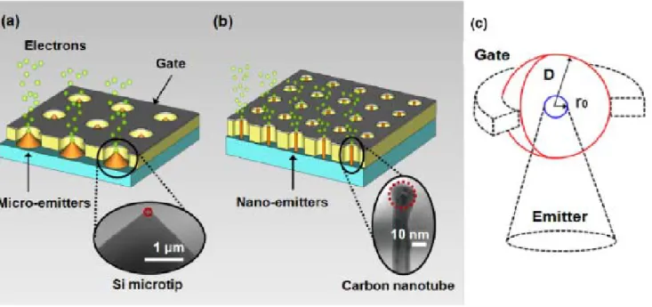
Figure 2. Schematic representations of (a) FE microtriodes possessing microtips as emitters, (b) FE nanotriodes possessing low-dimensional nanomaterials as emitters and (c) the ball-in-sphere model.
Figure 3. (a) Threshold current densities of space-charge limitation plotted with respect to the dimensions of the gate aperture (○) and emitter radius (○). (b) Potentials and (c) electric fields for FE nanotriodes possessing various device dimensions. The solid and dashed lines represent results obtained with and without the consideration of space-charge effects.
Figure 4. The SEM images of MWCNTs were grown by (a) MPCVD and by (b) thermal CVD and (c)the SEM images of well aligned silicon nanowires were etched by hydrogen plasma.
[Note] Self Evaluation
From NSC founding for these three-year projects, we developed two instruments, published 6 SCI papers and 10 conference papers (3 times are invited talks) as following:
(1) Journals:
1. F. T. Chuang, P. Y. Chen, T. C. Cheng, B. J. Lee, “Synthesis and field emission properties of thiolated carbon nanotubes on a flexible carbon cloth substrate”, Nanotechnology 18, 395702 (2007). (SCI: 3.310)
2. P. Y. Chen, T. C. Cheng*, J. H. Tsai, and Y. L. Shao, “Space charge effects in field emission nanodevices”, Nanotechnology 20, 40, 405202(2009). (SCI:3.446)
3. T. C. Cheng, C. H. Cheng*, Z. Z. Huang, and G. C. Liao,” Development of an energy-saving module via combination of solar cells and thermoelectric coolers for green building applications”, Energy 36 133-140 (2011). (SCI:2.952)
4. P. Y. Chen*, T. C. Cheng*, J. Shieh, and Y. C. Luo, “Nanomanipulation of field emission measurement for vacuum nanodiodes based on uniform silicon nanowire emitters”, Applied Physics Letters 98 163106 (2011). (SCI:3.554)
5. T. C. Cheng*, W. S. Lin, and S. Y. Wu, “Improved Field Emission Properties of Opened Carboxylated Multiwall Carbon Nanotubes on Flexible Carbon Cloth Substrate” have been accepted by Advance Science Letters. (SCI:1.253)
6. T. C. Cheng, T. H. Chen*, T. H. Fang, and T. U. Ye, “The Temperature Effect of Carbon Nanotubes Grown on Flexible Substrate by Atmospheric Thermal CVD” have been accepted by Advance Science Letters. (SCI:1.253)
7. 鄭宗杰、林毅、紹雲龍、楊忠諺,"奈米場發射元件之空間電荷效應研究", 奈米通訊, 17 卷, 第 一期 p.47 (2010).
(2) Conference papers:
1. P. Y. Chen, T. C. Cheng*, F. T. Chuang, J. S. Wu, H. L. Chen, B. J. Lee and E. Jones, ”The influence of geometry effect for field emission properties of Multiwall Carbon Nanotubes”, AM-FPD conferences,Japan,P-7 (2007).
2. T. C. Cheng*, L. Tsai, Y.H. Mao, C. W. Hsu, P.Y. Cheng, C.C. Cheng, Nanomanipulation Measurement and Parallel Pic Simulation of Field-Emission Properties from a Single Crystallized Silicon Emitter” ICN+T conference, ICN+T conference, 114, (2008).
3. T. C. Cheng*, “The Growth of MWCNTs on a Flexible Carbon Cloth Substrate by Thermal CVD and Microwave Plasma CVD”, IEEE-NanoMed conference, invited speaker (2008).
4. T. C. Cheng*, L. Tsai, S. Y. Wu, P. Y. Chen, C. C. Cheng and C. W. Hsu, “The Field Emission Properties and Growth Mechanisms of Multi-Wall Carbon Nanotubes on a Flexible Carbon Cloth Substrate” , ICNM conference, invited speaker (2009).
5. T. C. Cheng*,” The Field Emitters' design and fabrication of field emission devices”, The International Conference on Recent Trends in Materials Science and Technology(ICMST), invited speaker (2010). 6. C. W. Hsu, P. Y. Chen, T. C. Cheng, W. J. Huang, M. H. Cheng, and J. Hsieh, “Investigation of Field
Emission Characteristics of Silicon Nanowires by Nano-manipulation Probe in Scanning Electron Microscopy “, Symposium on Nano device Technology(SNDT), Hsin-Chu, Taiwan, T3-08, 2007. 7. C. C. Cheng, P. Y. Chen, T. C. Cheng, F. T. Chuang, and C. W. Hsu, “The Influence of Geometry
Effect for Field Emission Properties of Multiwall Carbon Nanotubes “, Symposium on Nano device Technology(SNDT), Hsin-Chu, Taiwan, T3-09, 2007.
8. T. U. Yeh, C. W. Hsu, S. Y. Wu, Y. L. Shao, and T. C. Cheng*, “The Temperature Effect of Carbon Nanotubes Grown on Flexible Substrate by Atmospheric Thermal CVD", 奈米工程暨微系統技術 研討會(NMTC), Hsinchu, Taiwan, 03-1226, July 9-10 (2009).
9. C. L. Hung, S. Y. Wu, C. C. Cheng, C. W. Hsu, Y. L. Shao, J. S. Wu, and T. C. Cheng*, " Effect of Interlayer for Carbon Nanotubes Grow on Carbon Cloth by Thermal Chemical Vapor Deposition", 奈米元件技術研討會論文集(SNDT), Hsinchu, Taiwan, NF-14, April 29-30 (2009).
10. 林毅、吳聲堯、陳韋廷、蘇恭賢、朱世華、鄭宗杰*” 以碳布基材在不同種子層上成長奈米碳管 及場發射特性之研究" 中國機械工程學會第 27 屆全國學術研討會論文集, 台北 D20-007, 10-21 Dec. (2010).
(3) Instruments:
2. Field emission measurement equipment: 項目 規格 溫度 23~900oC 壓力 760 torr ~ 5*10-3torr 氣體 NH4 0~100 sccm N2 0~400 sccm Ar 0~400 sccm C2H5OH 0~200 sccm 電漿 DC 300KW
國科會補助專題研究計畫項下出席國際學術會議心得報告
日期: 年 月 日計畫編
號
NSC 99-2221- E -151 -015-
計畫名
稱
高品質定向奈米碳管場發射顯示器模組之實現研究-設計、分析
與模組化(III)
出國人
員姓名
鄭宗杰
服務機
構及職
稱
國立高雄應用科技大學機械工
程系 助理教授
會議時
間
100 年 7 月 3 日
至
100 年 7 月 7 日
會議地
點
法國,史特拉斯堡
會議名
稱
(中文)
(英文)19th International Symposium on the Photophysics
and Photochemistry of Coordination Compounds
發表論
文題目
(中文)
(英文)
The Design of a Low Consuming Power Solar Heat
Collection Tracker for Stirling Engine Applications
19th International Symposium on the Photophysics and Photochemistry of
Coordination Compounds 報告
服務機關: 國立高雄應用科技大學機械工程系 出國人: 鄭宗杰 職稱: 助理教授 出國地點: 法國、史特拉斯堡 出國時間: 7/3~ 7/7, 2011 一、目的:參加 19th International Symposium on the Photophysics and Photochemistry of Coordination Compounds 以了解全世界在最先進發光奈米材料技術的發展趨勢,作為本實 驗室在半導體最新之製程技術用於下世代顯示元件開發的參考與借鏡。
19th International Symposium on the Photophysics and Photochemistry of Coordination Compounds 是結合歐洲表面科學、化學合成科技與材料研究,並由多家廠商 贊助的大型國際會議。其中聚焦最多的光電奈米材料合成與檢測方面的研究與開發則與本 實驗室的發展方向相當接近,所以藉著此次參加會議的心得,希望能夠為本實驗室未來的 研究方向提供最先進的指標。本次會議內容集中在發光奈米材料(nano materials)與光學檢 測(nano characterization)相關的研究,包括在製程整合的研究亦有相當不錯的論文發表,相 當值得我們學習,與會心得則略述於後。
19th International Symposium on the Photophysics and Photochemistry of Coordination Compounds 在法國、史特拉斯堡舉行。全世界各大廠商、大學、研究機構從事與光學功能 性材料技術相關之研究人員踴躍出席,今年與會的人數約超過五百人。會議的重點集中在
材料化學合成或物理成長方面的技術及其在發光元件之應用。此外,如光電檢測、奈米化 學、奈米光學、奈米醫學光學檢測等方面亦多有所著墨。
二、過程
參加有關 19th International Symposium on the Photophysics and Photochemistry of Coordination Compounds 之國際會議,可增加對最先進光電功能性材料技術之新知,瞭解 其發展趨勢,提升自己及實驗室研究水準。更可藉機與相關研究人員直接討論研究心得。
由於奈米技術的發展非常迅速,包括光電功能性材料合成與製程技術。此外,由於奈 米技術所牽涉到的材料與製程方式相當具有多樣性,因此新的微小化製程技術在奈米製程 中也扮演著非常重要的角色。在國際上幾個相當知名的研討會議,都是世界各地業界及學 術 界 所 積 極 參 與 的 , 而 此 19th International Symposium on the Photophysics and Photochemistry of Coordination Compounds 會議亦是其中在光電功能性材料製備與應用方 面較具代表性的會議之一。因此為獲得較先進的光電功能性材料技術發展資訊,參加該會 議是非常必要的;第一天議程的內容集中在功能性材料相關技術,製程則是以奈米粒子合 成為主,另外壁報論文也是會議這幾天的重點。以下則將會議內容作一重點的整理與敘述。
會議內容之重點之一是以光電奈米材料製備為主,利用該技術或結合光譜技術即可產 生出一些令人耳目一新的應用;當天就不同的議題而有數場邀請演講,報告中將節錄兩場 邀請演講於後:
1、 由美國 Northwestern University 的 J.-P. Sauvage 教授被大會邀請主講的 Multicomponent transition metal complexes: From charge separation to light driven molecular machines。其 演講內容說明如何利用光激發來組成相關功能性分子,包含如何合成相關材料與轉化 分子結構並得到相關光學性能等等,相關照片如下圖所示。
2、 由日本東京大學的 S. Kitagawa 教授主講的 Soft Porous Coordination Polymers Having Optical Properties。他是利用壓印技術與相關化學合成技術製作出相關光電功能性材 料,並利用控制孔洞大小與不同聚合物成分控制出具有固定波段的光電材料,以作為 來相關顯示用途。
演講大部份都是來自學術界,包括許多歐美日的學校等,此外,演講還包括各家光 電以及檢測儀器大廠,如 Veeco 與 Park 等。 第一天會議後則開始有壁報的解說;參展壁報解說則是在下午舉行,壁報展大部份 都是由各研究機構所貢獻,內容則依領域不同而分開舉行,相關會議演講過程如下圖所 示,在此不一一贅述。
三、心得 參加這次會議的主要目的是想瞭解目前世界上光電檢測、光電顯示器方面的研究, 因此,舉凡與該技術有關的演講與壁報解說都盡可能參加。藉由聆聽別人的演講內容, 獲 得 了 一 些 在 光 電 材 料 製 備 與 相 關 製 程 上 的 新 穎 想 法 。 包 括 以 膠 體 微 影 (Colloid lithography)技術製作光電奈米功能性材料、利用相關光激發表面電漿共振應用於生醫 領域尤其令人印象深刻。此外,改變奈米結構的尺寸與形狀造成吸收峰位置的偏移,亦 啟發了新的應用思考。其中壁報展覽時比較吸引我的是外籍研究人員利用橢偏儀作為表 面電漿共振檢測設備以及各種利用光電檢測偵測生物薄膜的技術,其原理與方法已用數 位相機拍攝,期能作為本實驗室相關研究的參考。 四、建議事項 在這次會議當中經由聆聽演講、閱讀研究成果壁報,以及與國外專家的交流中,瞭 解目前微影以及奈米製作技術的最新進展,獲益良多,也獲得許多新的想法,對本計畫 有相當大的助益。此外與會的學術機構所發表的論文的特色是作者利用各種零組件搭配 實驗室常見的儀器,即可產生新的功能與應用,如此的想法有助於本人研究發展的方向。 並期望在未來應加強不同研究領域的交流,如此才能激盪出創新的研究課題。
參 加 19th International Symposium on the Photophysics and Photochemistry of Coordination Compounds,收穫良多,心得如上所述。希望有機會能再次參加如此重要之國 際會議。最後附上這次研討會論文摘要一份。
五、附錄
The Design of a Low Consuming Power Solar Heat Collection Tracker for
Stirling Engine Applications
T. C. Cheng*, T. D. Fang, D. C. Chen, C. C. Wang and I. Lin
Department of Mechanical Engineering, National Kaohsiung University of Applied Science, Kaohsiung, Taiwan
E-mail: [email protected]
In recent years, with the fast development of science and technology, the demand for the energy is more and more imperative. Finding energy sources to satisfy the world’s growing demand is one of society’s foremost challenges for the next half-century.[1] Solar stirling electrical generator is a device that can convert sunlight heat energy into mechanical motion to form the electrical power. For stirling generator, in order to receive heat energy from the sunlight, the solar tracker, a device that keeps photo-thermal devices in an optimum position perpendicular to the solar radiation during daylight hours is necessary to increase the collected energy. Therefore, in this paper, an experimental study was performed to investigate the effect of using a passive continuous operation two-axes tracking on the solar heat energy collected.
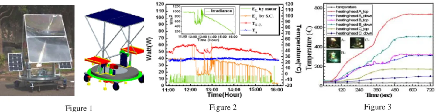
The proposed passive-operated two-axes heat collection solar tracker system which was developed as shown in Fig.1 consists of the following parts: (1) controlled circuit and programming, (2) the electro-mechanical mechanism, (3) Fresnel lens module. (4) heating head and data recorder. In our system, 8051 microprocessor was used to control two tracking motors in order to minimize the consumed energy of solar tracker system. Fresnel lens which relies the construction of lenses of large aperture and short focal length can easily concentrate light on to a fixed receiver or any heating head of any external combustion engine to generate power such as the stirling engine. Two-axes tracking method (azimuth/elevation tracking) which was calculated by Walraven[1] was used in our controlled program to determine the position of the sun and two solar cells were installed on both side of solar tracker to provide the all power of tracking system. Fig.2 showed the energy gain of solar cells(Eg), energy loss of motor(EL), solar irradiance,
temperature of solar cells(Tsc) and ambient temperature(Ta) at 4 min intervals for one partially
day in summer. The results indicated that the collected energy of solar cells is greater than the consumed energy of motors if there is no cloud to cover the sun. According to our experiment, the total collected energy by solar cells is about 533.41kJ and the total energy loss of all tracking system is about 80.3kJ. Besides, for stirling engine applications, the temperature of the heating head is an important factor to reveal the power that the engine is received. Fig.3 presented different solar heating focal areas and positions on heating head will strongly influence the temperature of heating head. The results indicated that if we can decrease the heat loss area (the area that sunshine didn’t shine or add the insulated material), the temperature of heating head of engine will increase faster and higher and the stirling engine will get more power.
1. H. Mousazadeh et al., Renewable and Sustainable Energy Reviews 13 (2009) 1800–1818. 2. R. Walraven, Solar Energy 20 (1977) 393–397.
國科會補助計畫衍生研發成果推廣資料表
日期:2011/10/19國科會補助計畫
計畫名稱: 高品質定向奈米碳管場發射顯示器模組之實現研究-設計、分析與模組化 (III) 計畫主持人: 鄭宗杰 計畫編號: 99-2221-E-151-015- 學門領域: 其他–機械工程技術無研發成果推廣資料
99 年度專題研究計畫研究成果彙整表
計畫主持人:鄭宗杰 計畫編號: 99-2221-E-151-015-計畫名稱:高品質定向奈米碳管場發射顯示器模組之實現研究-設計、分析與模組化(III) 量化 成果項目 實際已達 成數(被接 受或已發 表) 預期總達成 數(含實際 已達成數) 本計畫 實際貢 獻百分 比 單位 備註(質 化 說 明 : 如 數 個 計 畫 共 同 成 果、成 果 列 為 該 期 刊 之 封 面 故 事 ...等) 期刊論文 0 0 100% 研 究 報 告 / 技 術 報 告 2 2 100% 國內 論文著作 研討會論文 4 2 200% 篇 1.J. Y. Yang, T. C. Cheng, C. W. Hsu*, J. S. Wu and Y. L. Shao, ’A Study of Annealing Temperature Effect for ZnO Thin Film Grown on Glass Substrate Using Reactive Magnetron Sputtering’, Symposium on Nano device Technology (SNDT), Hsin-Chu, Taiwan, NF-32, May 4-5, (2010). 2.鄭金祥、王麒嘉、林毅、 朱胤福、施順榮、張克勤、 蘇恭賢、鄭宗杰*, ’雙軸 聚光型太陽追蹤系統應用 於史特靈引擎加熱端之聚 焦集熱研究’, 中華民國 力學學會第三十四屆全國 力 學 會 議 , 雲 林 , I2028, 19-20 Nov. (2010).以碳布基材在不同種子層 上成長奈米碳管及場發射 特性之研究’ 中國機械工 程學會第 27 屆全國學術研 討 會 論 文 集 , 台 北 D20-007, 10-21 Dec. (2010). 專書 0 0 100% 申請中件數 0 0 100% 專利 已獲得件數 0 0 100% 件 件數 0 0 100% 件 技術移轉 權利金 0 0 100% 千元 碩士生 2 2 100% 博士生 0 0 100% 博士後研究員 0 0 100% 參與計畫人力 (本國籍) 專任助理 0 0 100% 人次 國外 論文著作 期刊論文 4 2 100% 篇 1.C. W. Hsu, T. C. Cheng, C. H. Yang, Y. L. Shen, J. S. Wu, ’Effects of oxygen addition on physical properties of ZnO thin film grown by radio frequency reactive magnetron sputtering’ Journal of Alloys and Compounds 509 1774–1776 (2011). (SCI:2.135) 2.T. C. Cheng, C. H. Cheng*, Z. Z. Huang, and G. C. Liao,’ Development of an energy-saving module via combination of solar cells and thermoelectric
of gold nanoparticles’, Optic Express, 19 4768-4776 (2011). (SCI:3.278)
4. P. Y. Chen*, T. C. Cheng*, J. Shieh, and Y. C.
Luo, ’Nanomanipulation of field emission measurement for vacuum nanodiodes based on uniform silicon nanowire emitters’, Applied Physics Letters 98 163106 (2011). (SCI:3.554) 研 究 報 告 / 技 術 報 告 0 0 100% 研討會論文 2 1 100% 1.T. C. Cheng*,’ The Field Emitters' design and fabrication of field emission devices’, The International Conference on Recent Trends in Materials Science and Technology(ICMST), invited speaker (2010). 1.J. Y. Yang, M. H. Lin, S. T. Choi, W. C. Jhong, T. C. Cheng, L. Tsai and W. H. Lin, ’The Characteristics and Growth Mechanism of Bi2Te3 Thin Film grown on ITO Glass Substrate’ 3rd International Congress on Ceramics (ICC3), Osaka, Japan, Nov. 14-18 (2010). 專書 0 0 100% 章/本 申請中件數 0 0 100% 專利 已獲得件數 0 0 100% 件 件數 0 0 100% 件 技術移轉 權利金 0 0 100% 千元
碩士生 0 0 100% 博士生 0 0 100% 博士後研究員 0 0 100% 參與計畫人力 (外國籍) 專任助理 0 0 100% 人次 其他成果
(
無法以量化表達之 成果如辦理學術活 動、獲得獎項、重要 國際合作、研究成果 國際影響力及其他 協助產業技術發展 之 具 體 效 益 事 項 等,請以文字敘述填 列。)1. P. Y. Chen*, T. C. Cheng*, J. Shieh, and Y. C. Luo, ’Nanomanipulation of field emission measurement for vacuum nanodiodes based on uniform silicon nanowire emitters’, Applied Physics Letters 98 163106 (2011). 本 篇 論 文 被 獲 選 刊 登 於 Virtual Journal of Nanoscale Science & ; Technology 2. 共同指導學生參加茂迪杯獲得設計組第三名 成果項目 量化 名稱或內容性質簡述 測驗工具(含質性與量性) 0 課程/模組 0 電腦及網路系統或工具 0 教材 0 舉辦之活動/競賽 0 研討會/工作坊 0 電子報、網站 0 科 教 處 計 畫 加 填 項 目 計畫成果推廣之參與(閱聽)人數 0
國科會補助專題研究計畫成果報告自評表
請就研究內容與原計畫相符程度、達成預期目標情況、研究成果之學術或應用價
值(簡要敘述成果所代表之意義、價值、影響或進一步發展之可能性)
、是否適
合在學術期刊發表或申請專利、主要發現或其他有關價值等,作一綜合評估。
1. 請就研究內容與原計畫相符程度、達成預期目標情況作一綜合評估
■達成目標
□未達成目標(請說明,以 100 字為限)
□實驗失敗
□因故實驗中斷
□其他原因
說明:
2. 研究成果在學術期刊發表或申請專利等情形:
論文:■已發表 □未發表之文稿 □撰寫中 □無
專利:□已獲得 ■申請中 □無
技轉:□已技轉 □洽談中 ■無
其他:(以 100 字為限)
相關發表論文如結案報告書所示3. 請依學術成就、技術創新、社會影響等方面,評估研究成果之學術或應用價
值(簡要敘述成果所代表之意義、價值、影響或進一步發展之可能性)(以
500 字為限)
1.本研究為三年計畫,藉由國科會之支持,目前已完成一碳管製作機台與場發射量測設備, 相關結果也被具有代表性的期刊所接受 2.本研究已經在可撓性基板碳布上發展出場發射源的製作,未來可應用於相關軟性可撓的 場發射發光元件3.本研究也對單根場發射源作一精準研究與分析,並針對相關 screen effect, space charge effect 等影響建立出相關之模型,並與實驗比對,其結果十分吻合
4.本研究建立一標準的場發射量測模型,可供相關場發射研發人員參考借鏡
5.本研究執行共訓練出 6 位研究生,畢業後也順利進入相關產業如:大立光,台積,友達,奇 美,科林研發等相關光電半導體產業