Numerical Simulation on Pulsed Operation of an
All-Semiconductor Optical Amplifier Nonlinear
Loop Device
Jyh-Yang Wang, Jiun-Haw Lee, Yean-Woei Kiang, Member, IEEE, and Chih-Chung Yang
Abstract—Pulsed-signal self- and cross-switching operations in an all-semiconductor-optical-amplifier (SOA) nonlinear optical loop device are numerically investigated. The device consists of a loop amplifier, a multimode-interference waveguide amplifier (MMIWA), an input leg, and an output leg. With the combined mechanisms, including nonlinear coupling in the MMIWA, lateral field redistribution and amplification by the loop, and asymmetric gain–phase modulation between two counterpropagating signals in the loop, the device operates with efficient power-dependent switching. Simulations were conducted using a modified time-do-main traveling-wave method for the interplay between the two counterpropagating signals in MMIWA and loop. Typical pa-rameter values of GaAs–AlGaAs multiple quantum-well (MQW) optical amplifiers were adopted for simulating separately pub-lished experimental conditions. Numerical results of simulation agreed well in physical trend with the reported experimental data. Index Terms—Nonlinear optical loop device, numerical simula-tion, optical switch, semiconductor optical amplifier (SOA).
I. INTRODUCTION
A
LL-OPTICAL nonlinear switching devices of the Sagnac interferometer type have received much attention due to their potential applications in high-speed communications and signal processing. Such a device basically consists of a loop structure for providing power-dependent gain–phase modula-tion and a 2 2 coupler for signal splitting–combination. When the input signal splits equally or unequally into two counter-propagating components in the loop, which contains a material of nonlinear optics effect, these two counterpropagating waves experience different gain–phase modulations. This difference then determines the distribution of signal power between the two output ports of the 2 2 coupler after the aforementioned two counterpropagating components recombine at the coupler. Because the cumulated difference in gain–phase modulation de-pends on the power level of input signal, the output power dis-tribution of the device can be controlled by the input power. Such input power dependent behaviors can be used for self- and cross-switching operations in several applications.Manuscript received April 30, 2001; revised August 3, 2001. This work was supported by National Science Council, R.O.C., under Grants NSC 89-2215-E-002-033, NSC 89-2218-E-002-097, NSC 89-2218-E-002-094, and NSC 89-2218-E-002-095.
The authors are with the Department of Electrical Engineering, Graduate Institute of Communication Engineering, and Graduate Institute of Electro-Op-tical Engineering, National Taiwan University, Taipei 106, Taiwan, R.O.C. (e-mail: [email protected]).
Publisher Item Identifier S 0733-8724(01)09640-2.
The idea of this type of devices was first proposed and im-plemented as a nonlinear optical loop mirror (NOLM) [1]–[3]. An NOLM is an all-fiber device, consisting of a fiber loop and a fiber coupler. Because the nonlinear mechanism in the fiber loop is the Kerr effect, which is rather weak, a loop of several hundred meters long is usually needed for cumulating sufficient phase modulation. To increase optical nonlinearity and reduce the loop length, an SOA was usually asymmetrically inserted into the fiber loop [4]. Because the nonlinear phase modula-tion induced by gain saturamodula-tion in an SOA is much stronger than that induced by the Kerr effect in fiber, the loop length can be shortened. Such a device has been proposed for terahertz op-tical demultiplexing [4], [5]. The devices based on fiber loop have been widely used for system implementation; however, they are usually bulky and have long latencies. Recently, we reported the fabrication and continuous-wave (CW) signal op-eration of an all-SOA nonlinear loop device, showing efficient power-dependent switching [6],[7]. This work showed the ad-vantages of compactness and low latency. The configuration of this device is similar to an NOLM, including an SOA loop and an MMIWA for closing the loop. In CW-signal operation, the MMIWA is used as a coupler, not only for power splitting, but also for nonlinear coupling. The SOA loop is used for power amplification, as well as for rearranging the lateral field dis-tribution of the MMIWA. The combination of these functions leads to efficient nonlinear switching [8]. For the more prac-tical case of pulsed-signal operation, more physical mechanisms are involved. From the experimental data, it was found that the asymmetric gain distribution along the loop structure plays an important role [9]. In other words, the observed power-depen-dent switching results from the combined effects of asymmetric gain–phase modulation in the loop and nonlinear coupling in the MMIWA.
In this study, pulsed-signal self- and cross-switching opera-tions in such an all-SOA nonlinear loop device are numerically simulated. Device performances under various parameter con-ditions are investigated with relevant physical mechanisms in-terpreted. The numerical study was meant to simulate the ex-perimental condition [9]. Nevertheless, the real device opera-tion process could be too complicated to be studied with a fea-sible numerical model. Certain simplifications of device opera-tion mechanism are inevitable. With all of these consideraopera-tions, the numerical results are quite consistent in physical trends with the experimental observation [9]. Such numerical results would be useful for further optimization of device design and fabrica-tion. This paper is organized as follows. We derive the
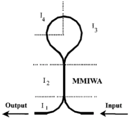
Fig. 1. Layout of the all-SOA nonlinear optical loop device.
ical formulations in Section II. A modified time-domain trav-eling-wave method for numerical computation is described in Section III. Discussed in Section IV are the simulation results. Finally, discussions and conclusions are given in Section V.
II. THEORETICALFORMULATIONS
Fig. 1 shows the layout of the all-SOA nonlinear optical loop device. The device consists of the loop, the MMIWA, the input port, and the output port. Note that the one-quarter and three-quarter sections of the loop are divided for different injection currents ( and , respectively). The injection currents for the regions of MMIWA and input–output portion are and , respectively. All parts are made of ridge-loading waveguide SOAs. The loop with a ridge width of 4 m (expected to form a single lateral-mode waveguide) is connected to the MMIWA with a ridge 8 m wide where two modes can propagate. Note that in practical situations, such as in our feasibility experiment, the fabricated MMIWA may accommodate more than two prop-agating modes. Therefore, the real device operation mechanisms may be more complicated than what is modeled here. Never-theless, the built model should be sufficient to describe the key mechanisms of the device operation. Also, the simulation results must be helpful to device design. The input and output ports also have a ridge width of 4 m. By injecting different currents, we can control the gain factors in different parts of the device. In nu-merical simulation, the effective index method is used to obtain the waveguide characteristics [10]. First, we analyze an effec-tive slab waveguide of thickness 0.43 m (along the transverse or direction) and find that only one guided mode exists in the epitaxial growth direction. Then, the lateral or -direction guid-ance is provided by an effective slab waveguide of a thickness equal to the ridge width. Here, the rectangular coordinates are adopted. Based on the device geometry, the signals propagate along the ridge-loading waveguides in both and direc-tions.
By inspecting the schematic diagram in Fig. 1, we can envi-sion how lightwaves propagate in the whole device. The input optical signal enters the device from the right leg and then dis-tributes its power over the lateral dimension upon entering the MMIWA. As propagating along the MMIWA, this lateral dis-tribution varies due to linear and nonlinear propagation effects. The wave field splits into two parts at the junction between the MMIWA and the loop. Then, the two counterpropagating waves
travel along the loop and recombine to form a new lateral dis-tribution at the junction to the MMIWA. The recombined wave propagates along the MMIWA in the backward direction until it arrives at the junctions to the input and output legs. Note that this backward-propagating wave may collide with the for-ward-propagating wave, resulting in the interplay of counter-propagation in the MMIWA. Finally, the wave splits between the input and output legs, depending on its lateral distribution at the junction of the MMIWA and input–output ports. Because the input and output legs are nothing but two uncoupled single lateral-mode waveguides and are used only for guiding signals besides possible amplification, we ignore them in our numerical simulations. In the remainder of this section, we briefly derive the equations for simulating the light wave propagation in the MMIWA and in the loop structure.
A. Counterpropagating Lightwaves in the MMIWA
In this study, we consider only the transverse electric (TE) polarized field. That is, the electric field is in the form
(1) Here, the dependence has been averaged out because the wave-field profile in the transverse direction is essentially un-changed during propagation under the single-mode assumption in that dimension. As mentioned previously, we assume that the MMIWA accommodates only two lateral modes, or its first two lateral modes play the major role. The electric field can, hence, be expanded into the combination of these two modes, each of which propagates in both and directions, as follows:
(2) Here, the extracted real function is the normalized lat-eral-mode distribution of waveguide mode 1 (2), satisfying the normalization condition
(3)
The four unknown complex amplitudes , ,
, and are slowly varying functions with
respect to and . is the optical angular frequency; is the propagation constant of the mode 1 (2) at angular frequency
. is the length of the MMIWA.
By substituting (2) into the wave equation, and after some mathematical manipulations, we can derive the coupled equa-tions governing the complex amplitudes [8]
(4b)
(4c)
(4d)
Here, we have defined and group velocity
, and introduced the material optical loss in the SOA as the internal loss constant . The gain func-tions are defined as the integrals of the gain constant , weighted with the modal field distributions, over the lateral di-mension as
(5) (6) The carrier-induced index change responsible for self-phase modulation (SPM) is accounted for with the linewidth en-hancement factor . From (4), it can be seen that there is direct coupling between two modes copropagating in either direction, but no such coupling exists between any two counterpropa-gating modes. This is so due to the fact that fast phase variation from the interference between two counterpropagating modes will be averaged out, producing no effective coupling. Nev-ertheless, two counterpropagating wave fields do affect each other indirectly through the gain functions influenced by the total light intensity [see (8) and (9)].
The electric field and the gain constant in the SOA are related through the rate equation for carrier density as
(7) where the four terms on the right-hand side (RHS) account for carrier injection, natural decay of carriers, carrier diffusion, and stimulated recombination, respectively. Here, is the injection current, is the elementary electric charge, is the active volume, is the carrier lifetime, is the diffusion coefficient, is the confinement factor in the -direction, and is the Planck’s constant divided by . For simplicity in notations, we define the electric field with a unit such that stands for the optical power density (W/m ).
Equation (7) is correct if the pulse duration is much longer than the intraband relaxation time, which takes place on a scale
of several hundred femtoseconds. Because the width and thick-ness of the SOA active region are much smaller while its length is much longer than the diffusion length, the carrier diffusion term in the rate equation can be neglected [11].
We assume that the gain constant is related to the carrier den-sity in a logarithmic manner through [12]
(8) where is a gain coefficient and is the transparency carrier density. By substituting (8) into (7) and neglecting the diffusion term, we obtain the rate equation for carrier density as
(9)
Now, the relevant equations have already been derived. Note that (4a)–(4d) is a set of nonlinear partial differential equations
for the complex field amplitudes with given gain
constant while is again related to the field
in-tensity through (8) and (9). Therefore, we can use (4), (8), and (9) to numerically solve the problem of counterpropagation of lightwaves in the MMIWA.
For cross-switching simulation, the theories above still hold except some modifications. In this situation, (4) should include eight differential equations, taking account of the counterprop-agating two modes for both pump and probe. Also, the RHS of (9) should include two stimulated recombination terms due to pump and probe. Although computation load is increased, there is no substantial difficulty in numerical simulation.
B. Counterpropagating Lightwaves in the Loop Structure
Because only one lateral mode propagates in the loop wave-guide, the wave field there can be expanded by the single-mode pattern with the slowly varying complex amplitude or for each direction of propagation. Here, we label the coordinate along the loop by as if it were a straight struc-ture. This is a reasonable approximation because the radius of the loop is much larger than wavelength. The possible bending loss due to loop curvature is taken into account by introducing a larger internal loss constant . Therefore, the governing equations for the counter-propagating complex amplitudes in the loop SOA are given by
(10a)
(10b) Here, the coupling term between two counterpropagating modes does not exist. However, the counterpropagating wave fields do affect each other through the gain functions which are controlled
by the total light intensity. Note that the aforementioned gov-erning equations for gain and carrier density are still valid for lightwave propagation in the loop structure.
III. NUMERICALALGORITHMS
To solve the problem of counterpropagation in a gain-satu-rated SOA (MMIWA or loop), the time-domain traveling-wave model [13] is adopted, with certain improvements. For illustra-tion, let us consider the situation in the MMIWA. We assume that the group velocities of two lateral modes are approximately
equal, i.e., . Using the moving temporal frames
and associated with the two
coun-terpropagating pulses, we can rewrite (4) as
(11a)
(11b)
(11c)
(11d) With local time coordinates and , the equations governing the wave fields become ordinary differential equations, facil-itating further mathematical manipulations. In simulation, the MMIWA is divided into small segments along the propagation axis with the step size about 5 m. We assume that two coun-terpropagating pulsed waves are incident upon the MMIWA from both ends. Each pulse consisting of two modes propagates in a gain-saturated SOA, governed by (9) and (11). As the two pulsed waves collide with each other, their fields add up to give the total field, which, in turn, changes the propagation environ-ment through (9). The changed gain function then affects the wave fields through (11), reflecting the nonlinear nature of our propagation problem. In other words, we solve the four
com-plex amplitudes , and over all the segments of
the MMIWA at each time instant. With the traveling-wave na-ture of (11), the wave fields at the next instant can be computed from the present wave fields and gain function. As time evolves, the spatial and temporal distributions of the counterpropagating optical fields can then be obtained step by step. To be specific, let us consider the propagation scenario in a segment
in detail. For incoming forward-propagating wave with
ini-tial complex amplitudes and , the
material-re-lated parameters and are assumed to
be constant in the segment . Then, (11a) and (11b)
are simultaneously solved to give the new complex amplitudes
and with .
Similarly, for an incoming backward-propagating wave with
ini-tial complex amplitudes and ,
the material-related parameters
and are assumed to be constant in the segment
. Then, (11c) and (11d) are simultaneously solved to
give the new complex amplitudes and
. This summarizes the evolution of the four complex ampli-tudes associated with the counterpropagating waves in the
seg-ment during time interval . Note that,
in our case, the differential equations (11a) and (11b) [or (11c) and (11d)] can be solved analytically in the segment
, and closed-form expressions are used. This makes our approach different from the usual time-domain traveling-wave model where the first-order finite-difference approximation to the partial derivative was used [13]. It is believed that our nu-merical results would be of better accuracy.
On the other hand, (9), for the carrier density, can be straight-forward solved at each spatial point to give the time evolution of the propagation environment, once the total field intensity at that point is given. In short, (9) and (11) interplay to determine the spatial and temporal distributions of the optical field.
The descriptions above are for the counterpropagation in the MMIWA. Similar algorithms are applicable to the case of the singe-mode loop structure, except that only two complex am-plitudes and satisfying (10) are to be solved.
IV. NUMERICALRESULTS
For simulating the pulsed operation of the device, the values of relevant parameters are listed in Table I. These values are chosen with reference to the experimental conditions [6]. Most of them are fixed in various simulation cases, unless specified otherwise.
A. Self-Switching Simulations
First, we consider the self-switching case. Fig. 2 shows the typical energy-dependent switching result, describing the output pulse energy versus the input pulse energy. The solid, dashed, and dash-dotted curves represent the output-pulse energies emerging from the output port, from the input port, and the sum of the two, respectively. Here, the small-signal gain
factor of MMIWA is 4 dB (corresponding to
the gain constant m ), and those ( and ) of the
three-quarter and one-quarter loop sections are 5 dB and 35 dB
(corresponding to m and 17 011 m ), respectively.
TABLE I
PARAMETERS FORNUMERICALSIMULATIONS
Fig. 2. Output-pulse energies (from the output port, input port, and their sum) versus input-pulse energy. The small-signal gain factorG of the MMIWA is 4 dB, and those (G and G ) of the three-quarter and one-quarter loop sections are 5 and 35 dB, respectively. The FWHM pulsewidth of the input pulse is 2 ps.
the input pulse is set at 2 ps. It is seen that, as the input-pulse energy increases from zero, the output-pulse energy increases, as well, at the beginning. However, nonlinear switching occurs when the input energy is high enough to induce significant gain saturation. Then, the curve for output energy declines. Also note that the total output energy becomes saturated as the input energy increases beyond a certain level. Here, the simulated results agree, in trend, with the reported experimental data (see [9, Figs. 6–8]).
In interpreting the CW-signal operation of the device, we at-tributed the nonlinear switching behaviors to the effect of non-linear coupling in the MMIWA and the functions of the lateral field redistribution and amplification from the loop [8]. Such considerations are still valid for pulsed-signal operation. How-ever, with pulsed signals, the loop asymmetry also plays an
Fig. 3. Output-pulse energy (from the output port) versus input-pulse energy for three values of MMIWA small-signal gain factorG . The small-signal gain factors(G ; G ) of the three-quarter and one-quarter loop sections are fixed at 5 dB and 35 dB. The FWHM pulsewidth of the input pulse is 2 ps.
important role. Nonlinear coupling in the MMIWA results in power-dependent lateral field distribution. After splitting into two counterpropagating components in the loop, they experi-ence different gain levels and phase shifts in the asymmetric loop. Such differences then combine with the nonlinear cou-pling effect induced during the backward propagation in the MMIWA to give power-dependent distribution of the signal en-ergy between the input and output ports.
We also investigate the effect of MMIWA gain factor on the performance of the device. Fig. 3 shows the output-pulse en-ergy (from the output port) versus the input pulse enen-ergy, with three values of MMIWA small-signal gain factor at 2 dB (dashed curve), 4 dB (solid curve), and 6 dB (dash-dotted curve). The small-signal gain factors of the three-quarter and one-quarter loop sections are fixed at 5 dB and 35 dB, respec-tively. Other parameters remain the same as in Fig. 2. When the
Fig. 4. Output-pulse energy (from the output port) versus input-pulse energy for three sets of small-signal gain factors(G ; G ) of the three-quarter and one-quarter loop sections. The small-signal gain factor of the MMIWA is fixed at 4 dB and the FWHM pulsewidth of the input pulse is 2 ps.
MMIWA gain factor becomes larger, the slope in the low-en-ergy region, where the operation is supposed to be linear, in-creases. This makes the nonlinear switching occur at a smaller input energy. From Fig. 3, one can also find that a larger value of leads to deeper and faster oscillation of the nonlinear switching curve. Hence, the value of is crucial for device op-eration of higher switching contrast and lower switching pulse energy.
To investigate the effect of loop asymmetry, we vary the small-signal gain ratio between the three-quarter and one-quarter sections of the loop with fixed total gain of the whole loop at 40 dB. Fig. 4 shows the results with different small-signal gain factors of the three-quarter and one-quarter
sections of the loop, with being 15 dB and 25dB
(dashed curve), 10 dB and 30 dB (dash-dotted curve), and 5 dB and 35 dB (solid curve). In all three cases, the small-signal gain factor of the MMIWA is fixed at 4 dB, and other parameters remain the same as in Fig. 2. It is found that the output-pulse energy decreases with increasing or decreasing . How-ever, the switching energy decreases with increasing gain ratio , implying that the increase of loop asymmetry leads to more efficient nonlinear switching.
The dependence of nonlinear switching on input-pulsewidth (FWHM) is illustrated in Fig. 5, with three values of at 1 ps, 2 ps, and 4 ps. For a given input pulse energy, a smaller corresponds to a higher peak intensity. The gain saturation, and, hence, the nonlinear switching, would occur at a smaller input energy. Nevertheless, the switching contrast, i.e., the ratio of output maximum over minimum, does not monotonically follow the pulsewidth variation.
We also vary the length of MMIWA to see its effect. As shown in Fig. 6, it is found that effective nonlinear switching oc-curs when the length of MMIWA is equal to one half of the cou-pling length of MMIWA. This value of MMIWA length is chosen in most of our simulations, as mentioned in Table I.
B. Cross-Switching Simulations
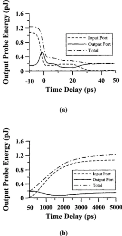
To investigate cross-switching phenomena, we conducted pump-probe simulation. Fig. 7 shows the output energies of the probe pulse (from the output port, from the input port, and the sum from both ports) as functions of the time delay between the pump and probe. Here, the positive (negative) time delay
Fig. 5. Output-pulse energy (from the output port) versus input-pulse energy for three values of FWHM pulsewidth of the input pulse. The small-signal gain factorsG ; G , and G are fixed at 4, 5, and 35 dB, respectively.
Fig. 6. Output-pulse energy (from the output port) versus input-pulse energy for three lengths of the MMIWA. The small-signal gain factorsG ; G and G are fixed at 4, 5, and 35 dB, respectively. The FWHM pulsewidth of the input pulse is 2 ps.
means that the pump leads (lags) the probe. For comparison, we also compute the light transit times in the different device segments. The transit times in the MMIWA and one-quarter loop are about 5.67 ps and 5.39 ps, respectively. The input energy of the pump pulse is 0.05 pJ and that of the probe pulse is 0.002 pJ. Both the pump and probe have pulsewidth at 2 ps. The small-signal gain factors and are fixed at 4 dB, 5 dB, and 35 dB, respectively. One can see that the curve of probe energy from the output port exhibits a hump around zero time delay and extends a long tail. This behavior can be interpreted qualitatively with the following mechanisms. When the probe leads significantly the pump, corresponding to a large negative time delay in Fig. 7(a), the probe is not affected by the pump. This situation corresponds to the linear optics case, and a small amount of energy comes out from the output port. As the probe leads the pump by a small time interval, such as several picoseconds, the counterclockwise-propagating probe pulse in the loop will experience gain saturation caused by the clockwise-propagating pump pulse in the region, including part of the high-gain one-quarter loop. Meanwhile, the clock-wise-propagating probe pulse in the loop will experience gain saturation caused by the counterclockwise-propagating pump pulse only in the low-gain loop region. The strong asymmetric gain–phase modulation experienced by the counterpropagating probe pulse then results in a significant variation of probe energy with respect to time delay. This explains the appearance
Fig. 7. Output energies of the probe pulse (from the output port, input port, and their sum) as functions of time delay between pump and probe. The input energy of the pump pulse is 0.05 pJ and that of the probe pulse is 0.002 pJ. Both the pump and probe are of pulsewidth 2 ps. The small-signal gain factors
G ; G and G are fixed at 4, 5, and 35 dB, respectively.
of the peak of probe energy from the output port. Note that in this situation, the clockwise-propagating (or the counter-clockwise-propagating) pump pulse produces no effect on the clockwise-propagating (or the counterclockwise-propagating) probe pulse because the pump lags behind the probe. When the pump leads the probe by a small time interval, corresponding to a small positive time delay in Fig. 7(a), the gain in SOA is saturated by the pump pulse. Therefore, less gain–phase modulation for the probe results in smaller variation of the probe energy. As the pump leads the probe further, the probe pulse experiences the gradually recovered environment. No significant asymmetric gain–phase modulation is now expected for the probe. Fig. 7(b) shows the output probe energies after time delay beyond 50 ps. It can be seen that the probe energy gradually attains its unsaturated level at the time delay of the order of nanoseconds. This is consistent with the fact that the carrier lifetime here is assumed to be 1 ns. Note, also, that our simulated results agree in trend with the reported experimental data (see [9, Fig. 15]).
Fig. 8 shows the dependence of cross-switching performance on the small-signal gain factor of MMIWA. It plots the output-probe energy (from the output port) versus time delay, with three values of at 2 dB (dash-dotted curve), 4 dB (solid curve), and 6 dB (dashed curve). Other parameters remain the same as in Fig. 7, except that the input-probe energy is reduced to 0.5 fJ. It is found that the larger is, the earlier the peak of output probe energy appears. This indicates that a higher probe-pulse energy (by stronger amplification) results in earlier switching in the pump–probe scheme.
Fig. 8. Output energy of the probe pulse (from the output port) versus time delay between pump and probe for three values of MMIWA small-signal gain factorG . The small-signal gain factors (G ; G ) of the three-quarter and one-quarter loop sections are fixed at 5 dB and 35 dB, respectively. The input energy of the pump pulse is 0.05 pJ, and that of the probe pulse is 0.5 fJ. Both the pump and probe are of pulsewidth 2 ps.
Fig. 9. Output energy of the probe pulse (from the output port) versus time delay between pump and probe for different lengths of the high-gain(G ) section of the loop with(G ; G ) fixed at 5 dB and 35 dB. Three lengths of the high-gain section are used: one-eighth (dashed curve); one-quarter (solid curve); and three-eighths (dash-dotted curve) of the whole loop. The small-signal gain factorG of the MMIWA is fixed at 4 dB. The input energy of the pump pulse is 0.05 pJ, and that of the probe pulse is 0.002 pJ. Both the pump and probe are of pulsewidth 1 ps.
To further understand the effect of asymmetric gain distribu-tion in the loop, we vary the length of the high-gain section with fixed at 5 dB and 35 dB. In Fig. 9, three lengths of the high-gain section are used: one-eighth (dashed curve); one-quarter (solid curve); and three-eighths (dash-dotted curve) of the whole loop. For meaningful comparison, one end of the high-gain section is fixed at the midpoint of the loop. Other parameters remain the same as in Fig. 7, except that the input FWHM pulsewidth is reduced to 1 ps. In Fig. 9, one can see that as the high-gain section becomes longer, cross switching occurs earlier. This trend can be explained with the aforemen-tioned physical mechanisms. As the probe pulse leads the pump pulse by a few picoseconds, the counterclockwise-propagating probe pulse in the loop will experience gain saturation caused by the clockwise-propagating pump pulse in the region involving the high-gain section. Also, the clockwise-propagating probe pulse in the loop will experience gain saturation caused by the counterclockwise-propagating pump pulse only in the low-gain loop section. The strong asymmetric gain–phase modulation ex-perienced by the counterpropagating probe signal results in a fast variation of the probe energy. Now, if the length of the
high-gain section increases, greater time delay between pump and probe pulses is allowed to evoke this phenomenon, and the curve of the output probe energy shifts toward the negative side of time delay accordingly. Therefore, Fig. 9 confirms that the asymmetric gain distribution along the loop is important for ef-ficient pulsed-signal operation.
V. DISCUSSION ANDCONCLUSION
Pulsed-signal operation of an all-SOA nonlinear optical loop device has been numerically simulated. In simulation, two-mode expansion was assumed for wave propagation in the MMIWA. Interplay between two counterpropagating waves in both the MMIWA and the loop was considered. The self- and cross-switching phenomena were induced by gain saturation and the associated phase modulation in semiconductor optical amplifiers. A modified time-domain traveling-wave method was used to simulate such a complicated pulsed-signal oper-ation scheme. Efficient power-dependent self-switching and cross-switching operations of the device have been demon-strated. The mechanisms behind the pulsed-signal operation of the device are different from those of CW operation. Besides the nonlinear coupling in the MMIWA and the lateral field re-distribution and amplification in the loop, the asymmetric gain distribution along the loop is crucial for efficient pulsed-signal operation.
Our proposed device has the advantages of compactness and short latency. From the simulations of self- and cross-switching operations, it is expected that high-speed operation of modu-lation or multiplexing–demultiplexing would be feasible. For example, a control (pump) pulse can be used to control the output level of the signal (probe) pulse, if the relative time delay is properly designed. However, the operation speed of the de-vice is ultimately limited by the gain recovery time, i.e., carrier lifetime. Other limitations include the bending loss in the loop structure and the amplified spontaneous emission (ASE) noise. The bending loss limits further size reduction of the device. The whole SOA design results in high ASE. The latter problem can be released by fabricating passive regions in the device using the quantum well intermixing technique.
The numerical study was meant to simulate the experimental condition [9]. Although the physical trends of the numerical re-sults are consistent with experimental data, differences can still be found. For instance, in Figs. 2 and 3, the oscillatory peak levels decrease with input power. However, experimental data showed increasing trends of such peaks (see [9, Figs. 6–8]). Also, in Fig. 7, after the peak near the zero delay, there is a long depression and then a tail at about the same level as the por-tion of negative time delay. Experiments showed slightly dif-ferent results, in which the depression duration is shorter and the tail level is relatively higher (see [9, Fig. 15]). Such differ-ences can be attributed to the more complicated mechanisms in real devices, compared with our simplified model. For ex-ample, the number of waveguide modes in the MMIWA can be more than two, leading to a more complicated counterpropa-gating scenario, which is beyond simulation capability. Also,
reflection can occur at several junctions of the device, particu-larly at both ends of the MMIWA and at the boundary between the high- and low-gain regions in the loop. Meanwhile, it is dif-ficult to determine the coupling length of the MMIWA. With all of these possible difficulties in simulating such a device, our numerical model did result in consistent physical trends. Our numerical simulations with various parameter values would be useful for optimization of device design and fabrication.
REFERENCES
[1] N. J. Doran and D. Wood, “Nonlinear-optical loop mirror,” Opt. Lett., vol. 13, pp. 56–58, 1988.
[2] K. J. Blow, N. J. Doran, and B. K. Nayar, “Experimental demonstration of optical soliton switching in an all-fiber nonlinear Sagnac interferom-eter,” Opt. Lett., vol. 14, pp. 754–756, 1989.
[3] M. E. Fermann, F. Haberl, H. Hofer, and H. Hochreiter, “Nonlinear am-plifying loop mirror,” Opt. Lett., vol. 15, pp. 752–754, 1990. [4] J. P. Sokoloff, P. R. Prucnal, I. Glesk, and M. Kane, “A terahertz
op-tical asymmetric demultiplexer,” IEEE Photon. Technol. Lett., vol. 5, pp. 787–790, July 1993.
[5] I. D. Phillips, A. Gloag, P. N. Kean, N. J. Doran, I. Bennion, and Ellis, “Simultaneous demultiplexing, data regeneration, and clock recovery with a single semiconductor optical amplifier-based nonlinear-optical loop mirror,” Opt. Lett., vol. 22, pp. 1326–1328, 1997.
[6] J. H. Lee, D. A. Wang, H. J. Chiang, D. W. Huang, S. Gurtler, C. C. Yang, Y. W. Kiang, B. C. Chen, M. C. Shih, and T. J. Chuang, “Nonlinear switching in an all-semiconductor-optical-amplifier loop device,” IEEE Photon. Technol. Lett., vol. 11, pp. 236–238, Feb. 1999.
[7] J. H. Lee, D. A. Wang, Y. W. Kiang, H. J. Chiang, and C. C. Yang, “Nonlinear switching behaviors in a compact all-semiconductor-optical-amplifier Sagnac interferometer device,” IEEE J. Quantum Electron., vol. 35, pp. 1469–1477, Oct. 1999.
[8] D. A. Wang, C. C. Chen, Y. W. Kiang, J. H. Lee, and C. C. Yang, “Nu-merical study on a compact all-semiconductor-optical-amplifier Sagnac interferometer device,” Opt. Quantum Electron., vol. 32, pp. 585–608, 2000.
[9] J. H. Lee, J. Y. Wang, C. C. Yang, and Y. W. Kiang, “All-optical switching behaviors in an all-semiconductor nonlinear loop device,” J. Opt. Soc. Amer. B., vol. 18, pp. 1334–1341, Sept. 2001.
[10] T. Tamir, Ed., Integrated Optics. New York: Springer-Verlag, 1977. [11] G. P. Agrawal and N. A. Olsson, “Self-phase modulation and spectral
broadening of optical pulses in semiconductor laser amplifiers,” IEEE J. Quantum Electron., vol. 25, pp. 2297–2306, Nov. 1989.
[12] L. A. Coldren and S. W. Corzine, Diode Lasers and Photonic Integrated Circuits. New York: Wiley, 1995.
[13] L. M. Zhang, S. F. Yu, M. C. Nowel, D. D. Marcenac, J. E. Carrol, and R. G. S. Plumb, “Dynamic analysis of radiation and side-mode suppression in a second-order DFB laser using time-domain large-signal traveling wave model,” IEEE J. Quantum Electron., vol. 30, pp. 1389–1395, June 1994.
Jyh-Yang Wang was born Taiwan, R. O. C., in 1976.
He received the B.E.E. degree from Chung Yuan Christian University, Chung-Li, Tyaoyun, Taiwan, in 1999 and the M.E.E. degree from National Taiwan University, Taipei, Taiwan, in 2000. He is currently pursuing the Ph.D. degree at the Graduate Institute of Communication Engineering, National Taiwan University.
His research interests are in computational electro-magnetics.
Jiun-Haw Lee, photograph and biography not available at the time of
Yean-Woei Kiang (S’81–M’84) was born in
Panchiao, Taiwan, R.O.C., in 1954. He received the B.S.E.E., M.S.E.E., and Ph.D. degrees from National Taiwan University, Taipei, Taiwan, R.O.C., in 1977, 1979, and 1984, respectively.
In 1979, he joined the faculty of the Department of Electrical Engineering, National Taiwan University, where he is currently a Professor. His research in-terests include wave propagation, scattering, inverse scattering, and optoelectronics.
Chih-Chung Yang received the B.S. degree from
National Taiwan University, Taipei, Taiwan, in 1976 and the M.S. and Ph.D. degrees from University of Illinois, Urbana-Champaign, IL, in 1981 and 1984, respectively, all in electrical engineering.
He joined the Department of Electrical and Com-puter Engineering, Pennsylvania State University, University Park, as an Assistant Professor in 1984. There, he received his tenure and was promoted to Associated Professor in 1990. He joined the Graduate Institute of Electro-Optical Engineering and Department of Electrical Engineering, National Taiwan University, in 1993 as a Professor. In August 2001, he became the Chairman of the Institute of Electro-Optical Engineering, National Taiwan University. His research interests include optoelectronics devices for optical fiber communications, nonlinear optics, semiconductor materials for UV blue-green light emission, biomedical photonics, and photonic crystals.