Fabrication of High Performance Low-Temperature Poly-Si
Thin-Film Transistors Using a Modulated Process
Ching-Lin Fanzand Mao-Chieh Chen
*
Department of Electronics Engineering and Institute of Electronics, National Chiao-Tung University, Hsinchu 300, Taiwan
A modulated process共MP兲 for the fabrication of low temperature processed 共LTP兲 polysilicon thin-film transistors 共poly-Si TFTs兲 using fewer processing steps but resulting in improved performance is investigated in this study. The modulated process is characterized by combining the solid-phase crystallization共SPC兲 step and the implant annealing into a single annealing step processed after the source/drain implantation. This is to say that the processing step of SPC is omitted, such that the SPC and implant annealing are conducted simultaneously. In this way, the process time is substantially shortened and the device perfor-mance is significantly improved. The improvement of device perforperfor-mance is presumably attributed to the larger poly-Si grain in the channel region processed by the MP scheme. In addition, the MP samples have a better NH3-plasma passivation efficiency than the conventional process共CP兲 samples; this also implies that the MP samples contain larger grains in the channel regions than the CP samples. The electrical stress-induced degradation of device characteristics for the NH3-plasma passivated MP samples is attributed to the carrier-induced metastable defects in the channel region.
© 2002 The Electrochemical Society. 关DOI: 10.1149/1.1452123兴 All rights reserved. Manuscript received August 26, 2001. Available electronically February 20, 2002.
Low temperature process共LTP兲 polysilicon thin-film transistors 共poly-Si TFTs兲 have been intensively studied for the application to large-area active matrix liquid-crystal display共AMLCD兲.1Their pri-mary advantages over the conventional amorphous silicon 共␣-Si兲 TFTs lie in their high driving current and the availability of both n-and p-channel TFTs. These features facilitate the integration of high performance complementary metal-oxide-semiconductor 共CMOS兲 peripheral drivers with active switching elements on a single glass substrate, thus reducing the number of external connections for im-proved reliability and reduced cost.2,3The channel films for these devices are typically deposited in an amorphous phase, which is then crystallized to become the large-grain polysilicon phase with a smooth surface. Solid-phase crystallization 共SPC兲 is a promising technique because of its simplicity, low cost, and excellent uniformity.4Given the upper limit of⬃600°C for processing on the glass substrates,5SPC using low-temperature 共600°C兲 furnace an-nealing requires very long anneal time共about 20 h or longer兲;6thus, it suffers from a substantial trade-off between performance and throughput. Various techniques have been employed to shorten the crystallization time, such as metal-induced crystallization,7plasma treatments before crystallization,8and laser-induced crystallization.9 However, these techniques require many extra processing steps or need expensive processing equipment. In addition, for the fabrica-tion of LTP poly-Si TFTs with tradifabrica-tional procedures, the implant annealing which is used to activate dopants and remove damage defects usually is carried out using furnace annealing at 600°C for a long time共about 12-24 h兲 after the source/drain implantation. The prolonged process time of both SPC and implant annealing causes low throughput in the fabrication of LTP poly-Si TFTs.
In this work, the LTP poly-Si TFTs were fabricated using a modulated process, in which the SPC and implant annealing are combined in one step so that the processing time is greatly reduced. This is to say that the processing step of SPC conventionally used for transforming the as-deposited amorphous silicon to polycrystal-line silicon is to be omitted, such that SPC and implant annealing are conducted simultaneously. Because the as-deposited amorphous silicon channel regions and the implanted source/drain regions are crystallized simultaneously, the grain size in the channel region will be enhanced due to the difference of crystallization velocity between the two regions. Thus, high performance LTP poly-Si TFTs can be fabricated using the modulated process共MP兲 with a higher through-put than the conventional process共CP兲. Furthermore, the passivation
scheme using NH3plasma is investigated with respect to the pro-motion of device performance. By comparing the difference of the passivation efficiency between the MP and the CP, we are able to identify the speculated mechanism that improves the TFT perfor-mance using the modulated process. Finally, the effects of dc elec-trical stress on TFT performance are also investigated.
Experimental
Two sets of self-aligned top-gated n-channel poly-Si TFTs were fabricated in this study using the CP as well as the MP. With regard to the devices fabricated by CP, the TFTs were fabricated following the traditional process procedures; this is, solid-phase crystallization 共SPC兲 was performed at 600°C for 24 h in N2ambient immediately after the deposition of amorphous silicon, and the implant annealing was performed also at 600°C for 24 h in N2 ambient after the source/drain implantation. As for the devices fabricated by MP, the process step of SPC was omitted and the implant annealing at 600°C for 24 h in N2 ambient was the only thermal process, which was performed after the source/drain implantation. Aside from being dif-ferent in this respect, all devices were fabricated according to the following procedures. A 110 nm thick low pressure chemical vapor deposition 共LPCVD兲 amorphous Si layer was first deposited on a 500 nm thermal-oxide-covered Si substrate at 550°C using a SiH4 process. Then, SPC was performed at 600°C for 24 h in N2ambient for phase transformation from amorphous silicon to polysilicon共for CP only, not for MP兲. Individual active regions were then patterned and defined. After a standard RCA clean, a 120 nm thick tetraethyl orthosilicate共TEOS兲 oxide was deposited to serve as the gate insu-lator. A second poly-Si film was subsequently deposited and pat-terned to define the gates of the devices. The TEOS oxide on the source/drain regions served as the etching stop because of the etch-ing rate difference between the TEOS oxide and poly-Si duretch-ing the reactive ion etching共RIE兲 gate etching. Next, the source/drain and gate regions were doped with phosphorus via self-aligned ion im-plantation at 40 keV to a dose of 5⫻ 1015cm⫺2. Then, implant annealing was performed at 600°C for 24 h in N2 ambient. A 500 nm thick PE-TEOS oxide was deposited at 300°C. Finally, contact holes were opened, and 500 nm thick Al electrodes were deposited and patterned, followed by a sintering process at 400°C for 30 min in N2ambient. To passivate the trap states in the poly-Si channel, a group of TFTs, including CP and MP fabricated devices, were sub-jected to NH3-plasma hydrogenation at 300°C for various times in a parallel plate reactor with a power density of 0.7 W/cm2. In this study, all devices investigated have a gate width/length of 24/4m.
*Electrochemical Society Active Member. zE-mail: [email protected]
Journal of The Electrochemical Society, 149共4兲 H93-H97 共2002兲
0013-4651/2002/149共4兲/H93/5/$7.00 © The Electrochemical Society, Inc.
The I-V characteristics of the fabricated devices were measured using an HP-4145B semiconductor parameter analyzer. Various de-vice parameters, including the threshold voltage (VTH), subthresh-old swing共SS兲, and minimum leakage current (IOFF) were measured at a drain voltage of VDS⫽ 5 V. The threshold voltage is defined as the gate voltage which yields a drain current (IDS) of 600 nA (IDS ⫽ 100 nA ⫻ W/L). The field-effect mobility (FE) is calculated from the maximum value of the transconductance at VDS⫽ 0.1 V. The maximum and minimum values of IDSat VDS⫽ 5 V are desig-nated as IONand IOFF, respectively.
Results and Discussion
Effects of modulated process on device characteristics.—Figure 1 shows the typical transfer characteristics (IDS-VGS) at VDS ⫽ 5 V for the poly-Si TFTs fabricated with two different processes, CP and MP. During the drain current measurement, the gate voltage was swept from⫺15 to 25 V. The measured as well as extracted key devices parameters, including VTH, SS, FE, IOFF, and ON/OFF current ratio (ION/IOFF) are summarized in Table I. Obvious im-provement in devices characteristics was obtained by using MP in-stead of CP, as shown in Table I, VTHdecreased from 13.8 to 11.3 V, SS decreased from 2.02 to 1.81 V/dec,FEincreased from 4.85 to
7.43 cm2/V• s, Ioffdecreased from 58.6 to 34.9 pA, and ION/IOFF ratio increased from 2.5⫻ 105 to 6.3⫻ 105. Figure 2 shows the typical output characteristics (IDS-VDS) at two different gate volt-ages for the poly-Si TFTs fabricated with two different processes, CP and MP. It can be seen that the TFTs fabricated with MP exhib-ited significant improvement in the turn-on state performance. This improvement in the performance of the MP fabricated devices is presumably due to the larger grain size in the poly-Si channel, in which the enhancement of grain size is believed to be arisen from the difference of crystallization velocity between the implanted source/drain and the deposited␣-Si channel regions.10
The crystallization from an amorphous phase to a polycrystalline phase occurs through two processes, nucleation and grain growth.11 As the SPC annealing proceeds, nuclei are first generated in the films, and the growth of nuclei into grain follows. The grain growth starts at nuclei formation and stops when the adjacent grains come into contact with each other. To obtain the largest grain size, low nucleation rate and high grain growth rate are indispensable.12 Moreover, it is well known that many implanted impurities, such as boron and phosphorus, have the effect of enhancing Si self-migration. Due to the increase in defect density in the implanted source/drain region, the self-migration coefficient is increased, caus-ing decreased activation energies for both nucleation and grain growth.13,14As a result, the nucleation rate and the growth rate of grain are increased in the implanted source/drain region. Thus, the crystallization time of the implanted source/drain amorphous re-gions will be significantly reduced.10
Based on the above discussions, a crystallization model is pro-posed to account for larger grain size in the channel regions of the MP samples. With the SPC process for the nondoping channel re-gions combined with the implant annealing for the doped source/ drain regions, nucleation sites will first appear in the implanted source/drain regions which have a higher nucleation rate due to larger self-migration coefficient. As the crystallization proceeds, nu-clei grow into grains and individual grains in the source/drain re-gions continue to grow and coalesce into larger grains, while the Figure 1. Transfer characteristics (IDS⫺ VGS) of poly-Si TFTs fabricated
with two different processes, CP and MP.
Table I. Comparison of device characteristics for poly-Si TFTs fabricated with the CP and the MP.
Parameters CP MP
Threshold voltage, VTH共V兲 13.8 11.3 Subthreshold swing, SS共V/dec兲 2.02 1.81 Field-effect mobility,FE共cm2/V s兲 4.85 7.43 Leakage current, IOFF共p/A兲 58.6 34.9 ON/OFF current ratio, ION/IOFF 2.5⫻ 10
5
6.3⫻ 105
Figure 2. Output characteristics (IDS⫺ VDS) of poly-Si TFTs fabricated with two different processes, CP and MP.
␣-Si in the nondoping channel regions remains in the amorphous state because the incubation time in this region is larger than that in the source/drain region. Subsequently, the coalescing grains can act as seeds to grow laterally into the␣-Si channel region. However, as the lateral growth proceeds and when the annealing time is larger than the incubation time of␣-Si channel regions, nucleation will also begin to occur in the channel region followed by the grain growth. Finally, the lateral growth will stop when the laterally grown grains come into contact with the self-formed grains of the channel regions. Thus, the channel regions are crystallized laterally from the nucleation sites formed in the source/drain areas but the nucleation and grain growth rates of the channel regions will limit the distance of lateral growth. Moreover, we believe that the larger the difference of crystallization rates between the doped source/ drain regions and the nondoping channel regions is, the larger the grain size will be in the channel regions. As for the CP, the grain size in the channel regions remains nearly unchanged during the implant annealing because the existing grains formed in the SPC step im-pede the regrowth of grains during the implant annealing.15Thus, we presume that the MP resulted in larger grains in the channel regions than the CP.
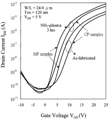
Effects of NH3-plasma treatment.—It has been reported that large grain poly-Si films have a better passivation efficiency as a result of low defect density because of their smaller grain boundary density.16Thus, to confirm the speculation that the MP fabricated devices contain larger grains in the channel regions共as described above兲, the completed poly-Si TFTs were subjected to NH3-plasma hydrogenation. Figure 3 shows the typical transfer characteristics (IDS⫺ VGS) of poly-Si TFTs before and after NH3-plasma treat-ment for 3 h. The plasma treattreat-ment clearly improved the transfer characteristic for both CP and MP devices. The measured, as well as extracted key devices parameters, are summarized in Table II. By comparing the date in Tables I and II, we found significant improve-ment in various devices characteristics for both CP and MP samples by the NH3-plasma treatment, in particular the MP samples. To dis-tinguish the passivation efficiency between the CP and MP samples,
the device characteristics were evaluated as a function of NH3-plasma treating time. Figures 4 and 5 show the percentage improvement共i.e., percentage decrease兲 in threshold voltage (VTH) and SS, respectively, as a function of NH3-plasma treatment time for both CP and MP samples. The extent of improvement in VTHand SS continuously increased with the passivation time, and the improve-ment rate of MP samples is higher than that of CP samples, in particular the improvement in SS as shown in Fig. 5. It is well known that the effective trap state density at the grain boundary of the poly-Si/SiO2interface and the poly-Si channel region is closely related to the subthreshold swing (S⫽ dVGS/d log IDS). By ne-glecting the depletion capacitance in the active layer, the trap state density NTcan be estimated from the relation17,18
NT⫽ COX q
冉
q KT S ln 10 ⫺ 1冊
where COXis the oxide capacitance. The trap state densities for the MP samples before and after the plasma passivation for 3 h are determined to be 5.28⫻ 1012and 3.32⫻ 1012cm⫺2, respectively, while the corresponding densities for the CP samples before and Figure 3. Transfer characteristics (IDS⫺ VGS) of poly-Si TFTs before and
after NH3-plasma treatment for 3 h.
Table II. Comparison of device characteristics for poly-Si TFTs fabricated with the CP and the MP after NH3-plasma treatment
for 3 h.
Parameters CP MP
Threshold voltage, VTH共V兲 9.5 6.9 Subthreshold swing, SS共V/dec兲 1.71 1.16 Field-effect mobility,FE共cm
2
/V s兲 11.7 17.3 Leakage current, IOFF共pA兲 51.2 27.7 ON/OFF current ratio, ION/IOFF 1.5⫻ 106 2.9⫻ 106
Figure 4. Improvement in threshold voltage共i.e., percentage decrease in
VTH兲 as a function of NH3-plasma passivation time for CP and MP samples. Journal of The Electrochemical Society, 149共4兲 H93-H97 共2002兲 H95
after the plasma treatment are found to be 5.91⫻ 1012 and 4.97 ⫻ 1012
cm⫺2, respectively. The NH3-plasma treatment significantly reduced the trap state density for both MP and CP samples, in par-ticular the MP sample. Since large grain poly-Si films have a better passivation efficiency because of their smaller density of grain boundary,16 the larger grain in the channel regions of the MP samples is presumably responsible for the larger extent of NT reduc-tion. Thus, the higher passivation rate and better characteristic im-provement for the MP devices, as shown in Fig. 4 and 5, imply that MP devices contain larger grain than the CP devices.
It has been reported that VTH and SS are closely related to the dangling bond midgap states, whileFEis dominated by the intra-granular band tail states in poly-Si TFTs. The dangling bonds mid-gap states have a faster response to hydrogenation, while the intra-granular tail states respond more slowly to hydrogenation. Only when the hydrogenation concentration is so large as to fill both the midgap states and the tail states will a significant fraction of the tail states be passivated. Moreover, if the interior of the grains contains a large number of tail states, the passivation will be slow for this type of defect.16 Thus, the NH3-plasma passivation resulted in a larger improvement in SS for the MP sample than for the CP sample, while the improvement inFEwas nearly the same for both MP and CP samples.
From the above discussions, we may conclude that, as a result of larger grain size and thus lower grain boundary density in the poly-Si channel, the MP sample has a better passivation efficiency on grain-boundary dangling bonds, leading to a better improvement in SS and VTH. The results are consistent with the speculation in the section on the Effects of the modulated process that the MP resulted in larger grain size in the channel regions than the CP. Thus, we suggest the combination of the SPC step and the implanting anneal-ing into a sanneal-ingle processanneal-ing step for the fabrication of LTP poly-Si TFTs with the conventional self-aligned scheme. In this way, the
devices characteristics can be improved while the process time is significantly reduced. Moreover, it is worth noticing that, if the dif-ference of crystallization rate between the doped source/drain re-gions and the nondoping channel rere-gions becomes sufficiently large, the modulated annealing process may result in only one single-grain boundary in the middle of the channel region for devices of very small dimensions. Thus, not only the device performance but also the characteristic uniformity can be improved, in particular the de-vices of very small geometry.
Reliability.—The reliability of poly-Si TFTs fabricated with the MP and NH3-plasma treated for 3 h, was investigated with respect to dc electrical stress. Figure 6 shows the changes in VTHas a function of stress time for ON-state stressing with VGS⫽ VDS⫽ 25 V. The percentage shift of threshold voltage ⌬VTH is defined ⌬VTH(%) ⫽ 关(VTH after stress ⫺ VTH before stress兲/VTH before stress兴 ⫻ 100%. It is found that the VTHincreased with the stress time, which is similar to the conventional LTP poly-Si TFTs reported in literature.19,20Furthermore, bothFEand IOFFremained nearly un-changed after the dc electrical stress. Since the measured IDS-VGS characteristics after the dc electrical stress are nearly equal for the forward and reverse modes, the charge trapping in the oxide is pre-sumably not the dominant degradation mechanism. Instead, the deg-radation of VTHis presumably due to the carrier-induced metastable defects within the channel regions. The formation of the carrier-induced metastable defects is attributed to the breaking of the weak Si-Si and Si-H bonds in the poly-Si channel regions by the channel carriers during stressing.20
Conclusions
The modulated process共MP兲 for the fabrication of LTP poly-Si TFTs was investigated. The MP is characterized by combining the solid-phase crystallization共SPC兲 with the implanting annealing into a single annealing step processed after the source/drain implanta-Figure 5. Improvement in subthreshold swing共i.e., percentage decrease in
SS兲 as a function of NH3-plasma passivation time for CP and MP samples.
Figure 6. Threshold voltage shift vs. stress time for poly-Si TFT fabricated with the MP and NH3-plasma treated for 3 h. The device was stressed at
tion. In this way, the process time is substantially shortened and the poly-Si grains in the channel region can be significantly enlarged. As a result of larger grain size, the performance of the poly-Si TFTs fabricated with the MP scheme is superior to those fabricated with CP. The formation of larger grain size by the MP scheme is attrib-uted to the difference of the crystallization velocity between the nondoping channel regions and the doped source/drain regions. Moreover, the passivation treatment by NH3-plasma improved the device characteristics, and the passivation rate for the MP samples is higher than that for CP samples, which may imply that the MP samples contain larger grains in the channel regions than the CP samples. The electrical stress-induced degradation of devices char-acteristics for the NH3-plasma passivated MP samples is attributed to the carrier-induced metastable defects in the channel region. In summary, the modulated process is a simple and high throughput process for the fabrication of high performance LTP poly-Si TFTs.
National Chiao-Tung University assisted in meeting the publication costs of this article.
References
1. T. Serikawa, S. Shirai, A. Okamoto, and S. Suyama, IEEE Trans. Electron Devices,
ED-36, 929共1989兲.
2. H. Oshima and S. Morozumi, Tech. Dig. - Int. Electron Devices Meet., 1989, 157.
3. S. D. Brotherton, Semicond. Sci. Technol., 7, 721共1995兲.
4. M. K. Hatalis and D. W. Greve, IEEE Electron Device Lett., EDL-8, 361共1987兲. 5. D. M. Moffatt, Mater. Res. Soc. Symp. Proc., 377, 871共1995兲.
6. M. K. Hatalis and D. W. Greve, J. Appl. Phys., 63, 2260共1988兲. 7. H. Kim, J. G. Couillard, and D. G. Ast, Appl. Phys. Lett., 38, 383共1995兲. 8. K. Pangal, J. C. Sturm, S. Wagner, and N. Yao, IEEE Trans. Electron Devices,
ED-47, 1599共2000兲.
9. T. Shameshima, S. Usui, and M. Sekiya, IEEE Electron Device Lett., EDL-7, 276
共1986兲.
10. N. Yamauchi and R. Reif, J. Appl. Phys., 75, 3235共1994兲.
11. K. Zellama, P. Germain, S. Squelard, J. C. Bourgoin, and P. A. Thomas, J. Appl.
Phys., 50, 6995共1979兲.
12. I. Suni, G. Goltz, M. G. Grimaldi, and M. A. Nicolet, Appl. Phys. Lett., 40, 269
共1982兲.
13. H. Yamamoto, H. Shiwara, and S. Furukawa, Appl. Phys. Lett., 46, 268共1985兲. 14. I. Mizushima, S. Kambayashi, T. Yoshida, M. Kinugawa, K. Ohori, H. Kuwano, S.
Onga, and J. Matsunaga, in Proceedings of 1990 International Conference on Solid
State Devices and Materials, p. 381共1990兲.
15. M. J. Tsai and H. C. Cheng, Thin Solid Films, 249, 244共1994兲.
16. I. W. Wu, T. Y. Huang, W. B. Jackson, A. G. Lewis, and A. Chiang, IEEE Electron
Device Lett., EDL-12, 181共1991兲.
17. T. Noguchi, H. Hayashi, and T. Ohshima, Jpn. J. Appl. Phys., 25, L121共1986兲. 18. C. A. Dimitriadis, P. A. Coxon, L. Dozsa, L. Papadimitriou, and N. Economou,
IEEE Trans. Electron Devices, ED-39, 598共1992兲.
19. C. F. Yeh, T. J. Chen, and J. N. Jeng, J. Electrochem. Soc., 144, 3645共1997兲. 20. I. W. Wu, W. B. Jackson, T. Y. Huang, A. G. Lewis, and A. Chiang, IEEE Electron
Device Lett., EDL-11, 167共1991兲.