Manuscript submitted November 27, 2006; revised manuscript received February 12, 2007. Available electronically May 4, 2007.
For anticipated applications of very large scale integration 共VLSI兲 technology, more advanced materials for gate dielectrics will be required. Although a physical gate thickness of ⬍1 nm for a complementary metal oxide semiconductor transistor with nitride/ oxynitride gate stacks has been demonstrated,1continued scaling for future semiconductor technology requires an equivalent oxide thick-ness of less than 1.0 nm for sub-65-nm metal oxide semiconductor field-effect transistor共MOSFET兲 devices.2 However, development of a dielectric thin film with an effective oxide thickness under 1.0 nm and an acceptable leakage current level will be very difficult, due to the high direct tunneling leakage current of nitride/oxynitride gate dielectrics. As a result, high-dielectric-constant共high-k兲 oxide thin films are currently attracting great interest as possible alterna-tives to nitrided-SiO2gate dielectrics.3-5
Various extrinsic gate dielectrics, including Ta2O5, Y2O3, ZrO2, CeO2, SrTiO3, BaSrTiO3共BST兲, and HfO2have been extensively investigated. Among these high-k gate materials, HfO2 gate dielectrics6-8are the most popular candidate currently under study, due to their high dielectric constant共25–30兲, wide energy bandgap 共⬃5.68 eV兲, and the high stability of their Si surface. At the mo-ment, capacitance-voltage 共C-V兲 hysteresis and charge trapping when the hafnium dioxide is applied to the MOSFET as the gate dielectrics,9-11 are critical problems for future ultralarge scale inte-gration共ULSI兲 technology applications of HfO2. Therefore, various methods have been used to ameliorate these problems, including cosputtering of silicon and aluminum with hafnium to deposit hafnium silicate and aluminate dielectrics,12,13 nitridation before HfO2deposition,14and oxidizing a sputtered metal nitride such as HfN15to form hafnium oxynitride共HfON兲 films.
Recently, fluorinated gate dielectrics have been shown to im-prove the SiO2/Si interface.16-19Furthermore, fluorine incorporation into the high-k gate dielectrics has been proposed, to improve both the thermal stability,20and the negative bias temperature instability 共NBTI兲 reliability.21,22
However, characterization of key aspects of fluorinated HfO2gate dielectrics formed by CF4plasma treatment, including the thermal stability of the gate leakage current and C-V characteristics, breakdown voltage, and effective oxide thickness, has not been well developed. In addition, neither charge trapping during electrical measurement nor the temperature dependence of the gate leakage current has been investigated.
In this paper, the characteristics of fluorinated HfO2gate dielec-trics using CF4 plasma treatment were demonstrated. Fluorinated HfO2 gate dielectrics show thinner effective oxide thickness
共⬃2.2 nm兲, smaller C-V hysteresis 共45 mV兲, low gate leakage cur-rent density 共⬃5 ⫻ 10−9A/cm2兲, high breakdown voltage 共⬃−9 V兲, better thermal stability, good distribution of electrical performance, and less charge trapping. A physical model is proposed to comprehensively explain the mechanism for electron and hole trapping in fluorinated HfO2thin film. Furthermore, the temperature dependence of the leakage current explains why the generated traps are effectively eliminated in fluorinated HfO2gate dielectrics.
Experimental
For the purposes of this research, MOS capacitors were fabri-cated. The silicon wafers used in this study were p-type 共100兲 Czochralski 共CZ兲 with a resistance of 4–7 ⍀ cm. Standard RCA cleaning was first performed on all samples. HfO2thin film was then deposited by reactive radio-frequency共rf兲 sputter method. Deposi-tion plasma was created by applying 150 W rf power to a 7.5 cm diam target positioned 15 cm away from the substrate. Hafnium dioxide deposition took place for 2.5 min, resulting in the formation of a 5 nm HfO2 thin film. After HfO2 thin film deposition, CF4 plasma was used to treat the HfO2thin film to form the fluorinated HfO2gate dielectrics. Some samples were treated under CF4plasma in the plasma-enhanced chemical vapor deposition共PECVD兲 sys-tem, whose chamber volume is 3.76⫻ 105cm3. The cathode diam-eter was 40 cm, and the distance between the cathode and the holder was 4 cm. The sample was loaded into the substrate at an elevated temperature共300°C兲. The reactive pressure and the flow rate of the CF4gas were 600 mTorr and 500 sccm, respectively. The rf power was 40 W with CF4plasma exposure times of 1 and 5 min共termed P-1 and P-5, respectively兲. For the normal HfO2 gate dielectrics samples共denoted as as-deposited兲, there was no CF4plasma treat-ment after the hafnium dioxide deposition. Postdeposition annealing 共PDA兲 was performed on rapid thermal anneal 共RTA兲 equipment at 700°C for 30 s in N2ambient. Samples with PDA treatment were called as-deposited/A, or P-1/A and P-5/A. The PDA process was used to determine the thermal stability of the as-deposited HfO2and fluorinated HfO2gate dielectrics. In a later phase of the investiga-tion, a 50 nm TaN metal gate was also deposited by the rf sputter method. An aluminum film 300 nm thick was then deposited on the TaN gate for use as the gate electrode. Finally, the 300 nm alumi-num film was evaporated from the bottom of the electrode by a thermal evaporator to form the MOS capacitors.
The effective oxide thickness共EOT兲 was estimated from the ac-cumulation capacitance of the high-frequency共100 kHz兲 C-V mea-surement with a gate area of 6.75⫻ 10−5cm2. Quantum effects were not considered. To explore CF4plasma etching effects in HfO2 thin film, atomic force microscopy共AFM兲 was used to analyze the
z
surface morphology of the HfO2thin film after CF4 plasma treat-ment. Furthermore, the content and distribution of the fluorine atoms was measured by secondary-ion mass spectroscopy共SIMS兲. X-ray photoelectron spectroscopy共XPS兲 was used to analyze the Hf-O and Hf-F bondings of the fluorinated HfO2thin films.
Results and Discussion
Figure 1 shows the SIMS depth profiles of HfO2film with post-deposition CF4plasma treatment. The location of both the top and bottom HfO2 interfaces was determined from the silicon, oxygen, and hafnium profiles. This experimental result shows that the fluo-rine atoms are located primarily at the two interfaces of the TaN/HfO2and HfO2/Si-substrates. The accumulation of fluorine at-oms the interfaces of the gate dielectrics has been proposed in pre-vious studies.22,23However, some fluorine atoms accumulated in the bulk HfO2thin film, as shown by the XPS analysis共Fig. 2兲. Thus, it appears that fluorine atoms are distributed in each of the HfO2gate
dielectrics after CF4plasma treatment. Wright et al. proposed that fluorine atoms react with Si–O bonds, and then the released oxygen atoms oxidize the SiO2/Si interface.24We thus argue that the struc-tural change of the gate-oxide films occurs due to the reaction be-tween the fluorine atoms and the Si–O bonds.
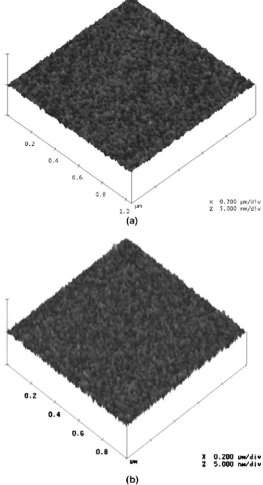
Take-off angles共TOAs兲 of 60 and 90° were used to measure the XPS spectra of surface and bulk HfO2thin films共Fig. 2兲. In Fig. 2, for all samples except the as-deposited sample, a distinct F 1s peak at 687 eV can be observed. The CF4plasma treatment processes are apparently introducing fluorine atoms into the dielectrics, as noted in the prior SIMS analysis. Furthermore, the F 1s peak of the sample with the longer CF4 plasma treatment 共5 min兲 displays a higher intensity when the TOA is 60°. This implies that the longer CF4 plasma treatment introduces more fluorine at the surface of the HfO2 thin films. In addition, the fluorine intensity was nearly identical in the bulk of HfO2 thin films, regardless of CF4 plasma treatment conditions共Fig. 2; TOA is 90°兲. Figure 3 shows the Hf 4f ESCA spectra of HfO2and fluorinated HfO2thin film. Two distinct peaks of Hf–O bonding, at 18.7 and 20.3 eV, were found in the as-deposited sample. Nevertheless, the as-as-deposited samples may also have large numbers of other types of bonding defects, which was not observed when the material is prepared. The TOA angles of 60 90° were also used to measure the XPS spectra. Compared to the Hf–O bonds in Hf 4f spectra of the HfO2thin film, the Hf 4f spectra of the fluorinated HfO2thin film is shifted roughly 0.43 eV共Fig. 3兲. This also shows the Hf–F bonding formation after CF4plasma treatment, as seen in Fig. 1 and 2. To investigate the plasma etching effect in HfO2thin film, we used AFM and ellipsometry to analyze the sur-face roughness and thickness of the HfO2thin film with and without CF4plasma treatment. Ellipsometry indicated that the thicknesses of as-deposited and fluorinated HfO2 thin films 共P-5兲 are 5.035 and 4.994 nm, respectively. These results imply that the CF4 plasma etching effect during the treatment of HfO2thin films is negligible. In addition, the root-mean-square共rms兲 variations of the surfaces of the as-deposited and fluorinated HfO2thin film共P-1兲, extracted from the AFM images, are 1.05 and 1.74 Å, respectively共Fig. 4a and b兲. Furthermore, the rms of the HfO2 thin film with 5 min of CF4 plasma treatment was only 2.03 Å. These results appear to show that the CF4plasma treatment did not damage the HfO2thin film during fluorinated HfO2thin film formation.
Figure 5 shows the current density vs gate voltage共J-V兲 charac-teristics of as-deposited and fluorinated HfO2 gate dielectrics. The gate leakage current of the samples after 700°C annealing increased due to dielectric film crystallization. In addition, the breakdown Figure 1. SIMS depth profile of MOS structure for fluorine oxygen,
hafnium, and silicon atom distribution. The fluorine atoms were accumulated mainly at the two interfaces of the gate-oxide films.
Figure 2. XPS analysis of the F 1s electronic spectra of as-deposited and
fluorinated samples, TOAs of 60 and 90°, respectively, where the F 1s peak is at 687 eV.
Figure 3. Hf 4f XPS spectra of as-deposited and fluorinated HfO2thin films, respectively. Take-off angles of 60 and 90° were used to measure the XPS spectra.
voltage of the fluorinated HfO2gate dielectrics was also improved 共Fig. 5兲. The inset in Fig. 5 depicts the close fit of all samples to the Frenkel–Poole model. The linear behavior is a further indication that the carrier transportation in both as-deposited and fluorinated HfO2 is F–P emission. The effective barrier heights 共⌽B兲 were much higher for the fluorinated HfO2 gate dielectrics, with and without PDA treatment 共inset, Fig. 5兲. In addition, the Schottky emission barrier共TaN/HfO barrier兲 was also calculated. Because the barrier height extracted from Schottky emission was larger than the trap energy extracted from F–P conduction, the F–P conduction mecha-nism would dominate over the Schottky emission.
Figure 6 shows the effective oxide thickness vs gate leakage current characteristics of HfO2gate dielectrics with and without CF4 plasma treatment and 700°C postdeposition annealing共PDA兲. The inset shows the C-V characteristics of all the samples. The thinner EOT extracted from C-V curves was obtained for the HfO2 gate dielectrics with CF4 plasma treatment and was further improved
after annealing at 700°C. The CF4 plasma treated HfO2films ap-peared to possess properties superior to those of the as-deposited samples, including thin EOT and low leakage current. However, the HfO2films, after 700°C PDA, still presented higher gate leakage current at the same EOT than the as-deposited samples, owing to the film crystallization discussed earlier.
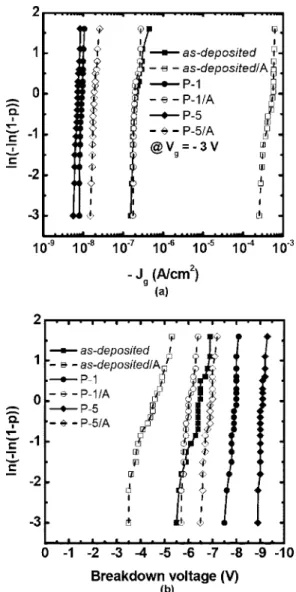
Figure 7 shows the Weibull distribution plots of the gate leakage current density at the gate voltage of −3 V and the breakdown volt-age for all samples. Both the performance and uniformity distribu-tion of the fluorinated HfO2gate dielectrics were superior to those of the as-deposited samples.
The normalized C-V hysteresis curves of the as-deposited and fluorinated HfO2gate dielectrics are shown in Fig. 8a and b, respec-tively. The C-V hysteresis of the as-deposited HfO2gate dielectrics was 1 V, but decreased to roughly 50 mV for the fluorinated HfO2 gate dielectrics 共P-5兲. According to the inner-interface trapping model,25 when the capacitor is biased at accumulation 共VG= −3 V兲, majority carriers 共holes for the p-type Si substrate兲 tunnel from p-Si substrate through the interfacial layer共IL兲 and are trapped at the inner-interface, as indicated in the inset band diagram in Fig.
Figure 4. AFM images of the surface of the HfO2thin films共a兲 without CF4 plasma treatment and共b兲 with CF4plasma treatment for 1 min.
Figure 5. C-V characteristics for the as-deposited and fluorinated HfO2gate dielectrics with and without PDA.共Inset兲 The F–P curve fit for all samples. The fluorinated HfO2gate dielectrics have a higher F–P barrier height, which increases as plasma treatment time increases.
Figure 6. The relationship between gate leakage current and EOT, extracted
from the C-V curves共inset figure兲 for all samples. The fluorinated HfO2gate dielectrics have lower leakage current and EOT.
8a. Furthermore, when the voltage is biased at the inversion region 共VG= 1 V兲, the trapped holes at the inner-interface will be de-trapped, while at the same time the minority carriers 共electrons兲 tunnel from the p-Si substrate and are trapped at the inner-interface. On the other hand, the shifted C-V curves are not parallel at inter-mediate and low voltages. A slight degradation of C-V curves in depletion region can be observed as indicated in Fig. 8a. As a result, the hysteresis phenomenon was contributed by both interface states and bulk trapping. However, for the fluorinated HfO2thin film, the number of holes and the number of electrons trapped at the inner-interface and some inner-interface states were reduced, owing to the F atoms incorporated into the HfO2 thin film 共Fig. 8b, inset兲. This indicates that hole trapping was observed in our HfO2thin film, a finding strongly supported by the negative flat band voltage shift during the C-V hysteresis measurement.
Figure 9 displays the Weibull distribution of C-V hysteresis for all samples. The C-V hysteresis was improved by increasing the CF4 plasma treatment duration. Of all the samples, the HfO2films with CF4 plasma treatment for 5 min, and rapid thermal annealing at 700°C for 30 s共P-5/A兲 exhibit the smallest C-V hysteresis, about 40 mV.
Figure 8. The C-V hysteresis characteristics for the共a兲 as-deposited and 共b兲
fluorinated HfO2gate dielectrics, respectively. The inset band-diagram ex-plains the charge trapping mechanism.
Figure 10. Arrhenius plots of leakage current density for the HfO2 and fluorinated HfO2gate dielectrics. The plots were obtained from the current-voltage characteristics at Vg = −3 V measured from 303 to 353 K.
Figure 7. The Weibull distribution of the共a兲 gate leakage current and 共b兲
breakdown voltage, for the as-deposited and fluorinated HfO2gate dielec-trics. A good distribution performance of the fluorinated HfO2gate dielec-trics was observed.
Figure 9. The Weibull distribution of the C-V hysteresis for all samples.
Only 50 mV C-V hysteresis was observed for the fluorinated HfO2 gate dielectrics.
2
age characteristics at VG= −3 V, measured at 303–353 K. The data fit to the relationship J⬁ exp共−Ea/kBT兲. The calculated values of the activation energies for the as-deposited sample and fluorinated samples are 0.28, 0.13共P-1兲, and 0.06 eV 共P-5兲, respectively. This apparently shows that the CF4plasma treatment effectively removed the dielectric vacancies, leading to a lower concentration of gener-ated traps.26The temperature dependence performance of the gate leakage current for as-deposited HfO2 gate dielectrics was more obvious, owing to the large concentration of generated traps共hole trapping兲, as illustrated in C-V hysteresis. The results of the decrease in activation energy共Fig. 10兲 indicate that the fluorinated HfO2gate dielectrics have a lower concentration of generated hole traps.
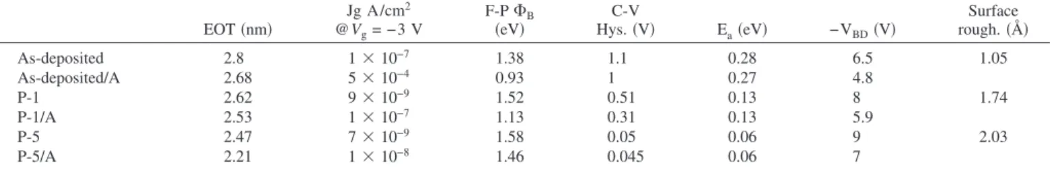
Table I summarizes the characteristics for all samples. The sur-face roughness of the HfO2 thin films was not degraded by CF4 plasma treatment. Furthermore, the fluorinated sample exhibits su-perior properties in EOT, leakage current, breakdown voltage, hys-teresis, and elimination of deep traps.
Conclusion
An approach to demonstrate the characteristics of fluorinated HfO2gate dielectrics formed by CF4plasma treatment was proposed and systematically studied. The fluorinated HfO2thin film exhibited superior C-V and I-V performance even after high-temperature an-nealing. Furthermore, charge trapping occurred in C-V hysteresis, while measurement of the fluorinated HfO2gate dielectrics was ef-fectively improved. This technology may be applicable to HfO2thin films for future ULSI applications.
Acknowledgments
The authors thank the National Science Council, R.O.C., for funding this research through grant NSC-94-2215-E-182-008.
Chang Gung University assisted in meeting the publication costs of this article.
2057共2001兲.
2. International Technology Roadmap for Semiconductors 2005 Update, The Semi-conductors Industry Association共2005兲.
3. J. C. Wang, D. C. Shie, T. F. Lei, and C. L. Lee, J. Appl. Phys., 98, 024503共2005兲. 4. C. S. Lai, W. C. Wu, T. S. Chao, J. H. Chen, J. C. Wang, L. Tay, and N. Rowell,
Appl. Phys. Lett., 89, 072904共2006兲.
5. J. C. Wang, D. C. Shie, T. F. Lei, and C. L. Lee, Electrochem. Solid-State Lett., 6, F34共2003兲.
6. C. H. Choi, S. J. Rhee, T. S. Jeon, N. Lu, J. H. Sim, R. Clark, M. Niwa, and D. L. Kwong, Tech. Dig. - Int. Electron Devices Meet., 2002, 857.
7. R. Choi, C. S. Kang, B. H. Lee, K. Onishi, R. Nieh, S. Gopalan, E. Dharmarajan, and J. C. Lee, VLSI Technical Symposium Digest, IEEE, p. 15共2001兲. 8. T. P. Ma, in Extended Abstracts of the Solid State Device and Materials, p. 30
共2004兲.
9. Z. Zhang, M. Li, and S. A. Campbell, IEEE Electron Device Lett., 26, 20共2005兲. 10. C. L. Cheng, C. Y. Lu, K. S. Chang-Liao, C. H. Huang, S. H. Wang, and T. K.
Wang, IEEE Trans. Electron Devices, 53, 63共2006兲.
11. C. S. Lai, W. C. Wu, J. C. Wang, and T. S. Chao, Appl. Phys. Lett., 86, 022905 共2005兲.
12. P. F. Lee, J. Y. Dai, K. H. Wong, H. L. W. Chan, and C. L. Choy, Appl. Phys. Lett., 82, 2419共2003兲.
13. M.-H. Cho, D. W. Moo, S. A. Park, Y. K. Kim, K. Jeong, S. K. Kang, D.-H. Ko, S. J. Doh, J. H. Lee, and N. I. Lee, Appl. Phys. Lett., 84, 5243共2004兲.
14. S. J. Rhee, C. Y. Kang, C. S. Kang, R. Choi, C. H. Choi, M. S. Akbar, and J. C. Lee, Appl. Phys. Lett., 85, 1286共2004兲.
15. C. S. Kang, H. J. Cho, K. Onishi, R. Nieh, R. Choi, S. Gopalan, S. Krishnan, J. H. Hari, and Jack C. Lee, Appl. Phys. Lett., 81, 2593共2002兲.
16. G. Q. Lo, W. Ting, D. L. Kwong, J. Kuehne, and C. W. Magee, IEEE Electron
Device Lett., 11, 511共1990兲.
17. P. J. Wright and K. C. Saraswat, IEEE Trans. Electron Devices, 36, 879共1989兲. 18. L. Vishnubhotla, T. P. Ma, H. H. Tseng, and P. J. Tobin, IEEE Electron Device
Lett., 14, 196共1993兲.
19. S. Lee and J. W. Park, J. Appl. Phys., 80, 5260共l996兲.
20. C. S. Lai, W. C. Wu, J. C. Wan, and T. S. Chaos, Extended Abstracts of the Solid State Device and Materials, p. 234共2005兲.
21. M. Inoue, S. Tsujikawa, M. Mizutani, K. Nomura, T. Hayashi, K. Shiga, J. Yugami, J. Tsuchimoto, Y. Ohno, and M. Yoneda, Tech. Dig. - Int. Electron Devices Meet.,
2005, 402.
22. K. Seo, R. Sreenivasan, P. C. McIntyre, and Krishna C. Saraswat, Tech. Dig. - Int.
Electron Devices Meet., 2005, 406.
23. Y. Mitani, H. Satake, Y. Nakasaki, and A. Toriumi, IEEE Trans. Electron Devices, 50, 2221共2003兲.
24. P. J. Wright and K. C. Saraswat, IEEE Trans. Electron Devices, 36, 879共1989兲. 25. J. C. Wang, S. H. Chiao, C. L. Lee, T. F. Lei, Y. M. Lin, M. F. Wang, S. C. Chen,
C. H. Yu, and M. S. Liang, J. Appl. Phys., 92, 3936共2002兲. 26. I. Rahat and J. Shappir, J. Appl. Phys., 76, 2279共1994兲.