Contents lists available atScienceDirect
Materials Science and Engineering B
j o u r n a l h o m e p a g e :w w w . e l s e v i e r . c o m / l o c a t e / m s e bInvestigation of GaN-based vertical-injection light-emitting diodes
with GaN nano-cone structure by ICP etching
H.W. Huang
a,b,∗, C.H. Lin
b, C.C. Yu
b, K.Y. Lee
b, B.D. Lee
b, H.C. Kuo
a,
S.Y. Kuo
c, K.M. Leung
d, S.C. Wang
aaInstitute of Electro-Optical Engineering, National Chiao Tung University, Hsinchu 300, Taiwan, ROC bLuxtaltek Corporation, Chunan, Miaoli 350, Taiwan, ROC
cDepartment of Electronic Engineering, Chang Gung University, Tao-Yuan 333, Taiwan, ROC
dDepartment of Computer and Information Science, Polytechnic University, Six Metrotech Center, Brooklyn, NY 11201, USA
a r t i c l e i n f o
Article history:Received 10 April 2008
Received in revised form 2 July 2008 Accepted 6 July 2008
Keywords:
Light-emitting diode (LED) Nano-cone
Inductively coupled plasma (ICP)
a b s t r a c t
The GaN-based thin-film vertical-injection LEDs (VLEDs) with GaN nano-cone structures are fabricated and presented. Under the process conditions of fixed Cl2/Ar flow rate of 10/25 sccm and ICP/bias power of
200/200 W, the GaN nano-cone structures are self-assembly formed with variable density of 1.5× 10⁷to
1.4× 109cm−2and variable depth of 0.56–1.34m when varying the ICP chamber pressure. At a driving
current of 350 mA and with chip size of 1 mm× 1 mm, the light output power of our thin-film LED with a specific GaN nano-cone structure reaches 224 mW which is enhanced by 160% when compared with the output power of conventional VLED. In addition, the corresponding light radiation pattern shows much higher light intensity due to the strong light scattering effect by the formed nano-cone structure.
© 2008 Elsevier B.V. All rights reserved.
GaN-based materials have attracted considerable interest in many optoelectronic device applications, such as light-emitting diodes (LEDs) and laser diodes (LDs). Recently, high brightness GaN-based LEDs has gradually invaded into the applications of out-door displays, traffic signals, LED-backlit liquid crystal displays and direct-view large area signage[1–3]. To further extend the appli-cation arm of GaN-based LED to projectors, automobile headlight and even general lighting, further improvement on optical power and light extraction efficiency are eagerly required. The thin-film LED structure is developed very recently and can be a promising candidate to achieve the goals. A well known thin-film GaN LED structure is fabricated by the process steps of removing sapphire using an excimer laser[4–6], and roughening revealed n-doped GaN [7]. Recently, we reported an increase in the extraction efficiency of GaN-based LEDs by surface roughening[8,9]. To improve the light scattering effect or extraction efficiency of a roughened surface, lots of methods of fabricating nanostructures on GaN surface have been reported, such as GaN nanorods using inductively coupled plasma reactive-ion etching (ICP-RIE) with nano-mask[10], growth of free dislocation InGaN/GaN MQW nanorod arrays by MO-HVPE [11], nanoporous GaN:Mg structure using photochemical etching (PEC)
∗ Corresponding author at: Institute of Electro-Optical Engineering, National Chiao Tung University, Hsinchu 300, Taiwan, ROC.
E-mail address:[email protected](H.W. Huang).
[12], and InGaN/GaN nanoposts using e-beam lithography[13]. To maximize the light scattering performance of nanostructure, in this paper, we report a simple technique of fabricating bundles of GaN nano-cone on GaN vertical-injection LEDs (VLEDs) epitaxial film, and the height and density of the corresponding GaN nano-cones are controllable by using ICP-RIE. Further, to demonstrate ultra-high brightness GaN-based LEDs, the electrical and optical characteristics of a thin-film VLED incorporated with a GaN nano-cone structure are presented.
Our prepared GaN LED wafer consists of a 50-nm thick of GaN nucleation layer grown at 550◦C, a 2-m thick of un-doped GaN buffer layer grown at 1050◦C, a 3-m thick of Si-doped n-GaN layer grown at 1050◦C, an unintentionally doped InGaN/GaN mul-tiple quantum well (MQW) of active region grown at 770◦C, a 50-nm thick of Mg-doped p-AlGaN electron blocking layer grown at 1050◦C, and a 0.2m thick of Mg-doped p-GaN contact layer grown at 1050◦C. The MQW active region consists of five periods of 3/7 nm-thick of In0.21Ga0.79N/GaN quantum well layers and bar-rier layers.Fig. 1is a schematic diagram for our GaN VLED with GaN nano-cone structures. The whole process steps are described as follows.
First, a transparent contact of Ni/Au (3/3 nm) layer, silver mir-ror, and bonding metal layer of Cr/Pt/Au (20/30/1000 nm) are deposited on p-GaN of our prepared LED wafer, respectively. Then deposited LED wafer is bonded onto a Cr/Pt/Au (20/30/1000 nm) coated p-type conducting Si substrate by commercial SUSS SB6e
0921-5107/$ – see front matter © 2008 Elsevier B.V. All rights reserved. doi:10.1016/j.mseb.2008.07.002
Fig. 1. A schematic diagram of a vertical-injection LED structure with GaN
nano-cone structure.
wafer bonder at bonding temperature of 350◦C and bonding pres-sure of 17 kg/cm2 for 120 min. Second, the sapphire substrate of bounded wafer is removed by a well known Laser Lift-Off (LLO) process. In our experiment, a KrF excimer laser at wavelength of 248 nm with pulse width of 25 ns is used. The incident laser with a beam size of 1.2 mm× 1.2 mm is incident from the polished back-side of the sapphire substrate onto the sapphire/GaN interface to decompose GaN into Ga and N2. In this LLO process, the beam size of KrF laser is larger than our desired size (1 mm× 1 mm) of LEDs, therefore, the laser irradiation on the interface of sapphire and GaN is rather uniform. Third, the sapphire-removed bounded wafer is dipped into HCl solution to remove the residual Ga on the u-GaN. In order to thin out the revealed n-GaN, the whole sapphire-removed wafer is etched with the etching condition of a gas mixture of Cl2/Ar = 10/25 sccm with the ICP source power,
bias power set at 200/200 W, and a chamber pressure of 2.5 mTorr with an approximate etching depth of 2m by ICP-RIE. Fourth, the associated mesas are etched further down to the Cr metal inter-face using SiO2etching mask by plasma enhanced chemical vapor deposition (PECVD) for single chip isolation and then used a buffer oxidation etchant (BOE) to remove the residual SiO2 layer. Fifth, a 0.5-m of SiO2 is deposited onto the wafer surface and then photo-lithography is used to define the passivation pattern after wet etching of SiO2 by a BOE solution. Sixth, a patterned Cr/Au electrode is deposited on n-GaN as the n-type contact layer and Cr/Au metal is deposited on Si substrate backside. Finally, under a gas mixture condition of Cl2/Ar = 10/25 sccm with the ICP source power, bias power set at 200/200 W, and etching time of 2 min with different chamber pressure for VLEDs, n-GaN nano-cone structures of various heights and densities are self-assembly formed when controlling the chamber pressure to be from 2.5 to 67.5 mTorr. The heights and densities of various nano-cone are estimated by a scan-ning electron microscope (SEM) (Hitachi FE-SEM S-5000).
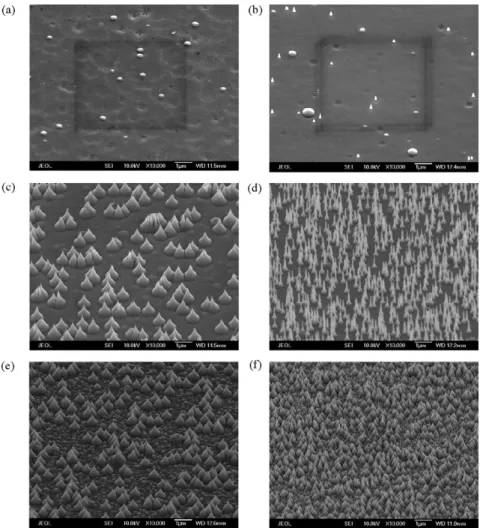
Fig. 2(a) is the SEM image with 30◦ tilted view angle, which shows a uniform etched surface without obvious GaN nano-cone structure when the chamber pressure is 2.5 mTorr. However, when the chamber pressure is increased to 10.0 mTorr, as shown in Fig. 2(b), the n-GaN nano-cones begin to be formed and the density of nano-cones increases as the chamber pressure keeps increasing. Fig. 2(c–f) shows the GaN surface morphologies at chamber pres-sures of 20.0, 37.5, 52.0 and 67.5 mTorr, respectively. Apparently, the GaN surface becomes to be randomly roughened when the pressure is beyond 52.0 mTorr.
Fig. 3. The density and depth of GaN nano-cone structures as a function of the
chamber pressure varies from 5 to 67.5 mTorr with Cl2/Ar flow rate of 10/25 sccm,
ICP/bias power of 200/200 W for 2 min of etching time.
We also calculate the mean height and density of the GaN nano-cone by SEM data as shown inFig. 3. The density of nano-cone increases from 1.5× 10⁷to 1.4× 109cm−2when the chamber pres-sure is increased from 5 to 37.5 mTorr, respectively. In addition, the height of the GaN nano-cones can reach a maximum of 1.34m with height/diameter ratio of 3 at 37.5 mTorr and is then gradually decreased due to lower plasma densities resulting from
recom-bination. The result suggests that the chamber pressure plays a major role on forming and controlling the height and density of GaN nano-cones. Although the exact mechanism of the formation of such nano-cone structures is not fully understood yet, it seems to be related to the crystalline quality of epitaxially grown GaN material and the capability of the ICP process of dissociating GaN bond. In general, MOCVD-grown GaN on a sapphire substrate is known to have high densities of dislocation and defect on the order of 108to 109cm−2because of a lattice mismatch between the GaN and sapphire substrate. These dislocations and defects tend to have weaker binding energy and could be easily dissociated by the ICP etching process leaving behind the rigid crystalline GaN region[14]. As for the increase in the nano-cone density when raising chamber pressure, it could be attributed to the degradation of the ICP dis-sociation ability at a higher chamber pressure[15,16]. According to Refs.[15,16], the plasma density is a strong function of the cham-ber pressure. As the chamcham-ber pressure is increased, the mean free path decreases and the collisional frequency increases. This tends to result in changes in both ion energy and plasma density which strongly influence the dissociation of GaN bonding during the ICP etching process.
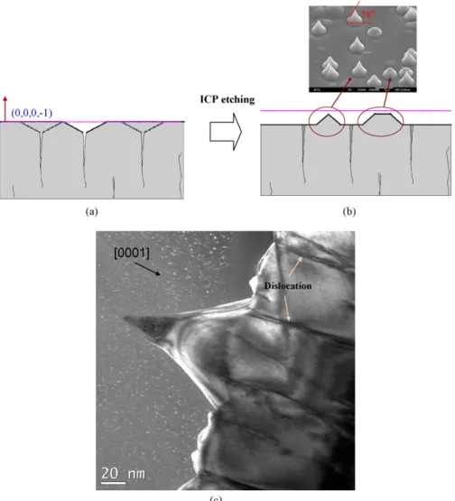
As we know, there are many dislocations in the GaN film for the lattice mismatch between the GaN film and sapphire substrate after LLO process as shown inFig. 4(a). Those dislocations are randomly revealed or hidden in the GaN film, and some of their distances are very near and others are very far. If the dislocation is hidden in
Fig. 5. (a) Current–voltage (I–V) and (b) intensity–current (L–I). (c) Room temperature EL spectra for the conventional VLED and VLED with GaN nano-cone structure.
the GaN film, it is easy to form the stacking faults on the front or top of the dislocation and induces the week binding. Therefore, as shown inFig. 4(b), at the beginning of the ICP etching process using a gas mixture condition of Cl2/Ar = 10/25 sccm with the ICP source power, bias power set at 200/200 W, chamber pressure at 30 mTorr, and etching time of 45 s, the cones with a tip can be formed at the spot where the distance of dislocations is near and the cones with a mesa will be formed at the spot where the distance of disloca-tions is far. However, the cones with a mesa are turned to be the cones with a tip when the etching depth of the GaN is over 1.5m (using n-GaN test sample for ICP etching). Those cones with a tip are randomly revealed on the GaN surface and the angle between the side plane and basal plane of the tip is around 58◦[17]. In addition, according to our experimental results, the distances between those cones with a tip are generally smaller than 2m. Therefore, there are two possible mechanisms for forming the cones with a tip or a mesa. One is the higher etching rate on the dislocation region than the rate on other regions; the other is the etching depth of n-GaN using dry etching process.
The high-resolution transmission electron microscopy (TEM) (JEOL, JEM-200CX) image of the VLED with GaN nano-cone illus-trated inFig. 4(c) shows the diameter and height of a GaN nano-cone are approximately 85 and 100 nm, respectively, using a gas mixture condition of Cl2/Ar = 10/25 sccm with the ICP source power, bias power set at 200/200 W, chamber pressure at 30 mTorr, and etch-ing time of 20 s. In that TEM image, the [0 0 0 1], direction is vertical to the plane of the cone, indicating that the [0 0 0 1] direction is a common growth direction of the GaN.
Fig. 5(a) shows the forward I–V curves for the VLEDs with and without GaN nano-cone structure. Suggest by the results of Figs. 2 and 3, we choose a gas mixture condition of
Cl2/Ar = 10/25 sccm with the ICP source power, bias power set at 200/200 W, chamber pressure at 37.5 mTorr, and etching time of 2 min for the device. It is found that the measured forward volt-ages under injection current of 350 mA at room temperature for the VLED with and without GaN nano-cone structure are 4.69 and 4.86, respectively. The slightly higher forward voltage of the VLED with GaN nano-cone structure can be attributed to the heating and charging damages during ICP-RIE etching process.Fig. 5(b) shows light output power as a function of forward DC current for the VLEDs with and without GaN nano-cone structure. At an injection current of 350 mA, the light output power of the conventional VLED and the VLED with nano-cone structure are 86 and 224 mW, respectively, indicating a factor of 2.6 is enhanced by the nano-cone structure. In addition, the corresponding wall plug efficiencies of the VLED with
Fig. 6. Far-field pattern of the conventional VLED and VLED with GaN nano-cone
and without nano-cone structure are 5.2% and 12.7%, respectively, which addresses a substantially improvement by the nano structure as well.Fig. 5(c) shows the typical room-temperature electrolumi-nescence (EL) spectra of the conventional VLEDs and the VLED with GaN nano-cone structure at a driving current of 350 mA, indicating that the InGaN-based MQW emission peaks of those two devices are both located at 453 nm.
To further study the influence of the nano-cone structure on the devices, we also measured the light output radiation patterns of the compared VLEDs packaged on transistor outline (TO)-cans at a driving current of 350 mA, as shown inFig. 6. It can be seen that the VLED with GaN nano-cone surface possesses much higher extrac-tion efficiency with a view angle about 136◦compared to the view angle of 122◦for the VLED without GaN nano-cone structure. This enhancement was attributed to the strong light scattering effect by the GaN nano-cone surface defined by ICP etching on our VLEDs.
In summary, GaN-based thin-film VLEDs with GaN nano-cone structure is designed and fabricated. We demonstrate a simple technique of fabricating GaN nano-cone structure of which the height and density are controllable using ICP-RIE. At a driving cur-rent of 350 mA and with chip size of 1 mm× 1 mm, the light output power and the wall plug efficiency of the VLEDs with a specific GaN nano-cone structure can achieve 224 mW and 12.7% which are increased by 160% and 144%, respectively, when compared with the results of the conventional VLEDs without nano-cone struc-ture. The corresponding light radiation pattern shows much higher light intensity due to the strong light scattering effect by the formed nano-cone structure.
References
[1] S. Nakamura, M. Senoh, S. Nagahama, N. Iwasa, T. Yamada, T. Matsushita, H. Kiyoku, Y. Sugimoto, Jpn. J. Appl. Phys. Part 2 35 (1996) L74.
[2] I. Akasaki, S. Sota, H.H. Sakai, T. Tanaka, M. Koike, H. Amano, Electron. Lett. 32 (1996) 1105.
[3] T. Mukai, M. Yamada, S. Nakamura, Jpn. J. Appl. Phys. Part 1 38 (1999) 3976.
[4] C.F. Chu, F.I. Lai, J.T. Chu, C.C. Yu, C.F. Lin, H.C. Kuo, S.C. Wang, J. Appl. Phys. 95 (2004) 3916.
[5] W.Y. Lin, D.S. Wuu, K.F. Pan, S.H. Huang, C.E. Lee, W.K. Wang, S.C. Hsu, Y.Y. Su, S.Y. Huang, R.H. Horng, IEEE Photon. Technol. Lett. 17 (2005) 1809.
[6] C.L. Chang, Y.C. Chung, C.Y. Liu, Electrochem. Solid-State Lett. 10 (2007) H344.
[7] T. Fuji, Y. Gao, R. Sharma, E.L. Hu, S.P. DenBaars, S. Nakamura, Appl. Phys. Lett. 84 (2004) 855.
[8] H.W. Huang, J.T. Chu, C.C. Kao, T.H. Hsueh, C.C. Yu, H.C. Kuo, S.C. Wang, Nan-otechnology 16 (2005) 1844.
[9] H.W. Huang, H.C. Kuo, J.T. Chu, C.F. Lai, C.C. Kao, T.C. Lu, S.C. Wang, R.J. Tsai, C.C. Yu, C.F. Lin, Nanotechnology 17 (2006) 2998.
[10] H.W. Huang, C.C. Kao, T.H. Hsueh, C.C. Yu, C.F. Lin, J.T. Chu, H.C. Kuo, S.C. Wang, Mater. Sci. Eng. B 113 (2004) 125.
[11] H.M. Kim, Y.H. Cho, H.S. Lee, S.I. Kim, S.R. Ryu, D.Y. Kim, T.W. Kang, K.S. Chung, Nano Lett. 4 (2004) 1059.
[12] C.F. Lin, J.H. Zheng, Z.J. Yang, J.J. Dai, D.Y. Lin, C.Y. Chang, Z.X. Lai, C.S. Hong, Appl. Phys. Lett. 88 (2006) 083121.
[13] H.S. Chen, D.M. Yeh, Y.C. Lu, C.Y. Chen, C.F. Huang, T.Y. Tang, C.C. Yang, C.S. Wu, C.D. Chen, Nanotechnology 17 (2006) 1454.
[14] J.A. Bardwell, J.B. Webb, H. Tang, J. Fraser, S. Moisa, Electrochem. Soc. Proc. 1 (2001) 193.
[15] S.J. Pearton, J.C. Zolper, R.J. Shul, F. Ren, J. Appl. Phys. 1 (1999) 86.
[16] R.J. Shul, C.G. Willison, M.M. Bridges, J. Han, J.W. Lee, S.J. Pearton, C.R. Abernathy, J.D. Mackenzie, S.M. Donovan, Solid-State Electron. 42 (1998) 2269. [17] T. Palacios, F. Calle, M. Varela, C. Ballesteros, E. Monroy, F.B. Naranjo, M.A.
Sánchez-García, E. Calleja, E. Mu ˜noz, Semicond. Sci. Technol. 15 (2000) 996.