Highly Reflective Ag
ÕLa Bilayer Ohmic Contacts to p-Type
GaN
I-Chen Chen,a,zYi-Dar Chen,aChih-Chien Hsieh,aCheng-Huang Kuo,band Li-Chuan Changc
a
Institute of Materials Science and Engineering and cDepartment of Optics and Photonics, National Central University, Jhongli 320, Taiwan
b
Institute of Lighting and Energy Photonics, National Chiao Tung University, Tainan County 711, Taiwan
A new Ag/La bilayer metal contact scheme has been developed for producing high reflectance and low contact resistivity ohmic contacts to p-GaN. An excellent reflectance of over 91% at 460 nm wavelength and low specific contact resistivity of 1.6 ⫻ 10−4⍀ cm2were obtained from Ag/La 共150/20 nm兲 contact annealed at 450°C for 1 min. The La overlayer was oxidized to
form La2O3when exposed to air, which effectively suppresses exposure of the Ag layer to oxygen atmosphere during annealing,
leading to a good ohmic contact with smooth surface morphology and high reflectance. Additionally, Ag/La contacts show excellent thermal stability after a long thermal annealing at 300°C in air ambient.
© 2011 The Electrochemical Society. 关DOI: 10.1149/1.3533673兴 All rights reserved.
Manuscript submitted October 13, 2010; revised manuscript received December 13, 2010. Published January 11, 2011.
Due to the better current spreading and efficient thermal dissipa-tion, GaN-based vertical-structure light-emitting diode共VLED兲 has been considered as a promising choice for high-power applications.1-3In the VLEDs, a high reflectance and low resistance p-GaN ohmic contact is essential to increase the light extraction and improve device performance. Silver共Ag兲 is a well-known highly reflective metal across the visible spectrum and could form ohmic contacts to p-GaN by annealing in air ambient. However, agglom-eration of Ag films occurred during annealing leads to degradation in electrical and optical properties.4,5Therefore, pure Ag films are not suitable to be used as p-GaN contacts for high-power VLEDs.
Regarding the physical origin of Ag agglomeration, two different mechanisms have been suggested, including surface diffusion to re-duce the total free energy and bulk diffusion of Ag atoms by oxygen–vacancy interaction.6,7Different Ag-alloys, such as Ag–Al, Ag–Cu, and Ag–Mg alloys, have been investigated as p-GaN con-tacts and proved to be able to suppress agglomeration, and thus result in better thermal stability due to the reduction in the oxygen– vacancy interaction.8-11The thermal stability of the Ag-based con-tacts could also be enhanced by depositing an overlayer on top of a Ag film.5,12In this paper, we present a new Ag/La bilayer metalli-zation scheme for p-GaN ohmic contacts. By employing Ag/La ohmic contacts, light reflectance, thermal stability, and surface mor-phology of the contacts are improved significantly. The effects of the La overlayer on electrical and optical properties of Ag contacts will be discussed.
Experimental
The 1m-thick Mg-doped GaN films used in this study were grown on c-plane sapphire substrates using metallorganic chemical vapor deposition共MOCVD兲. The carrier concentration determined by Hall measurements is about 3⫻ 1017cm−3. Prior to lithographic
patterning process, the as-grown GaN samples were ultrasonically degreased using acetone and methanol, and then rinsed in deionized water. The circular transfer length method共CTLM兲 patterns were defined by standard photolithography for specific contact resistance measurements. The CTLM pattern has a constant outer radius of 200m and the gap spacing between the inner and outer pads is varied from 5 to 45m. Before placing into the deposition chamber for metallization, all samples were dipped into a buffer oxide etch 共BOE兲 solution for 20 min in order to remove the surface oxide layer. Ag/La 共150/20 nm兲 bilayer contact patterns were deposited in sequence on the p-type GaN by electron-beam evaporation followed by the lift-off process. For comparison, a Ag共150 nm兲 film was also deposited on the p-type GaN as a reference. The CTLM contacts
were then annealed at temperatures ranging from 200 to 550°C for 1 min in air ambient using a rapid thermal annealing system. Current–voltage共I-V兲 characteristics of the contacts were examined using a semiconductor parameter analyzer 共HP 4145兲. A UV/Vis/ NIR spectrometer共JASCO V-670兲 was used to measure the reflec-tance of the Ag and Ag/La metal contact schemes deposited on quartz glass.
Results and Discussion
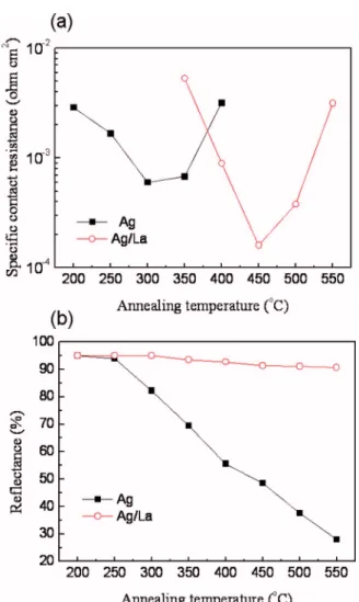
Figure 1ashows the specific contact resistance 共frequently re-ferred to as the specific contact resistivity兲 of Ag and Ag/La contacts before and after annealing as a function of the annealing tempera-ture. Both as-deposited metal contacts show nonohmic behavior. The specific contact resistances were measured for the Ag and Ag/La contacts which reveal ohmic behavior after annealing at tem-perature ranges of 200–400°C and 350–550°C, respectively. For the Ag contact, the lowest specific contact resistance of 6 ⫻ 10−4⍀ cm2 was obtained after annealing at 300°C, where the
specific contact resistance of the Ag/La contact is higher than that of the Ag contact. However, the Ag/La contact shows the lowest spe-cific contact resistance of 1.6⫻ 10−4⍀ cm2 after annealing at 450°C. The specific contact resistance of Ag and Ag/La contacts dramatically increases at annealing temperatures higher than 350 and 500°C, respectively, which implies degradation of the contacts. Figure1bshows the reflectance of both contacts at the wavelength of 460 nm at an annealing temperature range of 200–550°C. Both as-deposited Ag and Ag/La contacts reveal the same reflectance. The reflectance of the Ag contact degrades to 48.5% with annealing at 450°C, while the reflectance of the Ag/La contact is just slightly degraded over all annealing temperatures and showed high reflec-tance over 91% after annealing at 450°C. The reflecreflec-tance at 460 nm was chosen for the evaluation of light reflectance because the emis-sion wavelength of GaN LEDs for lighting applications is around that region of the spectrum. Figure 2 shows the reflectance as a function of wavelength for as-deposited and annealed Ag/La con-tacts. The reflectance of Ag/La contacts annealed at 450°C could maintain above 91% across the visible spectrum.
The surface morphologies of Ag and Ag/La contacts after an-nealing at 400°C by scanning electron microscopy 共SEM兲 are shown in Fig.3. The annealed Ag contact shows a very irregular and isolated island morphology, which could be explained on the basis of the high surface diffusion of Ag atoms in the oxygen-contained ambient.13The phenomenon of hole growth on Ag films is enhanced in the presence of oxygen and the island formation takes place by the holes joining together, leading to agglomeration. In the Ag con-tact, severe Ag agglomeration would strongly reduce the contact area and, thus, results in a poor specific contact resistance and a low light reflectance in reflective contacts at the high temperature region, z
E-mail: [email protected]
Journal of The Electrochemical Society, 158共3兲 H285-H288 共2011兲
0013-4651/2011/158共3兲/H285/4/$28.00 © The Electrochemical Society H285
) unless CC License in place (see abstract). ecsdl.org/site/terms_use
address. Redistribution subject to ECS terms of use (see 140.113.38.11
as indicated in Fig.1. Meanwhile, the Ag/La contact still exhibits smooth surface morphology and high reflectance even after anneal-ing at 450°C.
Based on the experimental results, the improvements in the spe-cific contact resistance and reflectance of annealed Ag/La contacts are explained. In order to investigate the interfacial reactions, X-ray photoelectron spectroscopy共XPS兲 analysis was carried out on both contacts. While the Ag layer is exposed directly to air during an-nealing in the Ag contact, the La layer, instead of Ag, is exposed in the Ag/La contact. Figure4shows the La3d and O1s XPS spectra of the La film at the Ag/La interface in as-deposited and annealed Ag/La contacts for studying the chemical states of lanthanum. Due to the spin–orbit interaction, La3d states split into two lines, 3d5/2
and 3d3/2, and each line has a double peak structure with a main
peak and a satellite peak. For the as-deposited La film, as depicted in Fig.4, the La3d5/2and La3d3/2features are resolved into two
dou-blets centered at 836.0 and at 852.8 eV with a spin orbit splitting of 16.8 eV, which is similar to that found in La2O3and suggests that the whole La layer could be oxidized to form a disordered La2O3
film by exposure to air at room temperature.14The O1s photoelec-tron spectra depicted in Fig.4also confirm the formation of a La2O3
overlayer. For the as-deposited sample, the peak at 530.5 eV in the O1s spectrum corresponds to O2−of the metal oxide.15
After anneal-ing at 450°C, the peak positions and shapes of La3d and O1s show no change, which implies no detectable formation of Ag–La solid solutions and intermetallic compounds. This indicates that La2O3 still remains as an overlayer after annealing, consistent with the result of the XPS depth profiles, as indicated in Fig.5. Because no oxygen XPS signal was observed inside the Ag contact共shown in Fig. 5兲, the Ag layer was not oxidized. For the annealed Ag/La
contact, the surface morphology is quite smooth without the forma-tion of holes, as shown in Fig.3b. Since Ag agglomeration could be enhanced by annealing in the oxygen-contained ambient,13we sug-gest that the overlaid La2O3 layer acts as a passivation layer to
reduce incorporation of oxygen into the Ag layer, and thus improve the reflectance in the annealed Ag/La contact. As shown in Fig.5, Ag indiffusion and Ga outdiffusion were observed at the interface between p-GaN and Ag in both contacts after the annealing process. The interdiffusion during annealing leads to the formation of Ag–Ga solid solution, which produces acceptorlike Ga vacancies beneath the contact, resulting in an increase in carrier concentration at the surface region and so the reduction of the Schottky barrier height.16 Ga outdiffusion could be enhanced by annealing in the oxygen-contained ambient due to the high reactivity of Ga with oxygen.17 For the Ag contact, therefore, the transition from Schottky to ohmic contact behavior occurs at annealing temperature as low as 200°C. Without excessive oxygen incorporation to enhance Ga outdiffusion, formation of Ag–Ga solid solution could still be promoted at a higher annealing temperature, and then results in ohmic behavior.18 Thus, compared with the Ag contact, the ohmic behavior was achieved for the Ag/La contact at a higher annealing temperature of 350°C and improved to reach a minimum specific contact resistance at 450°C. The improvement in the specific contact resistance for the Ag/La contact is speculated due to more Ag–Ga solid solution formed without reduction of the contact area共no Ag agglomeration兲 at a higher annealing temperature.
In order to evaluate the thermal stability of both contacts, we investigated the change of specific contact resistance and light re-flectance as a function of annealing time at 300°C. The specific contact resistance of each sample is normalized with the minimum contact resistivity共0兲 obtained after annealing at 300 and 450°C
for 1 min, respectively. Figure6shows the plot of normalized con-tact resistivity共t/0兲 versus annealing time. For the Ag contact, the
value oft/0drastically increased by a factor greater than 100 after
annealing for 50 min. However, the value of t/0 is almost
un-changed for the Ag/La contact after annealing for 120 min, which indicates that the La2O3overlayer could suppress the degradation of the Ag/La contact and result in better thermal stability.
Figure 1.共Color online兲 共a兲 Specific contact resistance of Ag 共150 nm兲 and
Ag/La 共150/20 nm兲 contacts as a function of annealing temperature in air ambient.共b兲 Light reflectance at 460 nm wavelength obtained from Ag and Ag/La contacts as a function of annealing temperature in air ambient.
Figure 2.共Color online兲 Light reflectance spectra of as-deposited Ag/La and
annealed Ag/La contact. Annealing was carried out at 450°C for 1 min in air.
H286 Journal of The Electrochemical Society, 158共3兲 H285-H288 共2011兲
H286
) unless CC License in place (see abstract). ecsdl.org/site/terms_use
address. Redistribution subject to ECS terms of use (see 140.113.38.11
Conclusion
In summary, a promising highly reflective and low resistance Ag/La ohmic contact for p-GaN has been demonstrated. The Ag/La contact shows a low specific contact resistance of 1.6 ⫻ 10−4⍀ cm2and high relative reflectance of over 91% at a
wave-length of 460 nm after annealing at 450°C in air. The excellent thermal stability in the Ag/La contacts is attributed to the formation of the overlaid La2O3layer on top of the Ag film during annealing, which serves as a passivation layer to prohibit the Ag
agglomera-Figure 3. SEM images of共a兲 Ag and 共b兲
Ag/La contacts to p-GaN annealed at 450°C in air ambient for 1 min.
Figure 4. 共Color online兲 XPS O1s and
La3d spectra taken at the Ag/La interface of the Ag/La bilayer contact before and after annealing at 450°C for 1 min in air ambient.
Figure 5. 共Color online兲 XPS atomic
depth profiles of Ag and Ag/La contacts before and after annealing. Ag contact was annealed at 300°C and Ag/La contact was annealed at 450°C. Both contacts were annealed under air atmosphere for 1 min.
H287
Journal of The Electrochemical Society, 158共3兲 H285-H288 共2011兲 H287
) unless CC License in place (see abstract). ecsdl.org/site/terms_use
address. Redistribution subject to ECS terms of use (see 140.113.38.11
tion. The results indicate that the Ag/La bilayer contact has high potential for applications of p-GaN contact in VLEDs.
Acknowledgments
This research was supported by National Science Council of Tai-wan.
National Central University assisted in meeting the publication costs of this article.
References
1. T. Fujii, Y. Gao, R. Sharma, E. L. Hu, S. P. DenBaars, and S. Nakamura, Appl. Phys. Lett., 84, 855共2004兲.
2. S.-J. Wang, K.-M. Uang, S.-L. Chen, Y.-C. Yang, S.-C. Chang, T.-M. Chen, and C.-H. Chen, Appl. Phys. Lett., 87, 011111共2005兲.
3. O. B. Shchekin, J. E. Epler, T. A. Trottier, T. Margalith, D. A. Steigerwald, M. O. Holcomb, P. S. Martin, and M. R. Krames, Appl. Phys. Lett., 89, 071109共2006兲. 4. J.-O. Song, J. S. Kwak, Y. Park, and T.-Y. Seong, Appl. Phys. Lett., 86, 062104
共2005兲.
5. H. W. Jang, J. H. Son, and J.-L. Lee, J. Electrochem. Soc., 155, H563共2008兲. 6. H. C. Kim, N. D. Theodore, and T. L. Alford, J. Appl. Phys., 95, 5180共2004兲. 7. J.-P. Crocombette, H. Monestrol, and F. Willaime, Phys. Rev. B, 66, 024114
共2002兲.
8. J.-Y. Kim, S.-I. Na, G.-Y. Ha, M.-K. Kwon, I.-K. Park, J.-H. Lim, and S.-J. Park, Appl. Phys. Lett., 88, 043507共2006兲.
9. J. H. Son, G. H. Jung, and J.-L. Lee, Appl. Phys. Lett., 93, 012102共2008兲. 10. Y. H. Song, J. H. Son, G. H. Jung, and J.-L. Lee, Electrochem. Solid-State Lett.,
13, H173共2010兲.
11. R. Kawai, T. Mori, W. Ochiai, A. Suzuki, M. Iwaya, H. Amano, S. Kamiyama, and I. Akasaki, Phys. Status Solidi C, 6, S830共2009兲.
12. H. W. Jang, J. H. Son, and J.-L. Lee, Appl. Phys. Lett., 90, 012106共2007兲. 13. S. K. Sharma and J. Spitz, Thin Solid Films, 65, 339共1980兲.
14. J. B. Cheng, A. D. Li, Q. Y. Shao, H. Q. Ling, D. Wu, Y. Wang, Y. J. Bao, M. Wang, Z. G. Liu, and N. B. Ming, Appl. Surf. Sci., 233, 91共2004兲.
15. M. Copel, E. Cartier, and F. M. Ross, Appl. Phys. Lett., 78, 1607共2001兲. 16. H. W. Jang and J-.L. Lee, Appl. Phys. Lett., 85, 5920共2004兲.
17. H. W. Jang, S. Y. Kim, and J.-L. Lee, J. Appl. Phys., 94, 1748共2003兲. 18. H.-K. Kim, M.-S. Yi, and S.-N. Lee, Thin Solid Films, 517, 4039共2009兲.
Figure 6.共Color online兲 Comparison of t/0ratios for Ag and Ag/La
con-tacts as a function of annealing time at 300°C in air ambient.
H288 Journal of The Electrochemical Society, 158共3兲 H285-H288 共2011兲
H288
) unless CC License in place (see abstract). ecsdl.org/site/terms_use
address. Redistribution subject to ECS terms of use (see 140.113.38.11