Abstract—Due to the benefits of Schottky diodes, 0.18- m
CMOS technology is being promoted for millimeter wave applica-tions. In this paper, 60-GHz dual-conversion down-/up-converters using Schottky diodes are realized by using 0.18- m foundry CMOS technology. A CoSi –Si Schottky diode, fabricated on a lower doped N-well by blocking the threshold voltage ad-justment implant, has a lower reverse leakage current and a better ideality factor. Thus, it is ideal for the 60-GHz sub-har-monic mixer design. Two new types of Schottky-diode mixers, a down-conversion sub-harmonic mixer with a dual-band lump-dis-tributed phase-inverter rat-race coupler and an up-conversion sub-harmonic mixer with a trifilar transformer, are realized and employed at the high-frequency conversion stage of the dual-conversion architecture to achieve small size and broadband isolations. The silicon-based Schottky diode with a low turn-on voltage offers great advantage in LO pumping power, especially for an antiparallel diode pair structure. In our Schottky-diode sub-harmonic mixers, the required LO power is only 1 dBm. The dual-conversion down-converter achieves 5-dB conversion gain
and 19 dB noise figure under and mA,
and the dual-conversion up-converter, with and mA, attains greater than 40-dB sideband rejection and 1 dB conversion gain over the whole 60-GHz bandwidth.
Index Terms—Converter, dual conversion, mixer,
phase-in-verter rat-race coupler, Schottky diode, single-sideband rejection, sub-harmonically pumped mixer, trifilar transformer, 0.18- m foundry CMOS technology, 60-GHz.
I. INTRODUCTION
A
60 GHz millimeter-wave system with unlicensed 7-GHz bandwidth conspicuously stands out in short-range high-data-rate applications, such as wireless personal area network (WPAN) and high-definition multimedia interface (HDMI). In 2004, the first CMOS 60-GHz amplifier was suc-cessfully demonstrated in standard 0.13- m CMOS technology, beginning 60-GHz transmission using the CMOS-based IC [1]. Subsequently, different architectures for receivers, transmit-ters and transceivers [2]–[16] were proposed and came into Manuscript received December 11, 2011; revised January 14, 2012; accepted January 23, 2012. Date of publication March 21, 2012; date of current ver-sion May 25, 2012. This work is supported in part by National Science Council of Taiwan, Republic of China under Contracts NSC 98-2221-E-009-033-MY3, NSC 99-2221-E-009-049-MY3 and NSC 98-2218-E-009-008-MY3, and in part by MoE ATU Program under Contract 95W803.The authors are with the Department of Electrical Engineering, National Chiao Tung University, Hsinchu 300, Taiwan (e-mail: onionpie.cm94g@nctu. edu.tw; [email protected]).
Color versions of one or more of the figures in this paper are available online at http://ieeexplore.ieee.org.
Digital Object Identifier 10.1109/TMTT.2012.2189412
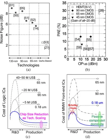
fruition by using standard advanced CMOS and SiGe HBT processes. However, fully-CMOS-based designs still encounter great difficulties in term of noise and power performances. Fig. 1(a) shows the comparison of stand-alone 60-GHz LNAs using 130-nm, 90-nm, 65-nm CMOS and III-V compound technologies. The noise figure of 60-GHz CMOS-based LNAs are above 5 dB while the III-V compound LNAs has the noise figure smaller than 3-dB due to the superior device noise prop-erty. The best III-V compound LNA [27] is based on 0.1- m InP heterojunction FETs and provides 2-dB NF and 23-dB gain with drain current of 8 mA at , thanks to the minimum device NF of 0.6 dB at 60-GHz. Thus, the III-V compound technologies are very attractive for the 60-GHz LNA design. For entire 60 GHz receivers, the noise figure (NF) of a 130-nm CMOS receiver [3] is up to 12.5 dB while 90-nm CMOS receivers [5]–[13] achieve a better NF of 5.5 8 dB. Recently, 65-nm [14], [15] or 45-nm [16] CMOS technology has also been devoted in the 60-GHz transmission. To date, the noise figures of the 65-nm and 45-nm CMOS receivers are 5.5 7 dB and 6 8 dB, respectively. The receiver noise figure improves slightly as the device scales down. Moreover, a 60-GHz power amplifier (PA) is also a key component because the output power of PAs has a great impact on the maximum transmission distance especially due to the high path loss at 60 GHz. The power amplifier does not prefer the CMOS scaling rule and PAE becomes even lower for the more advanced technology node due to lower breakdown voltage. A survey of the state-of-the-art 60-GHz PAs using advanced CMOS and III-V compound technologies is shown in Fig. 1(b). Compared with III-V compound technologies, standard CMOS PAs have lower PAE [54]–[58], and PAE and obviously decrease as the CMOS device is scaled down.
The scaling rule has caused both chip size shrinkage and steady reductions in IC manufacturing costs. Research and development (R&D) costs were never a concern and could easily be accounted for in the manufacturing stage in the past. However, R&D costs recently have become an issue as the transistor size of the CMOS process approaches the photolithography limit. In millimeter-wave IC design, much iteration is unavoidable due to inaccurate device modeling and high process variation, greatly aggravating R&D costs. Nowadays, 60-GHz radio is implemented in the phased-array transceiver format to avoid the signal blocking during trans-mission. An inefficient CMOS power amplifier becomes a severe problem in the 60 GHz beam-forming system because PAs and LNAs consume the most of chip area and the power 0018-9480/$31.00 © 2012 IEEE
Fig. 1. (a), (b) the superior capabilities of III-V compound technology in the 60-GHz noise and power performances, and the cost issue in (c) logic ICs and (d) millimeter-wave front-end ICs as a function of R&D and manufacturing phases for different CMOS generations.
consumption. Passive components, used in millimeter-wave transceiver, occupy a large percentage of the chip and cannot be scaled down by using advanced CMOS technology [6]. Thus, the phased-arrayed transceiver size does not shrink sufficiently as the scaling rule proceeds due to the inefficient CMOS PAs. As shown in [29], the size of LNAs and PAs of 60-GHz RX and TX is more than 80% of total die area mm . It is noticeable that the quarter-wavelength-based matching networks of PAs and LNAs occupy the most of chip area. The cost of the fully integrated CMOS phased-array transceiver is not low. Figs. 1(c) and 1(d) illustrate the costs of the logic ICs and millimeter-wave front-end ICs as a function of the R&D and manufacturing phases, respectively. The high R&D expense forms a barrier to product development. In Fig. 1(c), the high R&D costs of an advanced CMOS technology may still be covered for the logic IC product because of lower manufacturing cost by the device scaling rule. However, that is not the case for the millimeter-wave IC product because the scaling rule does not considerably decrease the manufacturing cost, as shown in Fig. 1(d).
While most of other researches follow the CMOS scaling rule and employ advanced CMOS technologies for the 60-GHz application, an alternative solution for the 60 GHz transceiver by simultaneously incorporating the advantages of III-V com-pound semiconductors and low-cost standard CMOS process is proposed and illustrated in Fig. 2. The use of external LNA/PA in III-V compound technologies is desirable because the
re-sulting 60-GHz phased-array transceiver based on our proposed approach is expected to have much less LNAs and PAs for the same EIRP (Effective Isotropic Radiation Power) and sensi-tivity achieved by advanced CMOS technologies. The reduction of power consumption makes the 60 GHz transceiver based on our approach possible for portable applications. In this paper, the first 60 GHz Schottky-diode-based front-end including up-and down-converters are demonstrated in a 0.18- m foundry CMOS process.
The Schottky diode, a majority-carrier device, has no minority storage effect and thus possesses very high-speed response for mixing and rectification. Among the GaAs-based technologies, Schottky-diode mixers have matured [17]. How-ever, little attention has been paid to the silicon processes because of the absence of Schottky diodes in a standard CMOS process. A 12-GHz down-converter using silicon Schottky diodes was demonstrated using bipolar technology with an extra processing step for Schottky diodes [18]. In 1996, the first experimental work to form Schottky diodes without an extra processing step in a foundry CMOS process was demonstrated by arranging the layout layers appropriately [19]. The initial rectifying effect of the Schottky diodes was limited to 600 MHz, possibly due to the long wire bonding used in the measurement setup. Until 2005, Schottky diodes with a cut-off frequency be-yond several hundred GHz were developed in standard CMOS [20]. The Schottky diodes based on the standard silicon process offer superior frequency conversion, and thus key components such as signal detectors [22], [26], frequency doublers [25], and mixers [24] have been implemented in the millimeter-wave regime. These results [22], [25], [26] shed light on the suit-ability of Schottky diodes in millimeter-wave applications using foundry CMOS process. The Schottky diode, like a catalyst, significantly reduces the R&D cost barriers shown in Fig. 1(d) and makes a 60-GHz transceiver with 0.18- m CMOS technology possible. However, no millimeter-wave transceiver based on the Schottky diodes has been reported to date.
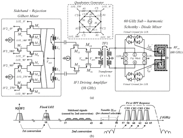
A direct conversion requires accurate quadrature signal generation directly at the same frequency of RF signals. Fully integrated transceivers, based on the direct conversion archi-tecture, have been successfully demonstrated below 5 GHz be-cause IQ signal generation is less sensitive to the parasitic ef-fects of the practical layout. When the channel bandwidth ap-proaches several GHz at the millimeter-wave frequency, it be-comes difficult to generate a precise, wideband IQ signal at 60 GHz. Thus, as discussed later in this paper, a dual-conver-sion architecture is employed to accomplish the band selec-tion and quadrature generaselec-tion in two separate steps. As shown in Fig. 2, the block diagrams for the 60-GHz dual-conversion up-/down-converters are depicted inside the dashed-square area. A precise IQ signal is generated by a fixed quadrature at low-frequency conversion while channel selection is achieved by sweeping at high-frequency conversion. The dual con-version consists of a high-frequency concon-version using the mi-crowave/millimeter-wave design approach and a low-frequency conversion using the analog design approach. For the higher-frequency conversion, a dual-band lump-distributed phase-in-verter rat-race coupler and a compact trifilar transformer to-gether with antiparallel diode pairs (APDPs) are proposed for
Fig. 2. Block diagram of the demonstrated dual-conversion up-/down-converters using Schottky diodes in 0.18- m standard CMOS technology for a 60 GHz transmission system.
Schottky-diode sub-harmonic down-conversion and up-conver-sion mixers (SHMs), respectively. The SHMs reduce the frequency to one-half of a fundamental mixer, and thus alleviate the difficulty of millimeter-wave generation with 0.18- m CMOS technology. The proposed SHM topologies provide in-herent cancellations among all ports of SHMs to achieve broad-band isolations. For lower-frequency conversion, analog mixers such as resistive and Gilbert mixers are employed due to size concern. There is a trade-off in designing frequency. In consideration of the problem of image/sideband signal at the high-frequency conversion, designed at higher frequency to facilitate the image/sideband signal suppression is preferred. However, the gain requirement for amplifiers sets an upper limit. In this paper, frequency is set at 10 GHz for 0.18- m CMOS technology. The image/sideband signal is 20 GHz away from the desired RF band of 57 66 GHz and can be easily filtered out by not only the bandpass response of the 60-GHz LNA/PA but also the preceding RF bandpass filter.
This paper is organized as follows. In Section II, a Schottky diode with small leakage current and good ideality factor is pre-sented. The properties of Schottky diodes, extracted from the S-parameter measurement, are characterized and discussed for the 60-GHz SHM design. Circuit implementations and measure-ment results of the demonstrated 0.18- m CMOS 60-GHz dual-conversion down-/up-converters are presented in Sections III and IV, respectively. Section V contains the conclusions of this paper.
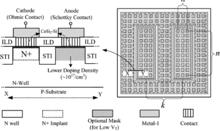
II. SCHOTTKYDIODEWITHLOWERDOPINGDENSITY IMPLEMENTED IN AFOUNDRYCMOSPROCESS
In the silicon-based technology, a thermal stable cobalt-sili-cide Schottky contact is formed by directly depositing metals on n- or p-wells with subsequent thermal silicidation. This is a well-known method for implementing Schottky contacts [19]–[21]. However, the default doping density of the n-well, defined by layer mask, is equivalent to that of the
nominal pMOS device in a TSMC 0.18- m
standard CMOS process. Here, represents the threshold voltage. The doping density needs to be adjusted for different generations of CMOS technology. In an advanced process, higher doping density is required, but this also affects the reverse leakage current and ideality factor of the Schottky contact. In the standard TSMC 0.18- m CMOS process, there are two types of n-wells with different doping densities for
high and low devices. Here,
an optional mask for low , which blocks pMOS threshold
Fig. 3. Cross section and layout of the Schottky diode with low-doping density implemented in 0.18- m foundry CMOS technology.
voltage adjustment implant in the well region, is used here to reduce the doping density of the n-well underneath the contact metal.
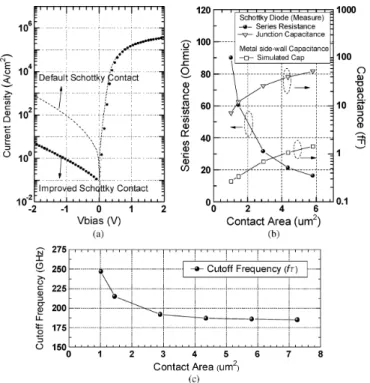
The contact number of Schottky diode is determined by the product of rows (m), columns (n), and fingers (k), as illustrated in Fig. 3. Each contact size is m and the spacing between contacts is 0.28 m complying with the minimum spacing in the design rule. The measured ideality factor of the
Schottky diode with is around
1.12, and its leakage current of 0.86 A/cm at
is two-order magnitude smaller than that without the optional mask, as shown in Fig. 4(a). The reverse avalanche breakdown voltage, barrier height and built-in voltage are 11 V, 0.53 eV and 0.4 V, respectively. Based on the standard C–V measurement, the doping density is on the order of cm . Here, a Schottky diode with low built-in voltage offers great advan-tages for the power design, especially in an antiparallel diode pair (APDP) SHM. Since it is infeasible to bias the diodes in an APDP structure, the required pumping power depends almost entirely on the diode’s built-in voltage. Compared with GaAs-based Schottky diodes with 0.7-V built-in voltage, APDP SHMs in CMOS technology at millimeter-wave frequency has a great advantage in term of driving power.
Fig. 4(b) shows the series resistances and junction ca-pacitances of the Schottky diodes with different sizes. The numbers of Schottky contact number are (I)
and (II)-(IV) 4 , as
illustrated in Fig. 3. The anode is surrounded by the cathode to reduce the access resistance. and are extracted from
Fig. 4. (a) Comparison of the measured I-V, and (b) the series resistance/junc-tion capacitance/metal side-wall capacitance and (c) cut-off frequency of the improved Schottky diode.
two-port S-parameter measurements at zero bias and the para-sitic effect of GSG pads is calibrated out in the parameter ex-traction. Measured S-parameters at 25 GHz are used. As shown in Fig. 4(c), the Schottky diode with contact number of
and the area of 0.726 m has the highest cutoff frequency, , of 250 GHz because the access resis-tance is minimized when the overall diode shape is close to a square shape. As the diode size increases, the cutoff frequency decreases until it finally starts to be stabilized at 185 GHz for diodes with contact number of . The cutoff frequency of a Schottky diode, determined by the resistance and capaci-tance, obviously increases for diodes with fewer rows, columns and fingers because the effect of access resistance is alleviated. It is expected that a diode with a single contact should achieve very high cutoff frequency. In the literature, diodes with a single
contact of m and m can reach the
cutoff frequencies of 400 GHz and 1.5 THz for 0.18 m [21] and 0.13 m [22] CMOS foundry processes, respectively. However, APDP configuration is used for our SHM design. The n-well ca-pacitance behaves as a shunt capacitor to the ground in an APDP configuration and thus can destroy the APDP high frequency performance such as matching and linearity [23]. For example, severe high frequency performance degradation has been ob-served for the single contact diode of m with the capacitance of 7.3 fF while the n-well to substrate capacitance is 41 fF [23]. The effect of the n-well capacitance on the high frequency is pronounced for diodes with small contact areas. Thus, a large contact area diode with a higher ratio of diode ca-pacitance to n-well caca-pacitance is employed to alleviate the no-torious n-well capacitance effect in this paper. Diodes with the contact number of are employed in this paper despite of a lower cut-off frequency. Each Schottky diode used in the APDP of the SHMs only works below 30 GHz, and the speed
of all test-keys is high enough for our circuit design. More-over, the simulated metal side-wall capacitances of the struc-tures (I)-(V), shown in Fig. 4(b), are 0.26, 0.34, 0.7, 1, 1.44 fF, respectively. Compared with of each Schottky diode, the metal side-wall capacitance only contributes less than 4% and has a small impact on the cut-off frequency. For example, the cut-off frequency of the structure (I) increases from 250 GHz to 260 GHz after subtracting the side-wall effect. Thus, the degra-dation on conversion gain at 60 GHz by the side-wall capaci-tance is negligible and much smaller than 0.5 dB from simula-tion.
In general, a diode with large is chosen for a narrow-band mixer to minimize the series resistance effect. The large can be formed by connecting the small devices with better in parallel if a higher conversion gain is needed despite of a larger device area. However, the effect of the n-well capacitor on APDP also sets a lower limit on the small device size in our work. A wideband mixer should use a diode with a small to alleviate the capacitive loading effect caused by the diode. But, its high series resistance degrades conversion efficiency and re-quires a larger driving power because of the difficulty in impedance matching. The trade-off exists in the diode-size se-lection for mixer design.
III. THEDEMONSTRATED60-GHz DUAL-CONVERSION DOWN-CONVERTER
The 60 GHz dual-conversion down-converter demonstrated in this research is composed of an SHM driven by the signal (first ), the first intermediate-frequency ampli-fier, a resistive mixer driven by the signal (second ), a wideband amplifier , and a quadrature generator as shown in Fig. 5(a). The frequency planning of the dual-conver-sion is illustrated in Fig. 5(b). It is easy to fix the frequency at the most accurate point of the IQ generator to obtain a precise baseband IQ output while the designated RF channel is selected by tuning the frequency. Here, the signal is tuned between 47 54 GHz and the signal is fixed at 10 GHz. In the high-frequency conversion, the silicon Schottky-diode SHM with low turn-on voltage facilitates the buffer amplifier de-sign. In this section, each stage of dual-conversion down-con-verter in Fig. 5(a) is presented and discussed in detail.
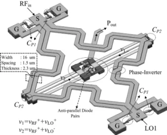
A. 60-GHz Sub-harmonically Pumped Mixer Using Dual-Band Lumped-Distributed Phase-Inverter Rat-Race Coupler
The first stage in the dual conversion is a 60-GHz SHM, which includes a dual-band phase-inverter rat-race coupler and two Schottky-diode mixer cells in APDP configuration, as shown in Fig. 6. The coupler merges an divider and an balun into one passive component to reduce the area necessary for SHM. An in-phase/out-of-phase signal is generated from the port while the two APDPs are series-connected between the remaining two ports as shown in Fig. 5(a). The in-phase/out-of-phase signal is always maintained for all fre-quencies because the physical paths from the ports to the other two outputs are equal in geometry for the phase-in-verter rat-race coupler. The balanced LO signals are achieved by a phase-inverter. The size of the phase-inverter in IC process
Fig. 5. (a) Schematic and (b) frequency planning of the 60-GHz dual-conversion down-converter by using Schottky diodes in 0.18- m CMOS technology.
Fig. 6. 3D view of the 60 GHz sub-harmonically pumped mixer using a dual-band lumped-distributed phase-inverter rat-race coupler in 0.18- m CMOS technology.
is a small proportion of the transmission line, and thus has a slight influence on the LO phase accuracy.
The output IF signal is taken from the virtual ground of the signals, formed at the middle point of two series connected APDPs, to achieve a good broadband -to-isolation. There are good broadband isolations between the RF and LO ports due to the intrinsic isolation property of the wideband four-port coupler. The APDP structure inherently possesses an even-harmonic rejection, enabling it to achieve
good broadband -to- and -to- isolations.
Here, the rat-race coupler must handle and signals at
two widely separate frequencies for the SHM. The signal ranges from 57 to 66 GHz, while the signal covers 23.5–28 GHz. The bandwidth of a phase-inverter rat-race coupler is de-termined by the input matching instead of the magnitude/phase imbalance. Thus, we design the return-loss as a dual-band, and two matching dips can be arranged by adjusting the equivalent transmission-line impedance of each arm of the phase-inverter rat-race coupler [30], [31].
As expressed in (1), is the normalized equivalent character-istic impedance of a coplanar stripline transmission line of the phase-inverter rat-race coupler and
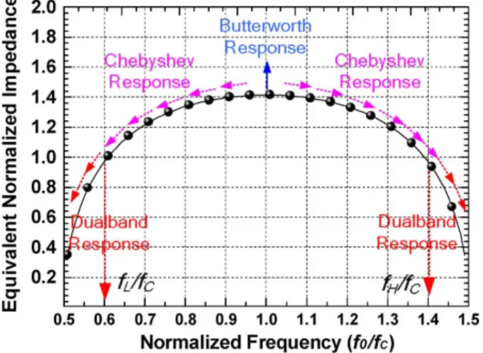
(1) and represent the frequencies of the matching dips and the center frequency of the lumped-distributed phase-inverter rat-race coupler, respectively. The spacing of the two split matching dips is extended when the equivalent characteristic impedance is continuously reduced, as shown in Fig. 7. It is the well-known Chebyshev-response design [31]. Although the wider bandwidth is realized by choosing lower character-istic impedance, there exists a trade-off between bandwidth and return-loss magnitude at . The limitation of a Chebyshev band-broadening technique is determined by the acceptable return loss at the center frequency of [32] (e. g. 10 dB in general case). As the characteristic impedance decreases further, a dual-band bandwidth response forms. The dual-band response, as shown in Fig. 5, is desired since only
Fig. 7. Bandwidth and characteristic impedance design of a phase-inverter rat-race coupler.
return-loss bandwidth near and RF frequencies needs to be covered for a sub-harmonic mixer design. The ratios of the two matching points to the center frequency of
and are designed to be 1.4 and 0.6.
and are the center frequencies for the
and bands, respectively. Here, a lump-distributed tech-nique, shunting capacitors at each port, is incorporated with the Chebyshev band-broadening technique to simultaneously achieve wide bandwidth and size reduction [33]. The equivalent characteristic impedance of the lumped-distributed transmis-sion line of each arm is around 45 for the desired ratio of and , in which the characteristic impedance of the coplanar stripline transmission line is designed as 55 by setting the spacing and width of metal-6 to 1.5 m and 16
m, respectively. Because the junction capacitance from the APDP, contributing to the size reduction, is not negligible, the shunting capacitance at both RF and LO ports is larger
than that of the other two ports. and are 40
fF and 25 fF, respectively. The phase-inverter rat-race coupler shown in Fig. 6 is directly implemented on the silicon substrate. Compared with the transmission line formed by interconnect metals and interlayer dielectrics, a coplanar stripline directly on the silicon substrate has a shorter effective wavelength due to its higher silicon dielectric constant , while the inter-metal dielectric has a smaller dielectric constant of 3.8 4. For a distortionless transmission line, energy is equally lost to the substrate and metal lines because of the equality condi-tion between R/L and G/C, and size reduccondi-tion by the dielectric constant still holds true as the case of a lossless transmission line. Distortionless transmission theory and concept for passive component miniaturization is developed in the appendix-B of our previous work [32]. High silicon dielectric constant has a great benefit in size shrinkage when implementing a microwave component directly on silicon substrate. The length of each arm in the lumped-distributed phase-inverter rat-race coupler
at is only 510- m. By winding the arms,
the phase-inverter rat-race coupler can be further compacted to a square with sides of 400 m in length, and the practical size of a stand-alone SHM is only 0.16 mm as shown in Fig. 8. Finally, from the EM simulation, the LO amplitude and phase
Fig. 8. Die photograph of the 60 GHz dual-conversion down-converter using 0.18- m CMOS technology.
errors over the whole operating frequency keep within 0.5 dB and 1 degree. The pure loss of the phase-inverter rat-race coupler is 5 6 dB.
B. Intermediate-Frequency Amplifier , Second-Stage Mixer, Wideband Output Buffer and Quadrature Generator
After the first conversion, the noise figure caused by the second conversion must be low enough to achieve an acceptable noise figure for the 60 GHz dual-conversion down-converter. Our goal is to have the overall noise figure of dual conversion below 20 dB based on the gain and noise figure of GaAs-based LNAs at 60 GHz. The first stage Schottky-diode SHM has a conversion loss of 15 dB. It means that the noise figure of the subsequent stage, including the intermediate-frequency amplifier, the second stage resistive mixer and the wideband
output buffer, must be lower than 5 dB at .
A topology with low noise figure and high gain, as shown in Fig. 5(a), is chosen for the amplifier. The amplifier consists of a common source stage with the source degeneration inductor of for simultaneous noise and gain match and a subsequent cascode stage for gain boosting. Here, the gain of the amplifier is designed to be around 18 20 dB to suppress the noise caused by the resistive mixer. The bandpass response of the input matching network of the amplifier suppresses the leakage signal. A 25-dB reduction in the leakage signal is obtained in simulation. At the output load of the amplifier, a single-to-differential transformer is employed for ac coupling, dc blocking, balanced-signal generation, and impedance transformation. The primary-coil inductance combined with the parasitic capacitance of the cascode device, , forms an LC tank at , and the sec-ondary-coil inductance resonates out the parasitic capacitance at the source of the resistive mixer. The transformer is de-signed with a turn ratio of two to transfer the high output impedance of the cascode stage to the low input impedance of the double-balanced resistive mixer. The transformer has a coupling factor of 0.7 while the primary and secondary inductances are 1.62 nH and 0.62 nH, respec-tively. The peak of quality factor is designed as closely as possible to . The maximum quality factor of the primary coil is 7.8 at of 8.5 GHz while the quality factor at 10 GHz is 7.5. The maximum quality factor of the secondary coil is 6.9 at of 10.3 GHz. To generate IQ baseband signals
Fig. 9. Measured and simulated RF/LO reflection coefficient of the miniature dual-band rat-race coupler of the 60-GHz dual-conversion down converter using 0.18- m CMOS technology.
at the low-frequency conversion stage, a poly-phase shifter is employed at the ports of the 10-GHz double-balanced resistive mixers. As shown in Fig. 5, a two-stage poly-phase shifter is cascaded to reduce the process variation, and the pole frequencies of the first and two stages are chosen at 11.8 and 8.2 GHz. A 38% bandwidth is covered. The poly resistor of
and MIM cap of have the values of 190
(560 ) and 60 fF (30 fF), respectively. is designed to be larger than to minimize the voltage loss. The voltage gain is 1.5 dB, and IQ phase imbalance is smaller than 1 degree in simulation.
C. Experimental Results
Fig. 8 shows the die photograph of the demonstrated 60-GHz dual-conversion down-converter using 0.18- m CMOS tech-nology. The chip size is mm while the circuit area
excluding the pads is mm . An 8-pin DC pad is
on the left side of the chip and the GSGSG pad for differen-tial signal is on the right side of the chip. Two differential pads on the top and bottom sides are used for and , respectively. The total current consumption is 22 mA under 2.5-V supply voltage.
Fig. 9 shows the simulated and measured input reflection coefficient of the and ports. The RF bandwidth, de-fined by the 10-dB reflection coefficient, is from 50 GHz to 70 GHz and fully covers our interest band of 57 66 GHz. The other matching bandwidth at lower frequency is located at the desired band of 23 30 GHz. The measured con-version gain versus power begins to flatten once the power exceeds 1 dBm as shown in Fig. 10. The required pumping power is small for the SHM due to the good-matching design at and the low turn-on voltage of the Schottky diodes. According to the literatures [34], [35], a 20 30 GHz CMOS driving amplifier with 0-dBm output power is easily im-plemented using 0.18- m CMOS technology because the max-imum available gain at 25 GHz of common-source/cascode con-figuration is higher than 8 dB/15 dB. The measured -to-and -to- isolations as shown in Fig. 11 are in the range of 60 dB and 30 dB, respectively. For comparison, a
stand-Fig. 10. Measured conversion gain of the 60-GHz dual-conversion down-con-verter versus power for different frequencies.
Fig. 11. Measured -to- and -to- isolations of the 60-GHz dual-conversion down-converter using 0.18- m CMOS technology.
alone SHM, which is identical to the high-frequency SHM of the dual-conversion converter, is fabricated. The measured con-version loss of the stand-alone SHM from 57 GHz to 66 GHz is around 15 dB.
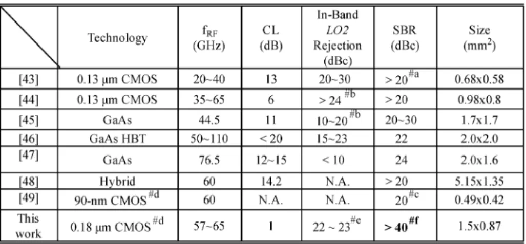
The results of the stand-alone SHM together with other state-of-the-art millimeter-wave mixers are summarized in Table I. It is found that the demonstrated silicon-based antipar-allel Schottky-diode SHM with no extra DC biasing circuit has a low LO power, good isolation performance and small size.
The measured conversion gain and power performance of the 60-GHz dual-conversion down-converter are depicted in Fig. 12. At , the conversion gain remains around 5 dB from 57 GHz to 66 GHz. The corresponding and
IIP3 are and 3 5 dBm, respectively. The
measured 3-dB bandwidth, shown in Fig. 13, is up to 2.1 GHz and the gain variation is less than 1 dB for frequency of up to 1.8 GHz. The measured noise figure at
keeps around 19 dB for frequencies from 100 MHz to 2.2 GHz. For a 60-GHz gigabit transmission, the bandwidth must be higher than 1 GHz for a 2-GHz RF channel. Here, the demonstrated dual-conversion down-converter has enough RF and IF bandwidths. Finally, the measured output IQ waveform
under is shown in Fig. 14. The phase and
TABLE I
COMPARISON OFMICROWAVE/MILLIMETER-WAVEMIXERS
Fig. 12. Measured conversion gain and power performance of the 60-GHz dual-conversion down-converter using 0.18- m CMOS technology.
Fig. 13. Measured conversion gain and noise figure of the 60-GHz dual-con-version down-converter using 0.18- m CMOS technology.
Fig. 14. Measured I/Q output waveform of the 60-GHz dual-conversion down-converter using 0.18- m CMOS technology.
IV. THEDEMONSTRATED60-GHz DUAL-CONVERSION UP-CONVERTER
The 60 GHz dual-conversion up-converter and its frequency planning are shown in Figs. 15(a) and 15(b), respectively. The frequency planning is similar to that of Fig. 5(b) for the compat-ibility with the frequency arrangement of generator in the 60 GHz dual-conversion down-converter. The signal is at 10 GHz when the frequency is also fixed at 10 GHz; thus, the sideband signal caused by the high-frequency conversion is 20 GHz away from the 60 GHz channel and easily filtered out by the subsequent bandpass circuits. However, leakage signal, located at 48 54 GHz, is very close to the 60-GHz signal. It is difficult to suppress the leakage signal by the subsequent bandpass circuits, meaning that leakage sig-nals could be emitted together with the desired 60-GHz signal. A good -to- isolation is very important in the transmitter design. Thus, an SHM using trifilar transformer is proposed to
Fig. 15. (a) Schematic and (b) frequency planning of the 60-GHz dual-conversion up-converter by using Schottky diodes in the 0.18- m CMOS technology.
solve the problem of port-to-port isolations. In addition, the 60 GHz up-converter consists of a single sideband (SSB) up-con-version mixer pumped by signal at low-frequency conver-sion and an differential driving amplifier inserted between the two-step up-conversion stages. Details of the schematics are presented below.
A. 60 GHz Sub-Harmonic Schottky-Diode Mixer Using Trifilar Transformer
The 60 GHz SHM includes a trifilar transformer for differ-ential and inputs, series-connected Schottky-diode APDPs in double-balanced configuration for sub-harmonic mixing, and a Marchand Balun for 60-GHz differential RF signal extraction. A trifilar transformer with one primary coil and two secondary coils is a useful microwave passive circuit [41] and has been employed in image-reject down-converters [42] and quadrature voltage-controlled oscillators. Here, we use a trifilar transformer with 2:1:1 turn ratios to implement an SHM in millimeter-wave frequency. The schematic and physical layout are illustrated in Fig. 16(a). The signal is fed via the center-taps of two secondary coils while the signal is coupled by the magnetic flux from the primary coil to two secondary coils. The design parameters are shown in Fig. 16(b)–16(d). The quality factor and inductance value of the primary/two secondary coils of the trifilar (at 25 GHz) are 11.8/8.5 and 1.2 nH/0.45 nH, respectively. The self-resonances are all around 48 GHz, and the coupling factor from primary to secondary coils ( and ) at 25 GHz is 0.51. The simulated
transmission coefficients in the cases of excitation are shown in Fig. 16(e), (f).
Due to the port arrangements, the mutual isolations between the LO and IF ports are achieved by the trifilar. As shown in Fig. 15(a), two series-connected APDPs are placed at the re-maining ports of a trifilar transformer such that the middle point of each series-connected APDPs is a virtual ground for the dif-ferential signal. Thus, an inherently good -to- iso-lation can be attained because differential RF signals are taken from the virtual-ground points. At the same time, -to-isolations are achieved due to the APDP configuration. In order to drive the external single-ended amplifier, a Marchand balun is used for the differential-to-single conversion. The Marchand balun adopts slotted shielding to block the lossy silicon substrate for loss reduction and to reduce the speed of the propagating wave for size reduction. Because the frequency between and RF signals is widely separated, the IF-to-RF isolation can be achieved by the bandpass response of the Marchand balun.
There is a trade-off in the coupling design for the and inputs to the ports connected to the APDPs because the tri-filar transformer deals with two signals with different frequen-cies at the same time. All the terminals are labeled as shown in Fig. 16(a). If the coupling between the ports (terminals of 1 and ) and the ports connected to the APDP (terminals of 2, , 3 and ) is too high, the signal transmitted from ports to the ports connected to the APDP increases; thus, the required power is lowered at the cost of low transmission between IF (terminals of 4 and ) and the ports connected to the
Fig. 16. (a) The trifilar schematic, (b), (c) quality factors and inductance values of the primary/two secondary cores, (d) coupling factor between primary and two secondary coils, and (e), (f) the simulated transmission coefficients in the cases of excitation.
APDP (terminals of 2, , 3 and ). Figs. 16(e) and 16(f) show the -to- and -to- insertion loss versus operating frequency by EM-simulations. A trade-off between the pumping power and the up-conversion loss exists in designing the coupling strength of a trifilar. In this work, the -to-insertion loss at 10 GHz is about 4.7 dB while the -to-insertion loss at 23.5 28 GHz is around 7 dB. The simple anal-ysis by hand calculation is described in Appendix A.
B. 10 GHz Single Sideband Gilbert Mixer and Differential Driving Amplifier
The 10-GHz SSB mixer consists of two Gilbert multipliers, a quadrature generator and two center-tapped inductors. Each multiplier is composed of a double-balanced Gilbert cell (
or ), input trans-conductance stage (
Fig. 17. Die photograph of the 60-GHz dual-conversion up-converter using 0.18- m CMOS technology.
or ), and one current source. It is difficult to generate a millimeter-wave transmitting signal with good side-band rejection by a direct up-conversion because the parasitic effects degrade the amplitude and phase accuracy of IQ signals. A dual conversion remedies the problem. The SSB mixer is used to up-convert the spectrum of the desired based-band IQ signal to the frequency with good sideband rejection at low-fre-quency conversion. The signal at frequency is then up-con-verted to 60 GHz by an SHM. Because the high-frequency mixer does not have sideband rejection, the frequency is set at 10 GHz to enable the undesired sideband signal generated by the high-frequency conversion to be easily filtered out by the subsequent external bandpass filter and power amplifier. Thus, generating a millimeter-wave signal with good sideband rejec-tion is achieved by a two-step conversion. In order to over-come headroom limitation, the T-coil inductors ( and ) are used as the output load for gain enhancement at
.
The differential driving amplifier, employed between the SHM and the sideband-rejection mixer, raises the output power before the signal enters the 60-GHz SHM. Because the frequency response of a cascode configuration is better than that of a common-source configuration, a higher maximum available gain (MAG) at 10 GHz can be obtained by the former under the same DC current. Here, the size of each transistor
is m . The fully-differential
architecture with symmetrical layout has less sensitivity to the parasitic effects at the ac-ground point. A differential trans-former is used at the output load to increase the dynamic range, and also to achieve conjugate impedance match to the SHM’s input via a turn ratio of 1.5.
C. Experimental Results
The die photo of the 60 GHz dual-conversion up-converter is shown in Fig. 17. The circuit area, excluding pads and test-key,
is mm , and the compact 60-GHz SHM with the
compact trifilar transformer occupies a mere mm . The differential baseband IQ signals are generated by applying the differential signals to a two-stage polyphase shifter to fa-cilitate the measurement. The is designed at 1 GHz for a 2-GHz channel. If the IQ generator is also deducted, the area of the SHM, amplifier, SSB mixer, and gener-ator, is mm (as marked by the white dashed line).
Fig. 18. Measured and simulated output reflection coefficient of the 60-GHz dual-conversion up-converter using 0.18- m CMOS technology.
Fig. 19. 60-GHz RF output power verses baseband input power for the different RF frequencies.
The total power consumption of the main circuit is 26 mA at a supply voltage of 2.5 V. Here, the driving amplifier con-sumes most of the DC power.
Fig. 18 shows the measured and simulated S-parameter of RF output reflection coefficient. The measured RF output return below 10 dB is from 50 to 66 GHz. Fig. 19 shows the mea-sured power performance. The for each channel is close
to and the maximum saturated power is 16
dBm at . Each 60-GHz channel has an almost
identical power performance. Moreover, the measured 51 66 GHz conversion gain, shown in Fig. 20, is around 2 dB and the RF bandwidth is basically limited by the output reflection coef-ficient of the RF marchand balun. Within the 3-dB bandwidth, the measured remains around 6 dBm in most cases.
Fig. 21 shows the measured SSB output power spectrum at
and , and the sideband
rejection (SBR) reaches 41.43 dB. The SBR is better than 40 dB over 50 66 GHz and remains nearly constant. The best
performance is nearly 44 dB rejection at ,
meaning that the quadrature signal keeps the amplitude and phase errors smaller that 0.2 dB and 1 , respectively. Moreover,
the (10-GHz signal leaked to the
in-terest band) suppression, referring to desired output power, is
Fig. 20. Measured conversion gain of the 60-GHz dual-conversion up-con-verter using standard 0.18- m CMOS technology.
Fig. 21. Sideband rejection ratio (SBR) of the 0.18- m CMOS 60-GHz dual-conversion up-converter at .
Fig. 22. Measured isolations and sideband rejection of the 60-GHz dual-con-version up-converter verses operating frequency.
about 22 23 dBc. The measured suppression and isolations across the entire 60 GHz bandwidth are shown in Fig. 22. Here,
-to- isolation is about 30 40 dB, and -to-isolation is better than 65 dB thanks to the fully-symmetrical design of the double-balanced SHM by using the trifilar trans-former and the APDPs structure.
TABLE II
COMPARISON OFSINGLE-SIDEBANDREJECTION OFMICROWAVE/MILLIMETER-WAVEUP-CONVERTERS
#a only from 27 GHz to 30 GHz #b Suppression (SHM)
#c SSB is achieved by using polyphase filter at 60 GHz #d Dual-conversion up-converter
#e suppression (DUC)
#f This performance almost remains the same over whole interesting 60 GHz bandwidth. The performances of the 60-GHz up-converter and other
state-of-the art up-converters at millimeter-wave frequency are summarized in Table II. Our proposed dual-conversion up-converter has the highest SBR over the 60 GHz bandwidth of any circuit on the list.
V. CONCLUSION
The introduction of Schottky diodes with a cut-off fre-quency of several hundred GHz in standard CMOS process has changed the scenario of the scaling rule. This en-abling technology makes possible the implementation of 60-GHz dual-conversion up-/down-converters using 0.18- m foundry CMOS process even though MOS transistors have
only of 50-GHz/60-GHz. Additionally, both
mi-crowave/millimeter-wave and analog design approaches are used to accomplish the low-cost 60-GHz transceiver. In the dual-conversion architecture, 60 GHz Schottky-diode SHMs are employed in the high-frequency conversion while analog mixers with accurate IQ signal generation are chosen for low-frequency conversion. Because the silicon-based Schottky diode possesses a low turn-on voltage and the advanced passive circuits, such as the proposed phase-inverter rat-race coupler and trifilar transformer, are available, the Schottky-diode mil-limeter-wave mixers using 0.18- m foundry CMOS process become practical. The demonstrated 60-GHz dual-conversion down-converter, operating from 57 66 GHz, has conversion
gain of 5 dB, of 5 dBm and of 5 dBm. The
corresponding Schottky-diode SHM requires only the small power of 1 dBm. For the 60-GHz dual-conversion up-con-verter, conversion gain of 2 dB, of 17 dBm, and broadband sideband rejection better than 40-dB are achieved. Based on the results of this work, incorporating the demon-strated 0.18- m CMOS dual-conversion up-/down-converters with high-performance HEMT-based LNA and PA gives an alternative attractive solution for 60-GHz transmission.
APPENDIXA
ANALYSIS FOR ATRIFILARWITHDIFFERENTEXCITATIONS The simple equivalent model of the trifilar with turn ratio of 2:1:1 is shown in Fig. 23. is magnetic coupling factor, and n is
equal to . and represent the
mag-netizing and leakage inductances of the primary coil, respec-tively. The simulated mutual coupling among two secondary coils is around 0.1, much smaller than that between primary and secondary coils, and thus is ignored here. Two impedances of reflected from port 2 and port 3 are in parallel with the shunt inductance , as illustrated in Fig. 23(b). In
this work, . and are the
self-induc-tance and parasitic resisself-induc-tance of primary (secondary) winding, respectively.
The voltage transformation in consideration of the leakage inductance effect and parasitic resistance is as follows:
(A.1) where the relation between and is defined as follow,
Fig. 23. (a) The diagram of the trifilar excited by a differential LO1 signal and (b) a simple equivalent model of the trifilar.
We can get the deviation of by (A.1) and (A.2)
(A.3) and the reflected coefficient of is expressed as follows:
(A.4)
where . The calculated is around 6.5 dB at 25
GHz according to the simulated parameters of the trifilar (
nH, nH, , ,
and at ). The simple analysis is close
to the simulated loss value of 7 dB in Fig. 16(e).
When the trifilar is excited by a differential IF signal from the two center-tape ports, the LO port illustrated in Fig. 24(a) is the virtual ground for the IF signal. Fig. 24(b) shows the simple equivalent model of the trifilar for estimating transmission coefficient. The magnetizing inductance of is shorted due to the virtual ground of the primary coil as shown in Fig. 24(b),
Fig. 24. (a) The diagram of the trifilar excited by a differential signal and (b) the simple equivalent model.
and only leakage inductance of and parasitic resis-tance are considered in the voltage transformation between the IF input and output ports.
The voltage transformation between IF input (port of ) and two output ports (ports of 23 and ) can be obtained by the voltage-division rule
(A.5)
where . Here, the reflected
coeffi-cient of is as follows:
(A.6)
and the deviation of is similar as the case of LO excitation by
applying (A.5) and (A.6) to (A.3). At ,
nH, , and is 1.54. By the hand
calculation, we can obtain dB at 10 GHz, similar to the simulated loss value of 4.7 dB in Fig. 16(f).
ACKNOWLEDGMENT
The authors would like to thank the National Chip Implemen-tation Center (CIC), Hsinchu, Taiwan, for chip fabrication, and National Nano Device Laboratory (NDL), Hsinchu, Taiwan, for measurement support.
REFERENCES
[1] C. H. Doan, S. Emami, A. M. Niknejad, and R. W. Brodersen, “Mil-limeter-wave CMOS design,” IEEE J. Solid-State Circuits, vol. 40, no. 1, pp. 144–155, Jan. 2005.
[2] S. Reynolds, B. Floyd, U. Pfeiffer, and T. Zwick, “60 GHz transceiver circuits in SiGe bipolar technology,” in Proc. IEEE ISSCC Dig. Tech.
Papers, Feb. 2004, pp. 442–538.
[3] B. Razavi, “A 60 GHz direct-conversion CMOS receiver,” in Proc.
IEEE ISSCC Dig. Tech. Papers, Feb. 2005, pp. 400–606.
[4] S. K. Reynolds, B. A. Floyd, U. R. Pfeiffer, T. Beukema, J. Grzyb, C. Haymes, B. Gaucher, and M. Soyuer, “A silicon 60-GHz receiver and transmitter chipset for broadband communications,” IEEE J.
Solid-State Circuits, vol. 41, no. 12, pp. 2820–2831, Dec. 2006.
[5] M. Tanomura, Y. Hamada, S. Kishimoto, M. Ito, N. Orihashi, K. Maruhashi, and H. Shimawaki, “TX and RX frond-ends for 60 GHz band in 90 nm standard bulk CMOS,” in Proc. IEEE ISSCC Dig. Tech.
Papers, Feb. 2008, pp. 558–635.
[6] B. Razavi, “A millimeter-wave CMOS heterodyne receiver with on-chip LO and divider,” IEEE J. Solid-State Circuits, vol. 43, no. 2, pp. 477–485, Feb. 2008.
[7] E. Cohen, C. G. Jakobson, S. Ravid, and D. Ritter, “A bidirestional TX/RX four-element phase array at 60 GHz with RF-IF conversion block in 90-nm CMOS process,” IEEE Trans. Microw. Theory Tech., vol. 58, no. 5, pp. 1438–1446, May 2010.
[8] J. J. Kuo, Z. M. Tsai, K. Y. Lin, and H. Wang, “Design and analysis of novel linearization technique of cascode cell in a 60-GHz CMOS demodulator,” IEEE Trans. Microw. Theory Tech., vol. 59, no. 2, pp. 456–465, Feb. 2011.
[9] P. Pursula, T. Karttaavi, M. Kantanen, A. Lamminen, J. Holmberg, M. Lahdes, I. Marttila, A. Luukanen, and T. Vähä-Heikkilä, “60-GHz millimeter-wave identification reader on 90-nm CMOS and LTCC,”
IEEE Trans. Microw. Theory Tech., vol. 59, no. 4, pp. 1166–1173, Apr.
2011.
[10] D. Dawn, P. Sen, S. Sarker, B. Perumana, S. Pinel, and J. Lasker, “60-GHz integrated transmitter development in 90-nm CMOS,”
IEEE J. Solid-State Circuits, vol. 57, no. 10, pp. 2354–2367,
Oct. 2009.
[11] C. Marcu, D. Chowdhury, C. Thakkar, L. K. Kong, M. Tabesh, J. D. Park, W. Yanjie, B. Afshar, A. Gupta, A. Arbabian, S. Gambini, R. Zamani, A. M. Niknejad, and E. Alon, “A 90 nm CMOS low-power 60 GHz transceiver with integrated baseband circuitry,” IEEE J.
Solid-State Circuits, vol. 44, no. 12, pp. 3434–3447, Dec. 2009.
[12] J. Lee, Y. Chen, and H. Yenlin, “A low-power low-cost fully-inte-grated 60-GHz transceiver system with OOK modulation and on-board antenna assembly,” IEEE J. Solid-State Circuits, vol. 45, no. 2, pp. 264–275, Feb. 2010.
[13] E. Juntunen, M. C.-H. Leung, F. Barale, A. Rachamadugu, D. A. Yeh, B. G. Perumana, P. Sen, D. Dawn, S. Sarker, S. Pinel, and J. Lasker, “A 60-GHz 38-pJ/bit 3.5-Gb/s 90-nm CMOS OOK digital radio,” IEEE
Trans. Microw. Theory Tech., vol. 58, no. 2, pp. 348–355, Feb. 2010.
[14] M. Varonen, M. Karkkainen, M. Kantanen, and K. Halonen, “Mil-limeter-wave integrated circuits in 65-nm CMOS,” IEEE J. Solid-State
Circuits, vol. 43, no. 9, pp. 1991–2002, Sep. 2008.
[15] A. Tomkins, R. A. Aroca, T. Yamamoto, S. T. Nicolson, Y. Doi, and S. P. Voinigescu, “A zero-IF 60 GHz 65 nm CMOS transceiver with direct BPSK modulation demonstrating up to 6 Gb/s data rates over a 2-m wireless link,” IEEE J. Solid-State Circuits, vol. 57, no. 10, pp. 2085–2099, Oct. 2009.
[16] J. Borremans, K. Raczkowshi, and P. Wambacq, “A digitally controlled compact 57-to-66 GHz front-end in 45 nm digital CMOS,” in Proc.
IEEE ISSCC Dig. Tech. Papers, Feb. 2009, pp. 492–494.
[17] S. A. Mass, Microwave Mixers, 2nd ed. Norwood, MA: Artech House, 1993.
[18] C. Hutchinson, M. Frank, and K. Negus, “Silicon bipolar 12 GHz downconverter for satellite receivers,” in Proc. Bipolar/BiCMOS
Circuits and Technology Meeting Papers, 1995, pp. 198–201.
[19] V. Milanović, M. Gaitan, J. C. Marshall, and M. E. Zaghloul, “CMOS foundry implementation of Schottky diodes for RF detection,” IEEE J.
Solid-State Circuits, vol. 43, no. 12, pp. 2210–2214, Dec. 1996.
[20] S. Sankaran and K. K. O, “Schottky barrier diodes for millimeter-wave detection in a foundry CMOS process,” IEEE Electron Device Lett., vol. 26, no. 7, pp. 492–494, Jul. 2005.
[21] S. Sankaran and K. K. O. , “Schottky diode with cutoff frequency of 400 GHz fabricated in 0.18 m CMOS,” IEE Electron. Lett., vol. 41, no. 8, pp. 506–508, Apr. 2005.
[22] S. Sankaran and K. K. O., “A ultra-wideband amplitude modulation (AM) detector using Schottky barrier diodes fabricated in foundry CMOS technology,” IEEE J. Solid-State Circuits, vol. 42, no. 5, pp. 1058–1064, May 2007.
[23] D. Shim, S. Sankaran, and K. K. O, “Complementary antiparallel schottky barrier diode pair in a 0.13- m logic CMOS technology,”
IEEE Electron Device Lett., vol. 29, no. 6, pp. 606–608, Jun.
2008.
[24] U. R. Pfeiffer, C. Mishra, R. M. Rassel, S. Pinkett, and S. K. Reynolds, “Schottky barrier diode circuits in silicon for future millimeter-wave and terahertz applications,” IEEE Trans. Microw. Theory Tech, vol. 56, no. 2, Feb. 2008.
[25] C. Mao, C. S. Nallani, S. Sankaran, E. Seok, and K. K. O., “125-GHz diode frequency doubler in 0.13- m CMOS,” IEEE J. Solid-State
Cir-cuits, vol. 44, no. 5, May 2009.
[26] E. Seok, D. Shim, C. Mao, R. Han, S. Sankaran, C. Cao, W. Knap, and K. K. O. , “Progress and challenges toward Terahertz CMOS integrated circuits,” IEEE J. Solid-State Circuits, vol. 45, no. 8, Aug. 2010. [27] A. Fujihara, E. Mizuki, H. Miyamoto, Y. Makino, K. Yamanoguchi,
and N. Samoto, “High performance 60-GHz coplanar MMIC LNA using InP heterojunction FETs with AlAs/InAs superlattice layer,” in Proc. IEEE MTT-S Int. Microw. Symp. Dig., Jun. 7–12, 2000, pp. 21–24.
[28] C. F. Campbell, S. Moochalla, D. Daugherty, W. J. Taft, M. Y. Kao, and D. Fanning, “V band amplifier MMICs exhibiting low power slump characteristic utilizing a production released 0.15 um GaAs PHEMT process,” in Proc. IEEE MTT-S Int. Microw. Symp. Dig., Jun. 7–12, 2009, pp. 433–436.
[29] S. Emami, R. F. Wiser, E. Ali, M. G. Forbes, M. Q. Fordon, X. Guan, S. Lo, P. T. McElwee, J. Parker, J. R. Tani, J. M. Gilbert, and C. H. Doan, “A 60 GHz CMOS phase-array transceiver pair for multi-Gb/s wireless communications,” in Proc. IEEE ISSCC Dig. Tech. Papers, Feb. 2011, pp. 164–166.
[30] T. Wang and K. Wu, “Size-reduction and band-broadening design technique of uniplanar hybrid ring coupler using phase inverter for M(H)MIC’s,” IEEE Trans. Microw. Theory Tech., vol. 47, no. 2, pp. 198–206, Feb. 1999.
[31] C. Y. Chang and C. C. Yang, “A novel broadband Chebyshev-response rat-race ring coupler,” IEEE Trans. Microw. Theory Tech., vol. 47, no. 4, pp. 455–462, Apr. 1999.
[32] H. J. Wei, C. C. Meng, and S. W. Yu, “A Chebyshev-response step-impedance phase-inverter rat-race coupler directly on lossy silicon sub-strate and its Gilbert mixer application,” IEEE Trans. Microw. Theory
Tech., vol. 59, no. 4, pp. 882–893, Apr. 2011.
[33] H. J. Wei, C. C. Meng, C. H. Chang, and G. W. Huang, “A UWB Gilbert down-converter with lumped-distributed phase-inverter rat-race cou-pler based on Chebyshev band-broadening technique,” IEE Electron.
Lett., vol. 47, no. 15, pp. 859–861, Jul. 2011.
[34] J. W. Lee and S. M. Heo, “A 27 GHz, 14 dBm CMOS power amplifier using 0.18 m common-source MOSFETs,” IEEE Microw. Wireless
Compon. Lett., vol. 18, no. 11, pp. 755–757, Nov. 2008.
[35] Y. N. Jen, C. T. Peng, and T. W. Huang, “A 20 to 24 GHz 16.8 dBm fully integrated power amplifier using 0.18 m CMOS process,” IEEE Microw. Wireless Compon. Lett., vol. 19, no. 1, pp. 42–44, Jan. 2009.
[36] S. E. Gunnarsson, “Analysis and design of a novel 4 subharmonically pumped resistive HEMT mixer,” IEEE Trans. Microw. Theory Tech., vol. 56, no. 4, pp. 809–816, Apr. 2008.
[37] H. K. Chiou and T. Y. Yang, “Low-loss and broadband asymmetric broadside coupled balun for mixer design in 0.18- m CMOS tech-nology,” IEEE Trans. Microw. Theory Tech., vol. 56, no. 4, pp. 835–848, Apr. 2008.
[38] C. H. Lien, C. H. Wang, C. S. Lin, P. S. Wu, K. Y. Lin, and H. Wang, “Analysis and design of reduced-size marchand rat-race hybrid for mil-limeter-wave compact balanced mixers in 130-nm CMOS process,”
IEEE Trans. Microw. Theory Tech., vol. 57, no. 8, pp. 1966–1977, Aug.
2009.
[39] H. K. Chiou and J. Y. Lin, “Symmetric offset stack balun in standard 0.13- m CMOS technology for three broadband and low-loss bal-anced passive mixer design,” IEEE Trans. Microw. Theory Tech., vol. 59, no. 6, pp. 1529–1538, Jun. 2011.
[40] C. M. Lin, H. K. Lin, Y. A. Lai, C. P. Chang, and Y. H. Wang, “A 10–40 GHz broadband subharmonic monolithic mixer in 0.18 m CMOS technology,” IEEE Microw. Wireless Compon. Lett., vol. 19, no. 2, pp. 95–97, Feb. 2009.
[41] J. R. Long, “Monolithic transformers for silicon RF IC design,” IEEE
pp. 2075–2085, Oct. 2007.
[45] K. Hettak, G. A. Morin, and M. G. Stubbs, “A novel miniature multi-layer CPW single sideband CPW mixer for up conversion at 4.5 GHz,”
IEEE Microw. Wireless Compon. Lett., vol. 15, no. 9, pp. 606–608, Sep.
2005.
[46] H. Y. Chang, T. W. Huang, H. Wang, Y. C. Wang, P. C. Chao, and C. H. Chen, “Broad-band HBT BPSK and IQ modulator MMICs and millimeter-wave vector signal characterization,” IEEE Trans. Microw.
Theory Tech., vol. 52, no. 3, pp. 908–919, Mar. 2004.
[47] D. S. McPherson and S. Lucyszyn, “Vector modulator for W-band soft-ware radar techniques,” IEEE Trans. Microw. Theory Tech., vol. 49, no. 8, pp. 1451–1461, Aug. 2001.
[48] S. Kishimoto, K. Maruhashi, M. Ito, Y. Hamada, and K. Ohata, “60-GHz-band Intentional LO-leakage APDP mixer for SSB self-hetero-dyne transmitter module,” in Proc. IEEE MTT-S Int. Microw. Symp.
Dig., Jun. 6–11, 2006, pp. 183–186.
[49] P. Ali and B. Razavi, “A new transceiver architecture for the 60-GHz band,” IEEE J. Solid-State Circuits, vol. 44, no. 3, pp. 751–762, Mar. 2009.
[50] C. M. Lo, C. S. Lin, and H. Wang, “A miniature V-band 3-Stage cas-code LNA in 0.13 m CMOS,” in Proc. ISSCC Dig. Tech. Papers, Feb. 2006, pp. 322–323.
[51] S. Pellerano, Y. Palaskas, and K. Soumyanath, “A 64 GHz 6.5 dB NF 15.5 dB gain LNA in 90 nm CMOS,” in Proc. ESSCIRC, Sep. 2007, pp. 352–355.
[52] C. Weyers, P. Mayer, J. W. Kunze, and U. Langmann, “A 22.3 dB voltage gain 6.1 dB NF 60 GHz LNA in 65 nm CMOS with differential output,” in Proc. ISSCC Dig. Tech. Papers, Feb. 2008, pp. 192–193. [53] K. Maruhashi, K. Ohata, and M. Madihian, “A single-bias
diode-reg-ulated 60 GHz monolithic LNA,” in Proc. IEEE MTT-S Int. Microw.
Symp. Dig., Jun. 30–Jul. 3 1997, pp. 443–446.
[54] T. LaRocca and M. C. Frank Chang, “60 GHz CMOS differential and transformer-coupled power amplifier for compact design,” in Proc.
IEEE Radio Freq. Integr. Circuits Symp., Jun. 2008, pp. 65–68.
[55] C. Y. Law and A. V. Pham, “A high-gain 60 GHz power amplifier with 20 dBm output power in 90 nm CMOS,” in Proc. IEEE ISSCC
Dig. Tech. Papers, Feb. 2010, pp. 426–427.
[56] J. W. Lai and A. Valdes-Garcia, “A 1 V 17.9 dBm 60 GHz power am-plifier in standard 65 nm CMOS,” in Proc. IEEE ISSCC Dig. Tech.
Papers, Feb. 2010, pp. 424–425.
[57] J. Chen and A. M. Niknejad, “A compact 1 V 18.6 dBm 60 GHz power amplifier in 65 nm CMOS,” in Proc. IEEE ISSCC Dig. Tech. Papers, Feb. 2011, pp. 432–433.
[58] M. Abbasi, T. Kjellberg, A. de Graauw, E. van der Heijden, R. Roovers, and H. Zirath, “A broadband differential cascode power amplifier in 45 nm CMOS for high-speed 60 GHz system-on-chip,” in Proc. IEEE
Radio Freq. Integr. Circuits Symp., Jun. 2010, pp. 533–536.
Chinchun Meng received the B.S. degree in
elec-trical engineering from National Taiwan University, Taipei, Taiwan, in 1985 and the Ph.D. degree in elec-trical engineering from University of California, Los Angeles, in 1992.
He is currently a Full Professor in the Department of Electrical Engineering at National Chiao Tung University, HsinChu, Taiwan. His current research interests are in the areas of radio frequency integrated circuits, microwave and millimeter-wave integrated circuits.
Ta-Wei Wang was born in Changhua, Taiwan, in
1985. He received the B.S. degree in Department of Communication Engineering from National Chiao Tung University, Hsinchu, Taiwan, in 2007, and the M.S. degree in Institute of Communications Engineering from National Chiao Tung University, Hsinchu, Taiwan, in 2009.
He worked on CMOS, SiGe BiCMOS and pHEMT microwave and millimeter wave integrated circuits for his master work.
Tai-Lin Lo was born in Tainan, Taiwan, in 1985. He
received the B.S. degree in Department of Electrical Engineering, National Chung Cheng University, Chiayi, Taiwan, in 2007, and the M.S. degree in the Department of Communication Engineering from Nation Chiao Tung University, Hsinchu, Taiwan, in 2009.
He worked on CMOS, SiGe BiCMOS and pHEMT microwave and millimeter wave integrated circuits for his master work.
Chia-Ling Wang was born in Tainan, Taiwan, in
1986. She received the B.S. degree in Department of Communication Engineering from National Chiao Tung University, Hsinchu, Taiwan, in 2008, and the M.S. degree in Institute of Communications Engineering from National Chiao Tung University, Hsinchu, Taiwan, in 2010.
Her current research focuses on the CMOS Radio Frequency Integrated Circuit (RFIC) circuit design.