Continuous wave operation of current injected GaN vertical cavity surface emitting
lasers at room temperature
Tien-Chang Lu, Shih-Wei Chen, Tzeng-Tsong Wu, Po-Min Tu, Chien-Kang Chen, Cheng-Hung Chen, Zhen-Yu Li, Hao-Chung Kuo, and Shing-Chung Wang
Citation: Applied Physics Letters 97, 071114 (2010); doi: 10.1063/1.3483133 View online: http://dx.doi.org/10.1063/1.3483133
View Table of Contents: http://scitation.aip.org/content/aip/journal/apl/97/7?ver=pdfcov
Published by the AIP Publishing
Articles you may be interested in
An improved active region concept for highly efficient GaSb-based optically in-well pumped vertical-external-cavity surface-emitting lasers
Appl. Phys. Lett. 93, 181113 (2008); 10.1063/1.3013311
Fabrication and performance of blue GaN-based vertical-cavity surface emitting laser employing AlN GaN and Ta 2 O 5 SiO 2 distributed Bragg reflector
Appl. Phys. Lett. 87, 081105 (2005); 10.1063/1.2032598
Over 3 W high-efficiency vertical-external-cavity surface-emitting lasers and application as efficient fiber laser pump sources
Appl. Phys. Lett. 86, 211116 (2005); 10.1063/1.1935756
Low-threshold lasing of InGaN vertical-cavity surface-emitting lasers with dielectric distributed Bragg reflectors
Appl. Phys. Lett. 83, 830 (2003); 10.1063/1.1596728
Minimum temperature sensitivity of 1.55 m vertical-cavity lasers at 30 nm gain offset
Appl. Phys. Lett. 72, 1814 (1998); 10.1063/1.121318
This article is copyrighted as indicated in the article. Reuse of AIP content is subject to the terms at: http://scitation.aip.org/termsconditions. Downloaded to IP: 140.113.38.11 On: Wed, 30 Apr 2014 10:03:49
Continuous wave operation of current injected GaN vertical cavity surface
emitting lasers at room temperature
Tien-Chang Lu,a兲 Shih-Wei Chen, Tzeng-Tsong Wu, Po-Min Tu, Chien-Kang Chen, Cheng-Hung Chen, Zhen-Yu Li, Hao-Chung Kuo,a兲 and Shing-Chung Wanga兲
Department of Photonics and Institute of Electro-Optical Engineering, National Chiao-Tung University, 1001 Ta Hsueh Rd., Hsinchu 300, Taiwan
共Received 2 July 2010; accepted 4 August 2010; published online 18 August 2010兲
We report the demonstration of the continuous wave laser action on GaN-based vertical cavity surface emitting lasers at room temperature. The laser structure consists of a ten-pair Ta2O5/SiO2
distributed Bragg reflector 共DBR兲, a 7-thick optical cavity, ten-pairs InGaN/GaN multiquantum wells with an AlGaN electron blocking layer, and a 29-pair AlN/GaN DBR. The laser has a threshold current of about 9.7 mA corresponding to the current density of about 12.4 kA/cm2and
a turn-on voltage about 4.3 V at 300 K. The lasing wavelength was 412 nm with a linewidth of about 0.5 nm. A spontaneous emission coupling efficiency factor of about 5⫻10−3 and the degree of
polarization of about 55% were measured, respectively. The laser beam has a narrow divergence angle of about 8°. © 2010 American Institute of Physics.关doi:10.1063/1.3483133兴
GaN-based materials have attracted a great attention since the early 1990s due to the wide direct band gap and the promising potential for the optoelectronic devices such as light emitting diodes and laser diodes.1,2 So far, GaN-based edge emitting lasers have been demonstrated and applied in commercial products for high density optical storage appli-cations. However, the vertical cavity surface emitting lasers 共VCSELs兲, with superior characteristics such as the single longitudinal mode emission, low divergence angle, and array capability, are still under development and currently gaining much attention. Optically pumped GaN-based VCSELs have been reported by using different kinds of optical cavity struc-tures, such as dielectric distributed Bragg reflectors 共DBR兲 VCSELs with cavities consisting of dielectric top and bottom DBRs,3and hybrid DBR VCSELs with cavities consisting of epitaxially grown nitride bottom DBRs and dielectric top DBRs.4We have recently demonstrated the continuous wave 共cw兲 current injection of GaN-based VCSEL with hybrid mirrors at 77 K in 2008.5 Subsequently, the room tempera-ture operation of GaN-based VCSEL devices was reported using optical cavities sandwiched by double dielectric DBRs.6,7 The major improvements of their devices to achieve room temperature operation are by using a thinner transparent conducting layer of about 50 nm to reduce the internal optical loss and by using the GaN substrate to ensure the good crystal quality of active layers. However, to form VCSELs with double dielectric DBRs required complex fab-rication process, such as laser lift-off or elaborated polishing and bonding process.8 In this paper, we report the achieve-ment of cw room temperature lasing with hybrid DBR cavity and a thin indium-tin-oxide 共ITO兲 layer of 30 nm as the transparent conducting layer combining with a thin heavily doped p-type InGaN contact layer to reduce the optical loss while maintaining good current spreading capability. More-over, we inserted an AlGaN electric blocking layer on the top of the InGaN multiple quantum well共MQW兲 to prevent the carrier overflow.9The lasing characteristics such as laser
out-put power and device voltage versus injected current charac-teristics, degree of polarization共DOP兲, divergence angle, and spontaneous emission coupling factor have been measured and investigated.
Figure 1共a兲 shows the schematic diagram of the whole GaN-based VCSEL structure. In the structure, the positions of the ITO layer and MQWs region are located at the node
a兲Electronic addresses: [email protected],
[email protected], and [email protected].
FIG. 1.共Color online兲 共a兲 The schematic diagram of the overall GaN-based VCSEL structure with hybrid mirrors. 共b兲 The CCD image of GaN-based VCSEL devices operated under 2 mA at room temperature.
APPLIED PHYSICS LETTERS 97, 071114共2010兲
0003-6951/2010/97共7兲/071114/3/$30.00 97, 071114-1 © 2010 American Institute of Physics
This article is copyrighted as indicated in the article. Reuse of AIP content is subject to the terms at: http://scitation.aip.org/termsconditions. Downloaded to IP: 140.113.38.11 On: Wed, 30 Apr 2014 10:03:49
and antinode positions of the electric field, respectively, to reduce the absorption from the ITO layer and to further increase the coupling between the electric field and MQWs region. The VCSEL structure was grown on a 2 in. sapphire substrate by the metal-organic chemical vapor deposition system. The substrate was thermally cleaned in the hydrogen ambient for 5 min at 1100 ° C, and then a 30 nm thick GaN nucleation layer was grown at 500 ° C. The growth tempera-ture was raised up to 1100 ° C for the growth of a 2 m thick GaN buffer layer. The subsequent epitaxial structure consisted of a 29-pair AlN/GaN DBR, a 7 cavity 共 = 410 nm兲 including a 860 nm thick n-GaN layer, ten-pairs InGaN/GaN共2.5 nm/12.5 nm兲 MQWs, a 24 nm thick AlGaN layer as the electron blocking layer, a 110 nm thick p-GaN layer, and a 2 nm thick p+ InGaN layer as the contact layer.
The AlGaN electron blocking layer was served to reduce the electron overflow to the p-GaN layer. In order to reduce the crack problems encountered in the AlN/GaN DBRs, we in-serted one AlN/GaN superlattice into each five DBR periods at first 20 pairs of DBR. Then the superlattice was inserted into each three DBR periods for the remaining nine pairs of DBR to reduce the tensile strain.10In the fabrication process, a 200 nm thick SiNxlayer was deposited by the plasma
en-hanced chemical vapor deposition as a current confined layer. By this way, the current injection aperture of VCSEL devices was about 10 m in diameter. Then, a 30 nm thick ITO layer was deposited as the current spreading layer due to the poor conductivity of the p-GaN layer and annealed at 600 ° C for 10 min by rapid thermal annealing. The 2 nm thick p+ InGaN layer on the p-GaN surface can further
re-duce the series resistance between the thin ITO layer and the p-GaN layer with a slight increase of absorption. Then, the p-contact and n-contact were deposited with Ni/Au of about 20 nm/150 nm and Ti/Al/Ni/Au of about 20 nm/150 nm/20 nm/150 nm by the e-gun system, respectively. Finally, ten-pairs Ta2O5/SiO2 of the top dielectric DBR were deposited
by the ion-assisted e-gun system to complete the whole GaN-based VCSEL devices. Both of the 29-pair AlN/GaN DBR and the ten-pair Ta2O5DBR show a high reflectivity of over
99% at the peak wavelength at 410 nm in the n-k measure-ment system. Figure 1共b兲 shows the charge-coupled device 共CCD兲 image of a VCSEL device injected at 2 mA under cw current injection at room temperature.
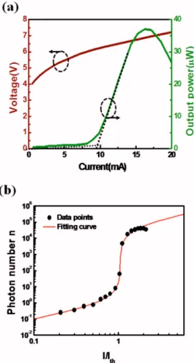
The GaN-based VCSEL devices with current injection apertures of about 10 m in diameter were tested by using a Keithely 238 cw current source. The emission light was col-lected by a 100 m diameter multimode fiber and fed into the spectrometer using a grating of 1800 g/mm with a tral resolution of about 0.15 nm. The output from the spec-trometer was detected by a CCD to record the emission spectrum. The VCSEL devices were then measured at envi-ronment temperature at 300 K. Figure 2共a兲 shows L-I-V curves at 300 K. The dashed line is the linear fitting curve of the laser output power versus injection current. A clear lasing transition from spontaneous emission to stimulated emission can be observed at room temperature. From the linear fitting curve, the laser threshold current is around 9.7 mA corre-sponding to the current density of about 12.4 kA/cm2. The
relative low threshold at room temperature operation could be due in part to the prevention of carrier overflow by using the electron blocking layer on top of the MQWs and the lower internal absorption loss of the thinner ITO layer. The
turn-on voltage is about 4.3 V indicating the good electrical contact of the 30 nm ITO transparent layer and the 2 nm thick InGaN layers. The output laser intensity from the sample increased linearly with current injection beyond the threshold current. However, the laser intensity started to roll over at higher injection current beyond 15 mA due to the thermal effect. We estimated the spontaneous emission cou-pling factor from the log-log plot of L-I curve as shown in Fig.2共b兲. The data points are matched well to the solid fitting line calculated from microcavity laser rate equations.11From the curve, we obtained an estimated  value of about 5 ⫻10−3.
Figure 3共a兲 shows the emission spectra of our GaN-based VCSEL devices at current injection of 0.6Ith, 1Ith, and
1.2Ith, respectively. The laser emission wavelength was mea-sured to be 412 nm with a linewidth of about 0.5 nm. The inset of Fig.3共b兲shows the CCD image of a lasing spot size of about 2 m in diameter. Finally, using the angular-resolved measurement system, the laser intensity at different angles emitted from the GaN-based VCSELs was collected by using a 600 m fiber. Figure 3共b兲 shows the measure-ment data at different angles and the solid curve is the fitting curve. We obtained a laser beam divergence angle of about 8°. Figure 3共c兲shows the DOP of the laser beam. The solid line is the fitting curve. The DOP value was estimated to be about 55°.
FIG. 2.共Color online兲 共a兲 The output power and the voltage as a function of injection current at 300 K. The threshold current and turn-on voltage are about 9.7 mA and 4.3 V.共b兲 The laser emission intensity vs injection current in logarithmic scale. The circle points and the solid curve are the measure-ment data and the fitting curve. Thevalue is about 5⫻10−3.
071114-2 Lu et al. Appl. Phys. Lett. 97, 071114共2010兲
This article is copyrighted as indicated in the article. Reuse of AIP content is subject to the terms at: http://scitation.aip.org/termsconditions. Downloaded to IP: 140.113.38.11 On: Wed, 30 Apr 2014 10:03:49
In summary, we have demonstrated the cw room tem-perature operation of GaN-based VCSELs with hybrid mir-rors. The laser has a thin ITO layer of 30 nm as the trans-parent conducting layer combining with a thin heavily doped p-type InGaN contact layer to reduce the optical loss while maintaining good current spreading capability. An AlGaN electric blocking layer on the top of the InGaN MQWs is also inserted to prevent the carrier overflow. At 300 K, the laser has a threshold current at 9.7 mA corresponding to 12.4 kA/cm2. The laser emission wavelength is 412 nm with a linewidth of about 0.5 nm. The laser has an estimated spontaneous emission coupling factor of about 5⫻10−3. The
DOP and divergence angle of the laser are measured to be 55% and 8°, respectively.
The authors would like to thank the Canon Co. for their technical support of ITO deposition. The study was sup-ported by the MOE ATU Program, Nano Facility Center and, in part, by the National Science Council in Taiwan under Contract Nos. NSC98-3114-E009-002-002, NSC98-3114-M-009-001, and NSC98-2923-E-009-001-MY3.
1S. Nakamura, M. Senoh, S. Nagahama, N. Iwasa, T. Yamada, T. Mat-sushita, Y. Sugimoto, and H. Kiyoku,Appl. Phys. Lett. 70, 868共1997兲.
2S. Nakamura,Science 281, 956共1998兲.
3Y.-K. Song, H. Zhou, M. Diagne, I. Ozden, A. Vertikov, A. V. Nurmikko, C. Carter-Coman, R. S. Kern, F. A. Kish, and M. R. Krames,Appl. Phys. Lett. 74, 3441共1999兲.
4T. Someya, K. Tachibana, J. Lee, T. Kamiya, and Y. Arakawa, Jpn. J.
Appl. Phys., Part 2 37, L1424共1998兲.
5T. C. Lu, C. C. Kao, H. C. Kuo, G. S. Huang, and S. C. Wang,Appl. Phys.
Lett. 92, 141102共2008兲.
6Y. Higuchi, K. Omae, H. Matsumura, and T. Mukai,Appl. Phys. Express
1, 121102共2008兲.
7K. Omae, Y. Higuchi, K. Nakagawa, H. Matsumura, and T. Mukai,Appl.
Phys. Express 2, 052101共2009兲.
8S. C. Wang, T. C. Lu, C. C. Kao, J. T. Chu, G. S. Huang, H. C. Kuo, S. W. Chen, T. T. Kao, J. R. Chen, and L. F. Lin,Jpn. J. Appl. Phys., Part 1 46,
5397共2007兲.
9J. R. Chen, C. H. Lee, T. S. Ko, Y. A. Chang, T. C. Lu, H. C. Kuo, Y. K. Kuo, and S. C. Wang,J. Lightwave Technol. 26, 329共2008兲.
10G. S. Huang, T. C. Lu, H. H. Yao, H. C. Kuo, S. C. Wang, C. W. Lin, and L. Chang,Appl. Phys. Lett. 88, 061904共2006兲.
11G. Bjork and Y. Yamamoto,IEEE J. Quantum Electron. 27, 2386共1991兲. FIG. 3. 共Color online兲 共a兲 The emis-sion spectra were recorded at injection current of 0.6Ith, 1Ith, and 1.2Ith. 共b兲 The laser divergence angle of about 8° was measured by the angular-resolved measurement system. The inset image shows the lasing spot with the diam-eter of about 2 m.共c兲 The DOP of VCSEL device is about 55%. The circle points are the measurement re-sults and the solid line is the fitting curve.
071114-3 Lu et al. Appl. Phys. Lett. 97, 071114共2010兲
This article is copyrighted as indicated in the article. Reuse of AIP content is subject to the terms at: http://scitation.aip.org/termsconditions. Downloaded to IP: 140.113.38.11 On: Wed, 30 Apr 2014 10:03:49