IEEE ELECTRON DEVICE LETTERS, VOL. 34, NO. 3, MARCH 2013 399
Characteristics and Mechanisms of
Silicon-Oxide-Based Resistance
Random Access Memory
Kuan-Chang Chang, Tsung-Ming Tsai, Ting-Chang Chang, Senior Member, IEEE, Hsing-Hua Wu, Jung-Hui Chen,
Yong-En Syu, Geng-Wei Chang, Tian-Jian Chu, Guan-Ru Liu, Yu-Ting Su, Min-Chen Chen, Jhih-Hong Pan,
Jian-Yu Chen, Cheng-Wei Tung, Hui-Chun Huang, Ya-Hsiang Tai, Der-Shin Gan, and Simon M. Sze
Abstract—Traditionally, a large number of silicon oxide mate-rials are extensively used as various dielectrics for semiconductor industries. In general, silicon oxide cannot be used as resistance random access memory (RRAM) due to its insulating electrical properties. In this letter, we have successfully produced resistive switching and forming-free behaviors by zinc doped into silicon oxide. The current–voltage fitting data show that current trans-port mechanism is governed by Poole–Frenkel behavior in high-resistance state and Ohm’s law in low-high-resistance state, consisting with filament theory. Additionally, good endurance and retention reliabilities are exhibited in the zinc-doped silicon oxide RRAM.
Index Terms—Filament, resistive switch, silicon oxide, Zn.
I. INTRODUCTION
R
ECENTLY, modern semiconductor nonvolatile memories (NVMs) have been scaled constantly to achieve large ca-pacity while device features approach the sub-100-nm regime to store a large amount of information. Nevertheless, for conven-tional charge-storage-based memories [1]–[4], the increasing demand for device densities by scaling dimension is expected to be a major challenge due to the technical and physical limitations. Resistance random access memory (RRAM) is one of the promising candidates for next-generation NVMs, due to its simple cell structure, low operating voltage, high operating speed, and nondestructive readout [5]–[10].Manuscript received December 11, 2012; revised December 24, 2012; accepted December 29, 2012 Date of publication February 14, 2013; date of current version February 20, 2013. This work was supported by the National Science Council of the Republic of China under Contracts NSC-101-2120-M-110-002 and NSC 101-2221-E-110-044-MY3. The review of this letter was arranged by Editor M. Jurczak.
K.-C. Chang, T.-M. Tsai, T.-J. Chu, J.-H. Pan, C.-W. Tung, H.-C. Huang, and D.-S. Gan are with the Department of Materials and Optoelectronic Science, National Sun Yat-Sen University, Kaohsiung 804, Taiwan.
T.-C. Chang, Y.-E. Syu, G.-R. Liu, Y.-T. Su, M.-C. Chen, and J.-Y. Chen are with the Department of Physics, National Sun Yat-Sen University, Kaohsiung 804, Taiwan, and also with the Advanced Optoelectronics Technology Center, National Cheng Kung University, Tainan 701, Taiwan (e-mail: tcchang@mail. phys.nsysu.edu.tw).
H.-H. Wu, G.-W. Chang, and Y.-H. Tai are with the Department of Photonics and the Institute of Electro-Optical Engineering, National Chiao Tung Univer-sity, Hsinchu 300, Taiwan.
J.-H. Chen is with the Department of Chemistry, National Kaohsiung Normal University, Kaohsiung 82444, Taiwan (e-mail: [email protected]).
S. M. Sze is with the Department of Physics, National Sun Yat-Sen Uni-versity, Kaohsiung 804, Taiwan, and also with the Department of Electronics Engineering, National Chiao Tung University, Hsinchu 300, Taiwan (e-mail: [email protected]).
Color versions of one or more of the figures in this letter are available online at http://ieeexplore.ieee.org.
Digital Object Identifier 10.1109/LED.2013.2241725
For virgin RRAM devices [11], [12], an initial “forming” stage is needed to break down the resistance switching layer until, ultimately, devices present resistive switching behaviors. However, the voltage required for forming process can be relatively high, which not only imposes severe constraint from a circuit design perspective but also affects the endurance be-havior of the memory device due to substantial trap generation during forming process. It is, therefore, necessary to develop an RRAM device that can be operated without “forming” process to enhance the performance metrics of the RRAM circuit.
Zinc element is a popular material applied to ZnO nanostruc-ture [13] and IGZO TFT devices which can be used for flat-panel display [14]. Therefore, zinc metal doped into SiO2 by
cosputtering at room temperature was taken as the resistance switching layer of forming-free RRAM for the applications of system on panel. In addition, the conduction mechanism and material analyses were discussed to explain the influence of zinc metal doped in silicon oxide on forming-free resistive switching behaviors.
II. EXPERIMENTALSETUP
First, a 30-nm Zn : SiOxthin film was deposited on a TiN/Ti/ SiO2/Si substrate by cosputtering with pure SiO2 and Zn
targets using an RF power of 200 W and a dc power of 10 W, respectively, in Ar = 30 sccm gas ambient with a working pressure of 4 mtorr. A Pt top electrode was deposited on the Zn : SiOx film to form Pt/Zn : SiOx/TiN sandwich structures. On the other hand, Pt/SiO2/TiN sandwich structures were made
by the same procedure as control samples. Finally, electrical device cells with a diameter of 4 μm were fabricated through lithography and lift-off techniques and measured by an Agilent B1500 semiconductor parameter analyzer.
III. RESULTS ANDDISCUSSION
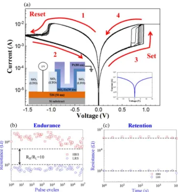
Fig. 1(a) shows bipolar resistance switching characteristics of the Pt/Zn : SiOx/TiN device for dc voltage sweep operations. The current–voltage (I–V ) properties of the sputtered SiO2
layer cannot exhibit the RRAM properties due to its superior insulating properties shown in the lower right inset in Fig. 1(a). The voltage sweep bias was applied on the TiN electrode with the grounded Pt electrode shown in the lower left inset in Fig. 1(a). In particular, the device can exhibit resistive switching behavior without forming process, which is different to most of RRAM devices. In the initial state, the resistance state of
400 IEEE ELECTRON DEVICE LETTERS, VOL. 34, NO. 3, MARCH 2013
Fig. 1. (a) Bipolar resistance switching current–voltage (I–V ) curves of the Pt/Zn : SiOx/TiN device with compliance current of 10 mA. The bottom left
inset shows the schematic diagram measured with grounded Pt electrode. The bottom right inset shows the I–V curve of the Pt/SiO2/TiN device.
(b) Endurance and (c) retention properties of Pt/Zn : SiOx/TiN memory
device. Read voltage was 0.1 V.
the Zn : SiOxdevice was at low-resistance state (LRS). As the voltage was swept from 0 to−1.6 V without current compli-ance, an abrupt decrease in current was observed, where the cell switches to high-resistance state (HRS) from LRS, called as “reset process.” In contrast, by sweeping the voltage from 0 to 1.3 V with a 10-mA current compliance, the resistance switched from HRS to LRS, called as “set process.” Moreover, the programming current of the device can be complied by integrating a selecting transistor.
To further investigate the reliability properties of the NVM device, endurance and retention tests were evaluated in Fig. 1(b) and (c), respectively. For endurance tests, the HRS was switched to the LRS by applying a set voltage of 1.5 V for 10 ns, while the LRS was reset to the HRS by applying a reset voltage of−2 V for 15 ns. This resistive switching speed is competing with the operation speed of static random access memory. Both HRS and LRS resistance values were extracted at 0.1 V. The resistance ratio between the HRS and the LRS was about ten times and can be maintained during the 107cycling bias pulse operations. The retention performance of the memory device was evaluated at 85◦C by measuring the resistance values of the LRS and HRS at 0.1 V with an interval. The resistance values of LRS and HRS remain almost constant even after 104s. This implicates that the resistance state did not vary easily due to oxygen diffusion under retention test.
The HRS and the LRS of I–V curves were analyzed for the current conduction mechanisms to further discuss the resistance switching mechanisms in the Zn : SiOxthin film (Fig. 2). The blue-square symbol in the I–V curve reveals that the current conduction in the HRS was dominated by the Poole–Frenkel conduction mechanism, followed by Ohm’s law with the square
Fig. 2. I–V curve fitting of Pt/Zn : SiOx/TiN memory device with various
carrier transport mechanisms in different bias regions and resistance states.
Fig. 3. FTIR spectra of Zn : SiOx film measured in middle infrared region.
The XPS spectra of Zn 2P3/2, Si 2P3/2, and O 1s core levels in Zn : SiOxfilm
are shown in the insets.
root of the applied voltage at high fields (the lower right inset in Fig. 2). The ohmic conduction occurred at the green-triangle-marked region in the HRS due to intrinsic carrier in the silicon oxide (the lower left inset in Fig. 2). Moreover, the current conduction in the LRS complied with the ohmic conduction mechanism.
To analyze the influence of Zn doping on resistance switch-ing characteristics in silicon oxide thin films, Fourier transform infrared spectroscopy (FTIR) was used to investigate the chem-ical bonding of the Zn : SiOxfilm in this study. Fig. 3 shows that the Si–O–Zn stretch bonding was found in the Zn : SiOxfilm at 1132 cm−1. In addition, the antisymmetric stretch mode and the symmetric stretch mode of Si–O–Si bonds were discovered at 1042 and 796 cm−1, respectively. According to these absorption peaks expressed in FTIR spectrums, we can confirm that the Zn element was bonded with the oxygen element in the silicon ox-ide film. To analyze the chemical composition of the Zn : SiOx film in this study, X-ray photoelectron spectroscopy (XPS) of Zn 2P3/2, Si 2P3/2, and O 1s peaks was performed, and the
XPS spectra are shown in the insets in Fig. 3. The mole frac-tion of Zn:Si:O in the Zn : SiOx film was 4.9%:24.9%:70.2% calculated from the peak areas of Zn, Si, and O XPS spectra. In addition, compared with the areas of deconvolution peaks of Zn 2P3/2 core levels, we found that the mole fraction of
CHANG et al.: CHARACTERISTICS AND MECHANISMS OF SILICON-OXIDE-BASED RRAM 401
Fig. 4. Schematic diagram of reaction model in Zn : SiOxfilm during resistive
switching operation of the device.
ZnO:Zn was 45.1%:54.9% in the Zn : SiOx film. The results of FTIR and XPS analyses demonstrated that the zinc metal is contained in the Zn : SiOxfilm and the Si–O–Zn stretch bonding is formed on the boundary of zinc metal and silicon oxide.
Based on the electrical and material analyses, we propose a reaction model to explain the resistive switching behavior of Zn-doped silicon-oxide-based RRAM in Fig. 4. As the sample was fabricated to the Pt/Zn : SiOx/TiN device, the zinc element was wrapped by silicon oxide, leading to the zinc conductive filament connecting with the two electrodes. Therefore, the electrical current is dominated by ohmic conduction in LRS of the device. Then, the conductive current causes the negative oxygen ion surrounding the conductive filament close to the Pt electrode to drift to the TiN electrode, oxidizing the zinc element to zinc oxide (ZnO). Hence, the electrical current will be obstructed by the ZnO region shown in Fig. 4, which will make the electrical current transfer to HRS in the RRAM device. In virtue of the boundary of ZnO and silicon oxide existing strained bonds, the conduction mechanism in HRS of the device complied with the Poole–Frenkel conduction [15].
IV. CONCLUSION
In conclusion, the reproducible forming-free bipolar resis-tance switching characteristics have been achieved by doping Zn metal into silicon oxide film using cosputtering technique at room temperature. According to electrical and material anal-yses, the current transport mechanism of LRS in Zn : SiOx RRAM was governed by ohmic conduction due to the con-ductive filament. Additionally, the current transport mechanism of HRS in Zn : SiOx RRAM was governed by Poole–Frenkel conduction, which was attributed to the strained bonds at the boundary of ZnO and silicon oxide nearby the TiN electrode. Based on the reliability evaluation, the Zn : SiOxRRAM satis-fied the demand of modern NVMs.
ACKNOWLEDGMENT
This work was performed at the National Science Coun-cil Core FaCoun-cilities Laboratory for Science and Nano-Technology in the Kaohsiung–Pingtung area.
REFERENCES
[1] T. C. Chang, F. Y. Jian, S. C. Chen, and Y. T. Tsai, “Developments in nanocrystal memory,” Mater. Today, vol. 14, no. 12, pp. 608–615, Dec. 2011.
[2] F. M. Yang, T. C. Chang, P. T. Liu, P. H. Yeh, Y. C. Yu, J. Y. Lin, S. M. Sze, and J. C. Lou, “Memory characteristics of Co nanocrystal memory device with HfO2as blocking oxide,” Appl. Phys. Lett., vol. 90,
no. 13, pp. 132102-1–132102-3, Mar. 2007.
[3] J. Liu, Q. Wang, S. B. Long, M. H. Zhang, and M. Liu, “Metal/Al2O3/
ZrO2/SiO2/Si (MAZOS) structure for high-performance non-volatile
memory application,” Semicond. Sci. Technol., vol. 25, no. 5, p. 055013, May 2010.
[4] F. M. Yang, T. C. Chang, P. T. Liu, U. S. Chen, P. H. Yeh, Y. C. Yu, J. Y. Lin, S. M. Sze, and J. C. Lou, “Nickel nanocrystals with HfO2
blocking oxide for nonvolatile memory application,” Appl. Phys. Lett., vol. 90, no. 22, pp. 222104-1–222104-3, May 2007.
[5] K. C. Chang, T. M. Tsai, T. C. Chang, Y. E. Syu, S. L. Chuang, C. H. Li, D. S. Gan, and S. M. Sze, “The effect of silicon oxide based RRAM with tin doping,” Electrochem. Solid-State Lett., vol. 15, no. 3, pp. H65–H68, Dec. 2011.
[6] Y. E. Syu, T. C. Chang, T. M. Tsai, Y. C. Hung, K. C. Chang, M. J. Tsai, M. J. Kao, and S. M. Sze, “Redox reaction switching mechanism in RRAM device with Pt/CoSiOX/TiN structure,” IEEE Electron Device
Lett., vol. 32, no. 4, pp. 545–547, Apr. 2011.
[7] K. C. Chang, T. M. Tsai, T. C. Chang, Y. E. Syu, C. C. Wang, S. L. Chuang, C. H. Li, D. S. Gan, and S. M. Sze, “Reducing operation current of Ni-doped silicon oxide resistance random access memory by supercritical CO2 fluid treatment,” Appl. Phys. Lett., vol. 99, no. 26,
pp. 263501-1–263501-4, Dec. 2011.
[8] Q. Liu, C. M. Dou, Y. Wang, S. B. Long, W. Wang, M. Liu, M. H. Zhang, and J. N. Chen, “Formation of multiple conductive fila-ments in the Cu/ZrO2: Cu/Pt device,” Appl. Phys. Lett., vol. 95, no. 2,
pp. 023501-1–023501-3, Jul. 2009.
[9] S. Zhang, S. B. Long, W. H. Guan, Q. Liu, Q. Wang, and M. Liu, “Resis-tive switching characteristics of MnOx-based ReRAM,” J. Phys. D, Appl.
Phys., vol. 42, no. 5, p. 055112, Mar. 2009.
[10] Y. Wang, Q. Liu, S. B. Long, W. Wang, Q. Wang, M. H. Zhang, S. Zhang, Y. T. Li, Q. Y. Zuo, J. H. Yang, and M. Liu, “Investigation of resistive switching in Cu-doped HfO2thin film for multilevel non-volatile memory
applications,” Nanotechnology, vol. 21, no. 4, p. 045202, Jan. 2010. [11] R. Huang, L. J. Zhang, D. J. Gao, Y. Pan, S. Q. Qin, P. R. Tang, Y. M. Cai,
and Y. Y. Wang, “Resistive switching of silicon-rich-oxide featuring high compatibility with CMOS technology for 3D stackable and embedded applications,” Appl. Phys. A, vol. 102, no. 4, pp. 927–931, Apr. 2011. [12] C. Y. Liu and P. W. Sung, “Different resistive switching characteristics of
a Cu/SiO2/Pt structure,” Jpn. J. Appl. Phys. 1, Regul. Rap. Short Notes,
vol. 50, no. 9, pp. 091101-1–091101-4, Sep. 2011.
[13] K. C. Chang, T. M. Tsai, T. C. Chang, Y. E. Syu, H. C. Hung, Y. C. Hung, T. F. Young, D. S. Gan, and N. J. Ho, “Low-temperature synthesis of ZnO nanotubes by supercritical CO2fluid treatment,” Electrochem. Solid-State
Lett., vol. 14, no. 9, pp. K47–K50, June 2011.
[14] T. C. Chen, T. C. Chang, C. T. Tsai, T. Y. Hsieh, S. C. Chen, C. S. Lin, M. C. Hung, C. H. Tu, J. J. Chang, and P. L. Chen, “Behaviors of InGaZnO thin film transistor under illuminated positive gate-bias stress,” Appl.
Phys. Lett., vol. 97, no. 11, pp. 112104-1–112104-3, Sep. 2010.
[15] S. Habermehl and C. Carmignani, “Correlation of charge transport to local atomic strain in Si-rich silicon nitride thin films,” Appl. Phys. Lett., vol. 80, no. 2, pp. 261–263, Jan. 2002.