2043
DC-RF
Performance
Improvement
for
Strained
0.13
gm MOSFETs
mounted
on a
Flexible Plastic Substrate
H. L.
Kaol,
Albert
Chin',
C. C.
Liao',
Y. Y.
Tseng',
S. P.
McAlister2 and
C. C.
Chi3
'Nano
Science Tech.
Center, Dept. of Electronics Eng., Nat'l
Chiao-Tung Univ.,
Univ.
System of
Taiwan,
Hsinchu,
Taiwan,
ROC
C2
National
Research Council of
Canada, Ottawa,
Canada
3Dept.
of
Physics, National
Tsing
Hua
Univ.,
Hsinchu, Taiwan,
ROC
Abstract - Byapplying 0.7% tensile strain to the flexible die
of a 0.13gmthin-body (40gm)Si MOSFET mounted on plastic,
both the DC and RF performance have been improved. The currentIdsatwas 14.3% higher, andfTincreased from 103 to 118 GHz with NFmi, decreasing from 0.89 to 0.75 dB at 10 GHz. These improvements are comparable with those forSiN-capped
90 nm strained-Si nMOS and consistent with device simulations. The approach has theadvantages of better RFpassivedevices on theinsulating plasticsubstrate and low cost.
Index Terms -RFNoise,associatedgain, MOSFET, plastic.
I.INTRODUCTION
The major technologychallenges for SiRFICscompared
with theirIll-V counterpartsarethe lowerperformance of the
activeRFtransistors [1]-[8], andlarge loss and noise from the
passive devices [9]-[13]. One method to overcome the large
RF loss from the passive devices is to integrate RF ICs on
insulating plastic. This provides lowerRF loss than thepoorly
isolating VLSI-standard Si substrates, andat alower cost
[1]-[3]. Thin-body Si ICs on plastic can be used for Flexible
Electronics, RF ID, wireless Displays and System-on-Plastic
[2]-[3], [14], since no practical flexible polymer or organic
transistors have been demonstrated for the RF regime.
Additionally, the RF performance of0.18 tm thin-body (30
gim)
Si MOSFETs can be improved by applying mechanicalstrain, whichnarrowsthe performance gapbetween them and
Ill-V transistors [2]-[3]. Here we report the DC to RF
performance of0.13 gm thin-body (40
gim)
Si MOSFETs onplastic, aiming to improve the RF performance. Using a
microstrip line layout, to shield the RF noise from the low
resistivity Si substrate [2]-[4], good performance, in terms of
the minimum noise figure (NFmin), associatedgainand cut-off
frequency
(fT)
was measured for the 0.13 gm MOSFETsmounted on plastic. The data were close to those for control
0.13 gm devices, indicating littleprocess-related degradation.
The DC-RF performances were enhanced by applying
0.70O
tensile strain. Theimprovement of the saturation drain current
(Id,sat)
in the mechanically-strained 0.13 tm device (14.3%)was higher than that for SiN-capped, 90nmnode, strained-Si
nMOS (1II%) [15], and hada lowNFmini(0.75 dB at 10GHz)
due to the microstrip line layout [4]. The improved DC-RF
performance was confirmed by T-Supreme and Medici
simulations (TMA). The improvements arise from the thin
body thickness(tb) and high flexibility, since the surface strain
increases with 1/tb2 [16]. The RF noise improvement fits an
analytical NFmin equation well [8], and it is duetothe increase
ing,, and theRFgain under strain.
II.EXPERIMENTAL PROCEDURE
Multiple-gate-finger (8, 16, and 32) 0.13 tm MOSFETs
[6]-[8] withanovelmicrostrip line layout [2]-[4]wereusedin
this study. The multiple-gate-finger structure was used to
reduce the gate-resistance-generated thermal noise and the
microstrip line layouts were designed using Metal-I as the
ground plane to reduce the RF noise from the lossy Si
substrate [3]. To achieve integration onto
plastic,
we firstthinned down the Si substrate from500 tm to40 tmby using
a Chemical Mechanical Polish (CMP) procedure. The thinned
die was then glued onto a 180 tm thick light-transparent
polyethyleneterephthalate (PET) plasticasshowninFig. l(a).
Theplastic had aresistivity of109 Q-cm. Figure l(b) shows
the40 tm Si substrate underalarge surface strain. Thus, it is
possibleto apply a large mechanical strain to the flexible Si
substrate devices onplastic andnotcrack the Si substrate. We
have calculated the surface strain by using ANSYS 8.0
simulation software and the device characteristics, under
various applied tensile strains, using TMA process-device
simulation software.
The device characteristics were measured using an
HP4 155C for DC,HP851OC networkanalyzer for S-parameter andATN-NP5Bfor noisemeasurements[6]-[8].
(a)
(b)
Fig. 1. (a)
Inage
ofa die withmultiple-gate-finger 0.13Rim
RF MOSFETsontransparentplastic (hand-held). (b)Inage
showingthe flexibility of the -40 rim-thick Si substrate (tb) under mechanical strain(which isproportionalto1/tb2).2044 III.RESULTS ANDDISCUSSION
A. DC-RFPerformanceonplastic.
Figure 2 shows a comparison of DC Id-Vg and Id-Vd
characteristics for the 16-gate-fingern-MOSFET on a
VLSI-standard substrate and on plastic with the 40 tm Si. The
measuredId-VgandId-Vdof the0.13 tm devices, before and
after thinning and mounting on plastic, is almost identical.
Thus there is little degradation resulting from the
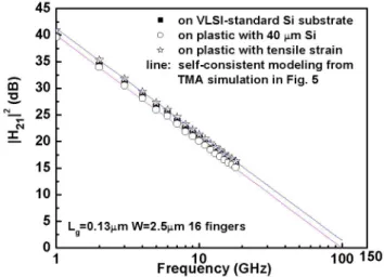
thinning-down process and mounting on plastic. Similarly, little
change appeared inthe measured
JH21
2 RF gain for the 0.13tmMOSFETs, before and afterthinning down and mounting,
as depicted inFig. 3. These results representan improvement
over the previous ICP etching and thinning process [2]-[3]
since theCMPtechnique avoids plasmadamage. Good device
performance is indicatedbyafTof 103 GHz for the 0.13 tm
RFMOSFETs. l o-,E 10-3 E __p 10-5 10-7 10-9L 0. Lg=0.13grmW=2.5gtm16fingers measure@Vd=0.1V. * on VLSI-standard Si substrate * on plastic with 40gtmSi * onplasticwith tensile strain line: simulationby TMA
0.2 0.4 0.6 0.8 1.0 1.2 Vg M (a) JoI. - -- . - --.-30 25 < 2o a/^
~~~~~~~~~~~~~~~~~~~~~g_
5 0 0.0 0.2 0.4 0.6 0.8 1.0 1.2 Vd (V) (b)Fig. 2. (a) Measured and simulated IdJVgcharacteristics and(b)Id-Vd
for t6-gate-finger 0.13 Rim RF MOSFETs on a VLSI-standard
substrate andonplasticwith 40Rim Si, withorwithout tensile strain.
The solid lines arethe TMA-simulated data for aVLSI-standard Si
substrate andonplasticunder 0.7%tensile strain.
m ~0 I 4l 40 35 30 25 20 15 101 5 n v1
Frequency (GHz)
~~10 100 150Fig. 3. Measured and simulated
JH2112
as afunction offrequency for 16-gate-finger0.13 Rim RFMOSFETs on aVLSI-standard substrate andonplastic with40 Rim Si withorwithout tensile strain. The line is the modeled data.B. DC characteristics enhancementbystrain.
Byexploiting the flexibility of the thin substrate,wehave
applied a tensile stress to the MOSFETs die on plastic. The
10 large surface strain(g
3aF/btb2E)
[15]results from the applied uEz force (F) associated with the bending distance (a) and widthE (b). Figure 4 shows the thin Si substrate under an applied
longitudinal tensile strain, as calculated using ANSYS 8.0
5 simulation software. Thebending distance was0.17 cm when
using 0.8 GPa stress on 40 tm thick Si substrate. This
condition gives a tensile strain of 0.700 (= 0.8GPa/115GPa),
assuming that the Young's Modulus of Si is 115GPa.
n
AN
DEC 1 2005 a =0.17cm Stress=0.8GPa BendingdistanceFig. 4. The mechanical stress calculated by using ANSYS 8.0
simulation software.
Under the same conditions, the experimental data of the
effect of strain on the DC characteristics are also shown in
Figs. 2(a) and 2(b). Afterapplying a -0.700 tensile strain, the
thin-Si body MOSFETs on plastic showed a 0.045V lower
thresholdvoltage(Vth)anda 14.3%higher
Id,sat.
NOA SO OION 51TEP=l SUE -1 TI!E=1l 'UZ (AVr,) pksT =o DM=.01277 5M:c =.A0177s * onVLSI-standard Sisubstrate o onplastic with 40gmSi * onplastic with tensile strain line: self-consistent modelingfrom
TMAsimulation in Fig. 5
-Lg=0.13gmW=2.5gm16fingers
L=0.13gmW=2.5gm 16tingers
* onVLSI-standard Si substrate o on plasticwith 40gmSi
* on plasticwith tensile strain -line: simulation byTMA
u "". V __ _ I*v. 4. 0 V =1.3Vgs
2045 To understand the improvements, we have used TMA process-device simulation software to simulate the effect of
strain on the 0.13 tm MOSFETs. The simulated stress
distribution is shown in Fig. 5. A good match between the
measured and simulated Id-Vg and Id-Vd results were first
achieved for the unstrained case to show the accuracy of the
TMA simulation and theyareincluded inFigs. l(a) and l(b),
respectively. Then effect of strain on 0.13 tm transistors
themselveswas simulated. Figure6 summarizes the measured
and simulated
Id,sat
improvement as a function of strain. Thestrain lowers
Vlh
(=OMS-QOX
COX+20F+Qdp1
Co,)
because itreduces the energy band-gap (EG) and thus
OF
and Qdpl. Asignificant Id,sat improvement (14.3%) was seen compared
withSiN-capped90nmstrained-SinMOS,where the increase
was 11% [15]. The effect arises from the 1/tb2 dependence of
the strain forthin-body Si. This shows that both the lowerRF
loss for the passive devices and a higher transistor drive
current can be obtained simultaneously using the mechanical
strain made possible by using highly-insulating plastic
substrates.
C. EnhancementoftheRFcharacteristics bystrain.
Fig. 3 includes the dependence of the RF current gain
JH2112
withfrequency,
for a 16-gate-finger 0.13 gm device with tensile strain, was.JH21
2 follows the typical -20dB/decade slope with increasing frequency. After applying a
0.700 tensile strain to the 40 tm thinned-body Si of the
0.13gm RF MOSFETs,fT increased from 103 GHz to 118
GHz. These improvements were consistent with the
simulations, whichareincludedinFig. 3.
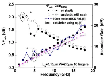
We also investigated how strain affects the RF noise.
Figure 7 shows NFmin and the associated gain of the 0.13tm
transistors under tensile strain.Forthe unstrainedcase, agood
NFmin of 0.89 dB and associated gain of14.2 dB at 10 GHz
wasobserved. Under theapplied 0.70o tensile strain, betterRF
characteristics were achieved, such as alower 0.75 dB NFmin
and a higher 15.3 dB associated gain at 10 GHz. This is
related to the larger gmn, smaller Vth and higher
Idcsat
arisingfrom the strain, as shown in Fig. 2. The lower NFmin arises
because [2]-[3]:
NFmin_ 1+2y(1 +gmRgly)5ffT
(1)
and that the strain improved the fT. The close agreement
between the measured and simulatedNFmin alsoappearsinFig.
7. The detailed device parameters weused aresummarizedin
Table I. The improved NFmin and associated gain values are
comparable with those for 90nmnode SiN-capped strained-Si
nMOS [5], and also depicted in Fig. 7. The large DC-RF
improvements with tensile strain arethe main advantages of
thin-Si-body flexible electronics on plastic, in addition to the
improvedRFpassive deviceperformance[1]-[3].
=-D KIC I;a JU
2.0k
Fig. 5. TMA device simulation ofa40 tm Si-body 0.13 tm
RFMOSFETsunderapplied mechanical strain.
0.0 0.2 0.4 0.6 Strain(%)0.8 1.0 1.2 n in m E-z 1.51- 1.01- 0.51-0.34 n n 0 0.32 5 10 15 20 Frequency (GHz) m 20 -._ co ._v 10 o en en n
Fig. 7. Measured and modeled NFmin and associated gain of 16-gate-finger 0.13 Rim RF MOSFETs on plastic and 40 Rim Si, with or
without tensile strain. Theline is the TMA-modeled data and derived
from theNFmin equation.
ni2n
Fig. 6. Simulated (shown red) and measured (shown black)
Id,at
and V/hversusstrain. The strain increasesId,sat
but decreasesV/h.28 26 E -P24 22 Nlmin uainASSO , * * onplastic .QOXl n o on plastic, with strain
,. -A-90nm mode nMOS Ref.[5]
line: simulationusing eq. (1)
A-o. 0.13mW25m1 igr g F9 ._. 0 A ~ ~~ _ . IJ Lg=0.13itmW=2.5,tm 16fingersVthextracted | Vd=O.lV&ld=¶l
oSQlid:Measured Open:TMASimulated
A
'd~measuredd,sat~~~~ ~Vg=1.3V,V=13
A- .- .. --t . -.1
U_ _
2046
TableI. Inportantdevice parameters of body-thinned 16-gate-finger 0.13 Rtm RF MOFSETs,before and after strain.
before strain after strain
fT(GHz)
103 118y 1.0 1.0
gm
(S)
0.025 0.032Rg
(Q)
9.6 9.6IV.CONCLUSIONS
We have successfully demonstrated high DC and RF performance for 0.13 tm RF MOSFETs on 40 tm Si
substrates mounted on a flexible plastic base. These devices
showed excellent DC and RF performance after applying tensile strain to the thinned-down substrate. The high performance RF transistors are suitable for low-noise
ultra-wide band(UWB) (3.1-10.6 GHz) applications. ACKNOWLEDGEMENT
The authors at Taiwan would like to thank the Chip Implemental Center (CIC) and G. W. Huang's group at
National Nano-Device Lab. for their help and the RF
measurements.
REFERENCES
[1] R.Dekker, K. Dessein, J.-H. Fock, A. Gakis, C. Jonville, 0.M.
Kuijken, T. M. Michielsen, P. Mijlemans, H. Pohlmann, W. Schnitt, C. E. Timmering, and A. M. H. Tombeur, "Substrate transfer: enabling technology for RF applications," Int. Electron Devices Meeting (IEDM) Tech. Dig., pp. 371-374,
Dec. 2003.
[2] H. L.Kao, A. Chin, C. C. Huang, B. F. Hung, K. C. Chiang, Z. M. Lai, S. P. McAlister and C. C. Chi, "Low Noise and High GainRF MOSFETs onPlastic Substrates," IEEEMTT-SInt.
MicrowaveSymp. Dig.,pp.295-298, June 2005.
[3] H. L.Kao, A. Chin, B. F. Hung, J. M. Lai, C. F. Lee, M.-F. Li, G. S. Samudra, C. Zhu, Z. L. Xia and J. F. Kang, "Strain-Induced Very Low Noise RF MOSFETs on Flexible Plastic
Substrate," Symp. on VLSITech.,pp. 160-161, June 2005.
[4] H. L.Kao, A. Chin, J. M. Lai, C. F. Lee, K. C. Chiang and S. P. McAlister, "Modeling RF MOSFETs After Electrical Stress Using Low-Noise Microstrip Line Layout," RF IC Symp. Dig.,
pp.157-160, June 2005.
[5] K. Kuhn, R. Basco, D. Becher, M. Hattendorf, P. Packan, I.
Post, P. Vandervoom andI.Young, "A comparison of
state-of-the art NMOS and SiGe HBT devices for analog/mixed-signal/RF circuit applications," in Symp. On VLSI Tech., pp. 224-225, 2004.
[6] C. H. Huang, K. T. Chan, C. Y. Chen,A. Chin, G. W. Huang, C. Tseng, V. Liang, J. K. Chen, and S. C. Chien, "The
minimum noise figure and mechanism as scaling RF MOSFETs from 0.18 to 0.13 Rim technology nodes,"in IEEE RFICSymp.,pp. 373-376, 2003.
[7] M.C. King, M. T.Yang,C. W. Kuo, Y. Chang, andA. Chin,
"RFnoisescaling trend of MOSFETs from 0.5Rimto 0.13 Rim technology nodes," IEEEMTT-S Int. Microwave Symp. Dig., pp.6-11,2004.
[8] M.C.King,Z. M. Lai, C. H. Huang, C. F. Lee, M. W. Ma, C. M. Huang, Y. Chang andA. Chin, "Modeling finger number dependence on RF noise to 10 GHz in 0.13 Rtm node MOSFETs with 80nm gatelength," IEEE RFIC Symp. Dig., pp. 171-174, 2004.
[9] D. S. Yu, K. T. Chan, A. Chin, S. P.McAlister, C.Zhu,M. F.
Li, and Dim-Lee Kwong, "Narrow-band band-pass filters on
silicon substrates at 30 GHz," IEEE MIT-S Int. Microwave
Symp.Dig., pp. 1467-1470,June2004.
[10] A. Chin, K. T. Chan, H. C. Huang, C. Chen, V. Liang, J. K.
Chen, S. C. Chien, S. W. Sun, D. S. Duh, W. J. Lin, C. Zhu,
M.-F. Li, S. P. McAlister and D. L. Kwong, "RF passive devicesonSi with excellentperformance closetoideal devices
designed by electro-magnetic simulation,"in IEDMTech. Dig,
2003,pp.375-378.
[11] K. T. Chan,A. Chin,Y. B. Chen,Y.-D.Lin,D. T. S.Duh, and
W. J. Lin, "Integratedantennas onSi, proton-implanted Si and Si-on-Quartz,"in IEDMTech. Dig,2001,pp.903-906.
[12] K. T. Chan,A. Chin, C. M.Kwei, D. T. Shien, andW. J. Lin
"Transmission line noise from standard and proton-implanted Si,"IEEEMTT-S Int. MicrowaveSymp. Dig., vol. 2,pp.
763-766,June2001.
[13] Y. H. Wu,A.Chin,K. H.Shih, C. C. Wu, S. C.Pai, C. C.Chi, and C. P. Liao, "RF loss and cross talk on extremely high resistivity (IOK-IMQ-cm) Si fabricated by ion implantation,"
IEEEMTT-S Int. MicrowaveSymp. Dig., vol. 1, pp.221-224,
June2000.
[14] T. Takayama, Y. Ohno, Y. Goto, A. Machida, M. Fujita, J.
Maruyama,K.Kato, J.Koyama,andS. Yamazaki,"ACPU on a plastic film substrate," Symp. on VLSI Tech., pp. 230-231,
June2004.
[15] T. Ghani,M.Armstron,C.Auth,M.Bost,P.Charvat,G.Glass,
T.Hoffmann,K.Johnson,C. Kenyon, J.Klaus,B.Mclntyre,K.
Mistry,A.Murthy,J. Sandford,M.Silberstein,S. Sivakumar,P.
Smith, K. Zawadzki, S. Thompson, and M. Bohr, "A 90nm high volume manufacturing logic technology featuring novel
45nm gate length strained silicon CMOS transistors," Int.
Electron Devices Meeting (IEDM) Tech. Dig., pp.
11.6.1-11.6.3,Dec.2003.
[16] W. Zhao, J. He, R. E. Belford, L.-E. Wernersson, and A.
Seabaugh, "Partially depleted SOI MOSFETs under uniaxial tensilestrain,"IEEETrans.Electron Devices, vol. 54,pp.