Deep level transient spectroscopy characterization of InAs self-assembled quantum
dots
V. V. Ilchenko, S. D. Lin, C. P. Lee, and O. V. Tretyak
Citation: Journal of Applied Physics 89, 1172 (2001); doi: 10.1063/1.1336519 View online: http://dx.doi.org/10.1063/1.1336519
View Table of Contents: http://scitation.aip.org/content/aip/journal/jap/89/2?ver=pdfcov
Published by the AIP Publishing
Articles you may be interested in
Deep levels in GaAs(001)/InAs/InGaAs/GaAs self-assembled quantum dot structures and their effect on quantum dot devices
J. Appl. Phys. 107, 073111 (2010); 10.1063/1.3359704
Combined optical and electrical studies of the effects of annealing on the intrinsic states and deep levels in a self-assembled InAs quantum-dot structure
J. Appl. Phys. 100, 043703 (2006); 10.1063/1.2234817
Conduction band offset in InAs/GaAs self-organized quantum dots measured by deep level transient spectroscopy
Appl. Phys. Lett. 76, 2571 (2000); 10.1063/1.126411
Tuning the energy levels of self-assembled InAs quantum dots by rapid thermal annealing
Appl. Phys. Lett. 76, 691 (2000); 10.1063/1.125863
Near-field magneto-optical spectroscopy of single self-assembled InAs quantum dots
Appl. Phys. Lett. 73, 517 (1998); 10.1063/1.121919
[This article is copyrighted as indicated in the article. Reuse of AIP content is subject to the terms at: http://scitation.aip.org/termsconditions. Downloaded to ] IP: 140.113.38.11 On: Thu, 01 May 2014 07:19:52
Deep level transient spectroscopy characterization of InAs self-assembled
quantum dots
V. V. Ilchenko, S. D. Lin, and C. P. Leea)
Department of Electronics Engineering, National Chiao Tung University, 1001 Ta Hsueh Road, Hsinchu, Taiwan, Rebpublic of China
O. V. Tretyak
Faculty of Radiophysics of Kiev Taras Shevchenko University, 64 Vladimirskaya Street, Kiev, Ukraine
共Received 3 July 2000; accepted for publication 3 November 2000兲
Deep level transient spectroscopy 共DLTS兲 was used to obtain the energy level and the capture characteristics of InAs self-assembled quantum dots embedded in GaAs. A specially designed structure was used for the DLTS measurement for enhanced resolution. This structure allows us to detect capacitance relaxation signal from a single layer of quantum dots and to separate this signal from those of the DX centers inside the structure. The DLTS spectra with different filling pulses and different rate windows provide clear information on the energy level and the capture characteristics of the quantum dots. © 2001 American Institute of Physics. 关DOI: 10.1063/1.1336519兴
I. INTRODUCTION
Considerable interest has recently been focused on char-acterization of self-organized quantum dots共QD兲.1–8In order to develop a new generation of devices such as QD lasers, optical memory elements, and resonant-tunneling devices based on quantum dots, it is very important to have a com-plete understanding of the physical properties of the QDs. To obtain information about energy levels of quantum dots, op-tical methods such as photoluminescence共PL兲4–6are usually used. Recently, deep level transient spectroscopy 共DLTS兲 has also been used.1–3,9,10In principal the DLTS method has some advantages over conventional optical methods. The transient capacitance techniques are able not only to detect levels of quantum dots, but also unambiguously to determine their capture parameters. However, investigation of a single layer of QDs in ordinary Schottky-diode structures by means of DLTS has been difficult because of small or not clear relaxation signals. The DLTS spectras on QDs reported in the literature usually dealt with multiple layers of QDs.2 In this article we describe a structure, which contains a GaAs–Al0.35Ga0.65As heterojunction, for the DLTS investi-gation of a single layer of QDs. It enables us to obtain very clear and unambiguous DLTS signals of the QDs. Because of the presence of the second potential barrier, which is pro-vided by the GaAs/Al0.35Ga0.65As heterojunction not far from the QDs, the structure allows us to easily change the extent of filling of the QDs and to obtain the signals.
II. EXPERIMENT DATA AND DISCUSSION OF RESULTS
A. Samples and method of study
The samples used for this study were grown by molecu-lar beam epitaxy using a Varian GEN II system. The struc-ture consisted of, starting from the共100兲 n⫹-GaAs substrate, a Si-doped n⫹-GaAs buffer layer, an n⫹-Al0.35Ga0.65As
layer (2⫻1018 cm⫺3, 300 nm兲, an n⫹-Al0.35Ga0.65As layer
(1⫻1017 cm⫺3, 150 nm兲, a 10 nm n-type graded
AlxGa1⫺xAs layer, an n-GaAs space layer (3.5⫻1015cm⫺3, 30 nm兲, an undoped InAs quantum dot layer 共2.6 ML兲, and an n-GaAs layer (n⫽3.5⫻1015 cm⫺3, 270 nm兲. The struc-ture and the band diagram are schematically shown in Fig. 1. The growth rate of InAs quantum dots was about 0.1 ML/s and the growth temperature was 520 °C. To improve the uni-formity of the dot size, we interrupted the In flux for 6 s for every 0.2 ML. After the layers were grown, Ti/Au Schottky diodes with a size of 1.44⫻10⫺3cm2were formed for DLTS measurement by standard lithographic technique. The back ohmic contact was formed by alloying In to the n⫹-GaAs substrate. The quantum dot formation was confirmed by the atomic force microscope 共AFM兲 image 共see Fig. 2兲, which was taken after the dots were grown.
The additional GaAs/Al0.35Ga0.65As heterobarrier under-neath the QDs of this specially designed structure has two purposes: 共1兲 to create conditions under which all QD states can be completely filled at zero or small negative offset volt-ages, and共2兲 to provide a more desirable voltage distribution near the quantum dot layer to facilitate the filling and escap-ing processes for electrons in the quantum dots durescap-ing DLTS measurement.
The DLTS measurement was carried out using a MI-401 Megabytec DLTS spectrometer. Low temperature 共at 20 K兲 photoluminescence共PL兲 spectra were measured using argon laser for excitation. InGaAs detector and a Si-PMT were used for light detection.
B. Result and discussion
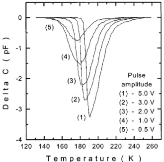
All the DLTS measurements were performed by direct determination of the electron emission rate as a function of temperature from 80 to 472 K in a wide range of time win-dow from 10⫺6 to 10⫺1s under dark condition. Before each scan, the sample was cooled down under zero bias and the measurements were made during the warm up cycle. Figure 3 shows the measured DLTS spectra with different filling
a兲Electronic mail: [email protected]
JOURNAL OF APPLIED PHYSICS VOLUME 89, NUMBER 2 15 JANUARY 2001
1172
0021-8979/2001/89(2)/1172/3/$18.00 © 2001 American Institute of Physics
[This article is copyrighted as indicated in the article. Reuse of AIP content is subject to the terms at: http://scitation.aip.org/termsconditions. Downloaded to ] IP: 140.113.38.11 On: Thu, 01 May 2014 07:19:52
pulses. The rate window was 3.4⫻10⫺4 s and the offset voltage was ⫺5.5 V. To vary the average occupation of the dots, the amplitude and the duration of the filling pulses were varied. DLTS signals关curves 共1–3兲 in Fig. 3兴 from the quan-tum dots were clearly observed when the positive filling pulses were more than 3 V with different duration of filling pulses. In cases when the filling pulses were smaller and long, wider and more symmetric DLTS signals共curves 4 and 5兲 were obtained. These signals were observed in all samples with and without QDs and they had distinctly different physical characteristics. We suppose these signals are attrib-uted to the well-known DX centers in the Al0.35Ga0.65As layer.11,12To separate parentage of different peaks we have also prepared a similar structure but without quantum dots. In this case, all the quantum dot peaks completely disap-peared. Only the DLTS signal from those related to DX cen-ters remained. Besides, the signal from these cencen-ters could be completely switched off by means of short filling pulses with duration less than 5⫻10⫺5 s because of the relatively small capture cross section of such kinds of defects. Figure 3 also shows that the position of the QDs DLTS peak varies with the height of the filling pulses when they are below 5 V and remains about the same when the pulse height is above 5 V. This is due to the shift in the energy level caused by the electric field from the offset voltage and the filling pulses.
From activation plots of these dependencies we determine the emission energies共see Fig. 4兲. The saturation point cor-responds to the flat band condition and the measured activa-tion energy gives an energy difference between the quantized level in the dots and the GaAs band edge to be 0.4 eV. Because of the excellent resolution of the DLTS spectrum, we were able to measure the capture characteristics of the QDs. The electron capture cross section and the quantum dot concentration were then calculated using the ordinary proce-dure for DLTS analysis to be 1.07⫻10⫺12 and 1.0⫻1010 cm⫺2, respectively. It should be mentioned that the cross section about 10⫺12 cm2is much higher than those of com-monly observed defects, and it is a good indication of the existence of quantum dots.
FIG. 3. DLTS spectra taken at a constant offset voltage of⫺5.5 V and a rate window of 3.4⫻10⫺4s with different amplitudes of filling pulses.
FIG. 4. Activation plot for DLTS signal from QDs with the 3.0–5.0 V pulses, and from DX centers obtained with the 0.5 V amplitude of filling pulses.
FIG. 1. Band diagram of the structure for DLTS measurements at zero offset voltage and layer structure of the quantum dot sample.
FIG. 2. AFM image of InAs islands.
1173
J. Appl. Phys., Vol. 89, No. 2, 15 January 2001 Ilchenkoet al.
[This article is copyrighted as indicated in the article. Reuse of AIP content is subject to the terms at: http://scitation.aip.org/termsconditions. Downloaded to ] IP: 140.113.38.11 On: Thu, 01 May 2014 07:19:52
Figure 5 shows the dependence of the amplitude DLTS signal on the duration of the filling pulse. The measurement was taken at a constant offset voltage of⫺5.5 V and a rate window of 3.4⫻10⫺4 s. The amplitude of the filling pulses was 5.0 V. The capture time can be obtained by fitting this dependence with the following equation13
C共tp兲⫺C共tp⫽⬁兲⫽C0exp
冉
⫺tptc
冊
, 共1兲
where C(tp) is the relaxation signal measured with a pulse width of tp, C(tp⫽⬁) is the relaxation signal when the pulse width is infinitely long to saturate the DLTS signal. tc is the time of capture, which can be expressed as t
c ⫽(vn)⫺1, where is the capture cross section, v is the electron’s thermal velocity, and n is the free electron concen-tration. The inset of Fig. 5 shows the fitted result. We see that experimental data of short enough duration of pulses followed Eq. 共1兲 very well. Time of capture of 3⫻10⫺6 s was calculated on the basis of this result.
We have studied the QDs using an atomic force micro-scope for as-grown InAs islands共Fig. 2兲. The average lateral size of the these islands is around 200 Å, and height of the islands is around 30 Å. Average concentration is about 1.25⫻1010cm2. These numbers agree with the concentration determined by DLTS.
The samples were characterized by photoluminescence. Figure 6 shows the 20 K PL spectra of the samples. The peak related to QDs ground state transition gives an energy of 1.08 eV. Combining the QD emission activation energy of 0.4 eV from DLTS with the energy of GaAs related emission 共1.52 eV兲 we can approximately estimate a very small band offset for holes.
III. CONCLUSIONS
In conclusion, we have used DLTS to characterize a single-layer of self-assembled InAs QDs. The excellent reso-lution of the DLTS signals was obtained by using a specially designed structure. The electron ground state energy of the quantum dots was unambiguously determined. The density of the QDs, the capture cross section and the capture time were also determined based on the DLTS results. The ob-tained results agree with those determined by other methods such as AFM and low temperature PL.
ACKNOWLEDGMENTS
This work was supported by the National Science Coun-cil under Contract No. NSC 89-2215-E-009-013 and the Lee-MTI Center of National Chiao Tung University.
1M. M. Sobolev, A. R. Kovsh, V. M. Ustinov, A. Yu. Egorov, A. E.
Zhukov, and Yu. G. Musikhin, Fiz. Tekh. Poluprovodn, 33, 184共1998兲
关Semiconductors 33, 157 共1999兲兴.
2H. L. Wang, D. Ning, H. J. Zhu, F. Chen, H. Wang, X. D. Wang, and S.
L. Feng, J. Cryst. Growth 208, 107共2000兲.
3S. Ghosh, B. Kochman, J. Singh, and P. Bhattacharya, Appl. Phys. Lett.
76, 2571共2000兲.
4
V. K. Kalevich, M. N. Tkachuk, P. Le Jeune, X. Marie, and T. Amand, Phys. Solid State 41, 789共1999兲.
5Y. Toda, S. Shinomori, K. Suzuki, and Y. Arakawa, Phys. Rev. B 58,
R10147共1998兲.
6
F. Y. Tsai and C. P. Lee, J. Appl. Phys. 84, 2624共1998兲.
7F. Chen, S. L. Feng, X. Z. Yang, Q. Zhao, Z. M. Wang, and L. S. Wen,
Phys. Low-Dimens. Semicond. Struct. 11Õ12, 179 共1997兲.
8P. N. Brunkov, A. A. Suvorova, N. A. Bert, A. R. Kovsh, A. E. Zhukov,
A. Yu. Egorov, V. M. Ustinov, A. F. Tsatsul’nikov, N. N. Ledentsov, P. S. Kop’ev, L. Eaves, and P. S. Main, Fiz. Tekh. Poluprovodn. 32, 1229
共1998兲 关Semiconductors 32, 1096 共1998兲兴.
9S. Anand, N. Carlsson, M.-E. Pistol, L. Samuelson, and W. Seifert, Appl.
Phys. Lett. 67, 3016共1995兲.
10
S. Anand, N. Carlsson, M.-E. Pistol, L. Samuelson, and W. Seifert, J. Appl. Phys. 84, 3747共1998兲.
11G. Grummt, R. Piekenhait, and L. Lehmann, Solid State Commun. 73, 257 共1990兲.
12P. M. Mooney, Semicond. Sci. Technol. 6, B1共1991兲. 13
J. A. Pals, Solid-State Electron. 17, 1139共1974兲.
FIG. 5. Dependence of the amplitude of DLTS signal on the duration of the filling pulses. The results of measurements were taken at a constant offset voltage of⫺5.5 V and amplitudes of filling pulses 5.0 V at different dura-tion of filling pulse.
FIG. 6. PL spectra of our sample.
1174 J. Appl. Phys., Vol. 89, No. 2, 15 January 2001 Ilchenkoet al.
[This article is copyrighted as indicated in the article. Reuse of AIP content is subject to the terms at: http://scitation.aip.org/termsconditions. Downloaded to ] IP: 140.113.38.11 On: Thu, 01 May 2014 07:19:52