國
立
交
通
大
學
電子工程學系 電子研究所
碩 士 論 文
考量可繞線度之晶片封裝共同設計下的界面凸塊規劃
Routability-Driven Bump Assignment
for Chip-Package Co-Design
研 究 生:陳孟伶
指導教授:陳宏明 博士
國
立
交
通
大
學
電子工程學系 電子研究所
碩 士 論 文
考量可繞線度之晶片封裝共同設計下的界面凸塊規劃
Routability-Driven Bump Assignment
for Chip-Package Co-Design
研 究 生:陳孟伶
指導教授:陳宏明 博士
考量可繞線度之晶片封裝共同設計下的界面凸塊規劃
Routability-Driven Bump Assignment
for Chip-Package Co-Design
研 究 生:陳孟伶 Student:Meng-Ling Chen
指導教授:陳宏明 博士 Advisor:Dr. Hung-Ming Chen
國 立 交 通 大 學
電子工程學系 電子研究所
碩 士 論 文
A Thesis
Submitted to Department of Electronics Engineering and Institute of Electronics
College of Electrical and Computer Engineering National Chiao Tung University
in partial Fulfillment of the Requirements for the Degree of
Master of Science in
Electronics Engineering
July 2013
Hsinchu, Taiwan, Republic of China
Acknowledgements
First, I would like to show my greatest appreciation to my advisor, Prof. Hung-Ming Chen, for the valuable guidance and advice. I have obtained a lot of abilities about research and technical writing from him. I also want to express my grati-tude to my intern supervisor in Global Unichip Corporation (GUC), Mr. Shi-Hao Chen, who had offered abundant help and support. This internship has given me the chance to gain knowledge about various industrial design tools. Without these knowledge and the assistance from GUC, this study would not have been successful. Besides, I want to thank all the members of the VLSI Design Automation Labora-tory, for their help and company for these years. Especially, I would like to express my special thanks to Tu-Hsung Tsai, Yi-En Chen, and Ching-Yu Chin, who con-tributed to this project. Finally, my thanks and appreciations also go to my families and friends for their understandings and supports on me in completing this project.
Meng-Ling Chen July, 2013
考
考
考量
量
量可
可
可繞
繞
繞線
線
線度
度之
度
之
之晶
晶
晶片
片
片封
封
封裝
裝
裝共
共同
共
同
同設
設
設計
計
計下
下
下的
的
的界
界
界面
面
面凸
凸
凸塊
塊
塊規
規
規劃
劃
劃
研究生:陳孟伶 指導教授:陳宏明 博士 國立交通大學電機學院電子工程研究所摘
摘
摘 要
要
要
在現今積體電路的晶片與封裝設計流程中,要同時在晶片、封裝、以及電路 板三個領域達到界面凸塊規劃與界面凸塊繞線的最佳化是一件非常困難的事情。 通常,整個設計流程需要大量的人力資源,除此之外,為了達到最佳化,工程師 必須反覆重新規劃界面凸塊與繞線,因而降低了產品獲利。基於上述原因,我們 針對晶片與封裝共同設計提出一個快速的啟發式演算法,以實現自動化界面凸塊 規劃的目標,而且,藉由此演算法所規劃的界面凸塊將能使晶片重分配層與封裝 繞線層具備很高的可繞線度(在我們的實際測試案件中達到了百分之百的可繞線 度)。實驗結果顯示,本論文中提出的演算法(由逃脫繞線演算法所啟發)可在很短 的時間內完成界面凸塊規劃、晶片重分配層繞線、以及封裝繞線;然而,傳統的 晶片與封裝共同設計流程卻要花費數個禮拜甚至好幾個月才能實現整個設計。 關鍵字:界面凸塊規劃、晶片與封裝共同設計、逃脫繞線、重分配層繞線、封 裝繞線、封裝布置規畫Routability-Driven Bump Assignment
for Chip-Package Co-Design
Student: Meng-Ling Chen Advisor: Dr. Hung-Ming Chen Graduate Institute of Electronics Engineering
College of Electrical and Computer Engineering National Chiao Tung University
ABSTRACT
In current chip and package designs, it is a bottleneck to simultaneously optimize both pin assignment and pin routing for different design domains (chip, package, and board). Usually, the whole process costs a huge manual effort and multiple iterations thus reducing profit margin. Therefore, we propose a fast heuristic chip-package co-design algorithm in order to automatically obtain a bump assignment which introduces high routability both in RDL routing and substrate routing (100% in our real case). Experimental results show that the proposed method (inspired by board escape routing algorithms) automatically finishes bump assignment, RDL routing and substrate routing in a short time, while the traditional co-design flow requires weeks even months.
Keywords: bump assignment, chip-package co-design, escape routing, RDL rout-ing, substrate routrout-ing, package planning
Contents
Acknowledgements i Abstract (Chinese) ii Abstract iii Contents iv List of Tables viList of Figures vii
1 Introduction 1
1.1 Previous Works . . . 2 1.2 Our Contributions . . . 3 1.3 Thesis Organization . . . 3 2 Problem Formulation 4
3 Bump Assignment and Package Planning 7
3.1 Design Flow . . . 7 3.2 Net Grouping . . . 11
3.3 Substrate Routing . . . 12 3.4 Bump Assignment . . . 15 3.5 RDL Routing . . . 18 4 Experimental results 21 4.1 Co-Design Flow . . . 21 4.2 Substrate Routability . . . 22 4.3 Bump Assignment . . . 23 4.4 RDL Routability . . . 23 5 Conclusions 25 Bibliography 26 v
List of Tables
3.1 Symbol Table . . . 8 4.1 The comparison of chip-package co-design flow in case1. . . 23
List of Figures
1.1 The cross section of flip-chip. In this work, the problem structure is from I/O pads through bump pads to solder balls. . . 1 2.1 Top view of chip and package. The whole model is partitioned into
four portions: west, north, east and south. First, the I/O pads are divided into four groups by locality. Then, the solder balls are dis-tinguished according to the groups of their corresponding I/O pads. Finally, the bump pads are sliced into four sectors by cutting curves derived from two diagonals of chip. . . 4 3.1 The comparison between traditional flow and proposed flow. Both
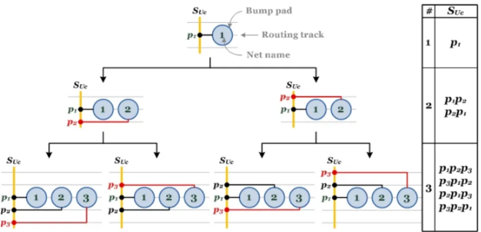
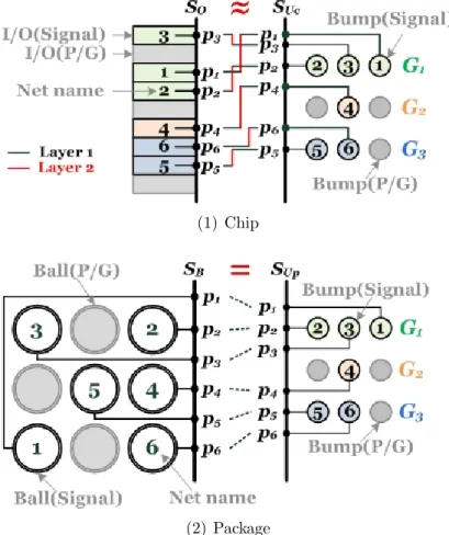
are consisted of three major domains marked with colors: bump as-signment, RDL routing, and substrate routing. Traditional flow costs more human resource and time because of the iteration. Proposed flow automatically solves the problem in a short time. . . 9
3.2 Four sequences, SO, SUC, SUP and SB, are built to specify
chip-package co-design problem. SO is the given I/O pin sequence. SUC
and SUP are two virtual pin tracks constructed by performing a
row-based projection technique on bump matrix on chip and package re-spectively. SB symbolizes the escape pin ordering from ball matrix.
In addition, SO ≃ SUC because we use channel routing algorithm to
solve RDL routing and SUP must be exactly the same as SB due to
the constraint of single-layer routing on package. Furthermore, to simultaneously achieve the two objectives mentioned in Chapter ??, we first group nets row by row in top-down order with notation G1,
G2, G3 and so on, then add this constraint into B-Escape routing
algorithm [2]. . . 10 3.3 Due to net grouping, there are two situations when reaching a
reorder-ing point of the reformation of B-Escape algorithm [2]: the chosen net
Ni and the next candidate net Nj are in the same group as shown
in (1) or not as shown in (2). The net cross caused by routing order exchange inside group could be solved by using different projection patterns of the bump row on chip and package. However, the net cross produced by routing order exchange between groups would never be solved since the projection method is row-based. Therefore, situation (1) has higher priority when backtracking. . . 14 3.4 An example that demonstrates the process of bump assignment. First
we derive all possible solutions of bump assignment based on ball escape routing result as shown in (1), then choose the candidate which projeccts the most similar bump pin sequence to I/O pin sequence as shown in (2). . . 16
3.5 Comparison between grid via and stagger via. As shown in (1), an assignment A′U consist of A1U′, A2U′ and A3U′ is illegal since there is no routing space for nets N3 and N7 while dropping vias over bumps.
However, (2) shows that A′U is a legal solution by staggering and compacting vias based on DRC rules. . . 17 3.6 Comparison between bump projection method in [1] and that in this
thesis. In (1), bumps can project in only one direction; therefore it might cause more overlaps. Hence, a bi-direction projection method is developed to reduce net crossing as shown in (2). . . 19 3.7 List of bump pin track. Since the connection between bump pads and
pins should be completed in single layer, the pin order can be derived as demonstrated. A new pin is located on either top or down of the original pin sequence. Thus, some particular patterns, for example,
SUC = p2p3p1, will never be generated. . . 20
3.8 An example for RDL routing. Given I/O pads and bump pads which are assigned, we first intuitively consider I/O pads as a pin track SO.
Then, we calculate the cost of each candidate for SUC. Finally, we
choose the pattern with minimum cost and perform classical channel routing algorithm. . . 20 4.1 A solution of bump assignment with single-layer substrate routing
simulation that generates by the reformation of B-Escape algorithm [2] in up-down mode. Green paths are the escape routing result of ball; fly-lines colored in blue indicate the assignment between bumps and balls. . . 22 4.2 Based on our bump assignment, we can achieve 100% routability in
RDL routing by [1] in case1. . . 24 ix
Chapter 1
Introduction
Figure 1.1: The cross section of flip-chip. In this work, the problem structure is from I/O pads through bump pads to solder balls.
Bump assignment plays an important role in chip and package designs. As illustrated in Fig. 1.1, flip-chip design consists of three domains: chip, package and board. In current industrial design flow, the designers first generate corresponding bump assignment based on experience according to the I/O sequence and the ball map given by customer, then perform RDL routing and substrate routing respec-tively. In addition, the assignment is composed of repeating pattern which satisfies power constraint but disregards routing information. It might consequently results in serious net congested problem on chip or package. Once the designers cannot find a legal routing solution, they have to reassign bumps then create chip and package layout all over again. Normally, this back and forth procedure has to be executed for many times, thus slowing down time to market and reducing the profits.
1.1
Previous Works
To improve the layout performance or to speed up design cycle, several previ-ous works proposed cross-domain co-design methodology in variprevi-ous aspects such as placement [4, 5], routing [6, 8, 9], assignment [10, 11, 12] and design flow [13, 14]. For chip-package co-design problem, [4] proposed a multi-step algorithm based upon integer linear programming to find an I/O placement solution satisfying all design constraints. [5] addressed a block and I/O buffer placement method that optimizes wire length and signal skew. Some researches [6, 8] developed RDL routers for area-I/O to achieve better performance. [9] fast generated an estimation of wire planning in package and board for chip and board designs awareness. Since bump and finger are the interface between chip and package, [10, 11, 12] focused on the pin assignment for increasing routability. Furthermore, the main reason that causes the bottleneck of co-design problem is the iteration of design process. Therefore, [13] provided a board-driven Λ-shaped co-design flow with true bi-directional infor-mation interactions and [14] offered a concurrent design flow to avoid much longer turn-around time.
However, the aforementioned previous works did not emphasize on substrate routing. Instead of physically connecting bumps and balls, some of them judge routability by fly-line or probabilistic prediction. Although the assignment pro-posed by [10] considers routability on package, it is suitable only for wire-bonding package. [13] proposed a two-pass flow to optimize pin assignment and pin routing simultaneously, yet the placement of I/O is not that flexible due to various design constraints. As a result, they might still meet design difficulties.
1.2
Our Contributions
In this thesis, we propose a fast heuristic in chip-package co-design in order to automatically obtain a bump assignment which introduces 100% routability both in RDL routing and substrate routing in our industrial case. Our approach also provides a practical RDL layout and a routing order that guides designers to easily finish net connection on package. Moreover, it can be used as a routing simulator as well. Since the results reflect the quality of initial I/O pin sequence and ball map, improper mapping can be fixed in the early stage for reducing design period and manual effort.
1.3
Thesis Organization
The remainder of this thesis is organized as follows. Chapter 2 introduces the framework of chip-package design problem. Chapter 3 discusses the proposed co-design flow then dilates on each stage. Chapter 4 reports our experimental results on one real industrial case. Finally, we conclude this thesis in Chapter 5.
Chapter 2
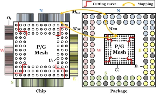
Problem Formulation
Figure 2.1: Top view of chip and package. The whole model is partitioned into four portions: west, north, east and south. First, the I/O pads are divided into four groups by locality. Then, the solder balls are distinguished according to the groups of their corresponding I/O pads. Finally, the bump pads are sliced into four sectors by cutting curves derived from two diagonals of chip.
Our chip-package co-design problem is to find a solution of bump assign-ment such that both RDL and substrate routing can meet the requireassign-ments without repeating the entire process over and over again. More specifically, we are given physical locations of peripheral I/O pads O, bump pads U , and solder balls B as illustrated in Fig. 2.1. Each I/O and ball are assigned to a specific net. The
ping between them is denoted by MOB. Our goal is to appropriately assign bumps
for the purpose of 100% routability in RDL routing and substrate routing under the corresponding I/O-bump mapping MOU and bump-ball mapping MU B. Note
that the mapping derived from MOU and MU B should be exactly the same as MOB.
Furthermore, since we use [1] which guarantees 100% routability to complete RDL routing, our objective in chip domain is to minimize the number of routing tracks instead.
Input:
i) Chip domain:
- Physical locations of each I/O pad Oi and each bump pad Ui on chip.
- Peripheral I/O pin sequence is given by designer. - Routable region: top two layers in this research. ii) Package domain:
- Physical locations of each bump pad Ui and each solder ball Bi on
pack-age.
- Solder ball map is given by designer.
- Routable region: single layer in this research.
iii) Design rules such as wire width, spacing constrain, size of Oi, Ui, Bi, and via.
Output:
i) A solution of bump assignment.
ii) Practical RDL routing result in pseudo single-layer [1]. iii) An illustration of planar substrate routing.
Objectives:
i) Chip domain: minimize the routing area borrowed from another existing metal layer (minimize number of tracks in channel routing) [1].
ii) Package domain: 100% routability.
In our implementation, the whole model is divided into four portions as shown in Fig. 2.1: west, north, east, and south by the following instructions. We first group I/O pads according to locality then distinguish their corresponding solder balls. The bump pads are partitioned by two diagonals of the chip and so does the routing area of RDL. Once solder balls and bump pads are sliced, four routing regions of package are generated. Here we transform coordinates into west coordinate system and consider west model only.
Chapter 3
Bump Assignment and Package
Planning
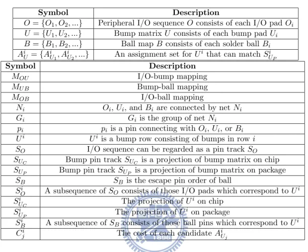
In this chapter, we first compare between traditional co-design flow and the pro-posed co-design flow in Section 3.1, then particularly describe each stage of our methodology in Section 3.2-3.5. Since planar routing is still required even though multiple routing layers are available for substrate routing due to signal integrity and manufacturability as mentioned in [3], the substrate routing problem can be transformed into escape routing problem. Therefore, we reform B-Escape routing algorithm proposed by [2] with net grouping technique (Section 3.2) to solve sub-strate routing (Section 3.3). Based on the escape routing order of ball and the I/O pin sequence, a solution of bump assignment can be generated (Section 3.4). Fi-nally, we complete RDL routing by applying the work in [1] (Section 3.5). All the notations is summarized in Table 3.1.
3.1
Design Flow
As shown in Fig. 3.1, the chip-package co-design problem consists of three major domains interacting with each other: bump assignment, RDL routing, and substrate routing. It is almost impossible to set compromising bump assignment between chip and package without any routing information. Therefore, designers first roughly
Table 3.1: Symbol Table
Symbol Description
O ={O1, O2, ...} Peripheral I/O sequence O consists of each I/O pad Oi
U ={U1, U2, ...} Bump matrix U consists of each bump pad Ui
B ={B1, B2, ...} Ball map B consists of each solder ball Bi
AiU ={AiU
1, A
i
U2, ...} An assignment set for U
i that can match Si UP
Symbol Description
MOU I/O-bump mapping
MU B Bump-ball mapping
MOB I/O-ball mapping
Ni Oi, Ui, and Bi are connected by net Ni
Gi Gi is the group of net Ni
pi pi is a pin connecting with Oi, Ui, or Bi
Ui Ui is a bump row consisting of bumps in row i
SO I/O sequence can be regarded as a pin track SO
SUC Bump pin track SUC is a projection of bump matrix on chip SUP Bump pin track SUP is a projection of bump matrix on package
SB SB is the escape pin order of ball
SOi A subsequence of SO consists of those I/O pads which correspond to Ui
SUi C The projection of U i on chip SUi P The projection of U i on package
SBi A subsequence of SB consists of those ball pins which correspond to Ui
Cji The cost of each candidate AiU
j
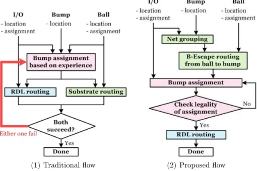
assign bumps based on experience and specific patterns. Then they will iteratively revise it depending on the routing results in the traditional design flow (as shown in Fig. 3.1(1)). In contrast, we propose a straightforward co-design flow to solve this problem by adjusting design order to be substrate routing, then bump assignment, and finally RDL routing, shown in Fig. 3.1(2).
Since the quality of an assignment is judged by routing results, we first detail our routing algorithm. For chip, we adopt [1] to solve congested RDL connection because of 100% routability and easy implementation. As shown in Fig. 3.2(1), it is intuitive to regard I/O pads as a pin track SO. Additionally, a row-based projection
is performed on bump matrix to build a virtual track SUC. Then we can apply
classical channel routing algorithm for pin connection. Note that SO does not have
to be identical with SUC due to two routing layers.
(1) Traditional flow (2) Proposed flow
Figure 3.1: The comparison between traditional flow and proposed flow. Both are consisted of three major domains marked with colors: bump assignment, RDL routing, and substrate routing. Traditional flow costs more human resource and time because of the iteration. Proposed flow automatically solves the problem in a short time.
For package, the routing area is decomposed into two parts: bump area and ball area. As shown in Fig. 3.2(2), SUP is obtained by the aforementioned
projection and will be similar to SUC. According to [3], substrate routing should be
planar although there are multiple available layers. Therefore, the concept of escape routing which is usually performed on PCB board can be imported. Here we choose [2] to form SB which must be exactly the same as SUP due to planar routing.
In conclusion, the ideal situation that concurrently achieves our two objec-tives mentioned in Chapter 2 occurs when SO≃ SUC ≃ SUP = SB. For this purpose,
we first divide nets into groups, which represents global assignment structure, depending on the given SO and the above projection method. SB will resemble SO
as much as possible by adding this information to the cost function of B-Escape algorithm [2]. In the end, we can determine the detailed bump assignment
(1) Chip
(2) Package
Figure 3.2: Four sequences, SO, SUC, SUP and SB, are built to specify chip-package
co-design problem. SO is the given I/O pin sequence. SUC and SUP are two virtual
pin tracks constructed by performing a row-based projection technique on bump matrix on chip and package respectively. SB symbolizes the escape pin ordering
from ball matrix. In addition, SO ≃ SUC because we use channel routing algorithm
to solve RDL routing and SUP must be exactly the same as SB due to the constraint
of single-layer routing on package. Furthermore, to simultaneously achieve the two objectives mentioned in Chapter 2, we first group nets row by row in top-down order with notation G1, G2, G3 and so on, then add this constraint into B-Escape routing
algorithm [2].
sections discuss the algorithm of each step.
3.2
Net Grouping
To simultaneously achieve high routability in both RDL routing and substrate routing, the escape routing order of ball should be similar to the given I/O pin sequence (SB ≃ SO) as discussed in last section. Since the original B-Escape routing
algorithm [2] considers only routability, we introduce the I/O information into it by net grouping technique.
Fig. 3.2 demonstrates the way how a bump pin track SUC or SUP is
con-structed on chip or package. Since the bump pin track is generated by the row-based projection method, we group bumps row by row in top-down order with notation
G1, G2, G3 and so on. To reduce routing tracks in RDL, SUC should be quite
simi-lar to the given SO. Consequently, each group is expected to be assigned with the
corresponding nets. As shown in Fig. 3.2(1), group G1 includes net N1, N2, and
N3, group G2 includes N4, and group G3 includes N5 and N6.
Net grouping symbolizes the idea of global bump assignment. If all the four pin tracks SO, SUC, SUP and SB are organized in the same group order, the routing
result is optimal. Furthermore, net grouping merely reveals the distribution, it does not specify the detailed assignment to each bump in row. In other words, SUC and
SUP are uncertainly equal to each other in spite of the same group order. This can be
seen in the following example: in Fig. 3.2(1), SUC = (p3p1p2)(p4)(p6p5) = G1G2G3;
in Fig. 3.2(2), SUP = (p1p2p3)(p4)(p5p6) = G1G2G3. In summary, net grouping
3.3
Substrate Routing
As mentioned previously, we separate the routing area of bumps and balls on package. In this section, we focus on ball area since we use coherent routing method for bumps on chip and package which will be discussed in Section 3.5. Considering signal integrity and manufacturability, substrate routing should be completed in single layer as described in [3]. For this reason, the connection from balls to SB
can be mapped into single-component escape routing problem even though it acts on PCB board. The entire ball area split into four components. Each of them has an individual escape boundary, that is, SB. In the next few paragraphs, we will describe
how to solve this problem by modifying cost function in B-Escape routing algorithm [2] with net grouping.
Algorithm 1 shows our reformation of B-Escape routing algorithm [2]. The overall process comprises three steps as original: Step1 is to calculate routing cost of each net (Line 2-Line 6); Step2 is to sort net costs(Line 7-Line 14); Step3 is to route the first net or backtrack(Line 15-Line 21). However, the routing cost is changed into 3-element vector (α, β, γ). For this reason, the details of the three steps differ from [2] and will be individually specified in the next three paragraphs.
Here α and β follow the definition in [2] which respectively stands for the number of unroutable balls and the number of blocked balls caused by current routing net. These two elements dominate the routability (Objective ii in Chapter 2). To optimize RDL routing (Objective i in Chapter 2), SO and SUC should be
alike. According to the relationship among the four sequences described in Section 3.1, SO ≃ SUC ≃ SUP = SB is derived. Hence we define the third element γ as the
group of net. By following the group order during escape routing, the escape order
SB will be similar to the given I/O pin sequence SO.
Net cost ordering depends on routing modes clarified in [2]. In upward mode, 12
Algorithm 1 Reformation of B-Escape routing algorithm
1: for each of the six routing mode do
2: for each unrouted net Ni do
3: route net Ni from ball Bi to escape boundary SB
4: calculate the cost vector for net Ni
5: clear the route generated for net Ni
6: end for
7: if upward mode then
8: sort all net costs by group in non-decreasing order
9: else
10: sort all net costs by group in non-increasing order
11: end if
12: for each group do
13: sort net costs by α and β in non-decreasing order
14: end for
15: choose the first net Nj
16: if net Nj traps other nets then
17: backtrack and reorder
18: else
19: route net Nj from ball Bj to escape boundary SB
20: remove net Nj from net cost order
21: end if
22: until all nets are routed or exceed the backtrack limit
23: store the solution for this routing mode
24: end for
25: output the solution with the best routability
a pin first goes straight up to the boundary then follows the boundary clockwise until it reaches SB. All unrouted pins will be located lower than the current pin on
SB. Consequently, the net clustered in top group should be routed earlier. Thus,
the net costs are arranged as {G1, G2, G3, ...}. During downward mode, it is in
reverse order {..., G3, G2, G1}. Moreover, cost ordering inside each group is in
non-decreasing order based on α and β.
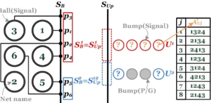
Since the costs are organized by net group in the reformation, there are two situations: (a) the chosen net Ni and the next candidate net Nj are in the same
group (Gi = Gj); (b) Niand Nj are in different groups (Gi ̸= Gj). Once all unrouted
(1) Reordering inside group (2) Reordering between groups
Figure 3.3: Due to net grouping, there are two situations when reaching a reordering point of the reformation of B-Escape algorithm [2]: the chosen net Ni and the next
candidate net Nj are in the same group as shown in (1) or not as shown in (2).
The net cross caused by routing order exchange inside group could be solved by using different projection patterns of the bump row on chip and package. However, the net cross produced by routing order exchange between groups would never be solved since the projection method is row-based. Therefore, situation (1) has higher priority when backtracking.
backtrack to route Nj first instead of Nias described in [2]. Situation (a): as shown in
Fig. 3.3(1), the exchange of routing order inside group does not influence the result of bump assignment. Therefore, it will not cause extra net crosses. Situation (b): the exchange of routing order between groups leads to the exchange of assignment between bump rows as shown in Fig. 3.3(2). As a result, net crosses are produced in RDL routing. Thus, situation (a) has higher priority when backtracking. According to aforementioned instructions, we can finally acquire an escape routing solution of balls whose SB is the most similar to SO with 100% routability.
3.4
Bump Assignment
Here we present three steps to determine an optimal solution of bump assignment by SOand SB. First, owing to single layer routing on package, SUP must be identical
to SB. For each bump row Ui, there is an assignment set AiU that can match the
corresponding segment SUiP by performing the projection method, detailed in the next section. Then, we derive the candidates for Si
UC from A
i
U in the same way.
In addition, cost Ci
j is defined as the differences between candidate SUiCj and S
i O.
Finally, we combine every Ai
U with minimum cost and verify it with design rules.
Fig. 3.4 demonstrates an example to clarify the process. As shown in Fig. 3.4(1), there are eight possible assignments A1
U1-A
1
U8 for bump row U
1 to form S1
UP =
p3p1p2p4. Fig. 3.4(2) illustrates the candidate SU1C1 projected from A
1
U1. Comparing
each S1
UCj and S
1
O, the cost Cj1 is the difference between the length of SO1 and the
length of the longest common sequence (LCS) of them. Note that the LCS represents the similarity. The assignment which has lowest cost is denoted by A1U′. Repeat all steps above until all AiU′ are found.
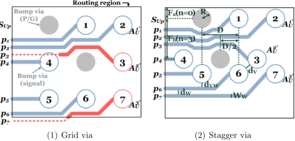
In this work, we verify the sufficiency of routing resource for the solution composed of AiU′ instead of physically routing bumps to SUP. On chip, the number
of tracks between two adjacent bump rows is large than the number of bumps in a row. On package, it is completely the opposite. To improve routability, designers will relocate bump vias by connecting short wires from bumps in previous layer rather than dropping vias over bumps. This method is quite similar to the flexible
via-staggering technique proposed in [3]. For example, given SUP = p1p2...p7 and
A′U = {A1′
U, A2
′
U, A3
′
U} as shown in Fig. 3.5(1). If the vias are located right on the
bumps, nets N3 and N7 will cause violation. It can be seen in Fig. 3.5(2) that A
′
U
(1) SUP is the same as SB due to single-layer substrate routing.
For bump row U1, there is an assignment set A1
U consisting of each candidate A1
Uj that produces corresponding projection S
1
UP.
(2) First, draw the corresponding subsequence S1Owhich is composed of net pins identical with that assigned to U1. For each candidate
A1Uj, perform the projection method with target SO1 to make the result S1
UCj as similar to S
1
O as possible. Then, calculate the cost C
1
j which is defined as the difference between the length of S1
O and the length of the longest common sequence (LCS) of S1
UCj and S
1
O.
Figure 3.4: An example that demonstrates the process of bump assignment. First we derive all possible solutions of bump assignment based on ball escape routing result as shown in (1), then choose the candidate which projeccts the most similar bump pin sequence to I/O pin sequence as shown in (2).
(1) Grid via (2) Stagger via
Figure 3.5: Comparison between grid via and stagger via. As shown in (1), an assignment A′U consist of A1′
U, A2
′
U and A3
′
U is illegal since there is no routing space
for nets N3 and N7 while dropping vias over bumps. However, (2) shows that A
′
U is
a legal solution by staggering and compacting vias based on DRC rules. The formulas (3.1) and (3.2) are specified below:
Fa(n) = { max(dv,dvw) 2 + R , n = 0 max(dw,dvw) 2 + nWw+ (n− 1)dw + dvw+ R , n ≥ 1 (3.1) Fb(n) = √ (2R + dv)2− (D2)2 , n = 0 √ (2R + 2dvw+ nWw+ (n− 1)dw)2− (D2)2 , n≥ 1 (3.2) Notations:
• n: the number of wires.
• D: the distance between two adjacent bump vias. • R: the radius of a bump via.
• dv: the minimum spacing between two adjacent vias.
• dw: the minimum spacing between two adjacent wires.
• dvw: the minimum spacing between a via and a wire.
Here we stagger and compact bump vias row by row from top to down. There are two cases: a via row is located between routing boundary and another via row; a via row is located between two via rows. Formula (3.1) is applied to the former and formula (3.2) is applied to the latter. It is evident to obtain the two formulas according to Pythagorean theorem. Note that the new location of a via can not be higher than the original location, or the two adjacent via rows will overlap. After the lowest row is compacted, the legality of an assignment A′U can be judged on whether the lowest row is located inside the routing region.
However, it is no guarantee of the existence of legal solution. Once A′U fails, we will analyse the bottleneck and update Ai′
U around it. If all combinations of A
′
U
can not meet the requirement, it concludes that the routing constraint is extremely tight. Thus, the only way to solve this problem is to stagger vias in manual or modify the given I/O pin sequence or ball map.
3.5
RDL Routing
After bump assignment, the methodology proposed in [1] is applied to solve RDL routing in pseudo single-layer. The problem is transformed into classical channel routing problem by considering I/O pads as a pin track SO and projecting bump
matrix to a virtual track SUC. As shown in Fig. 3.6(1), the projection in [1] is
executed in only one direction (downward). The inflexibility of bump pin order will cause extra overlaps. Hence, we refine it by offering two projective directions (upward and downward) as shown in Fig. 3.6(2). Please notes that both techniques are row-based.
Fig. 3.7 lists all patterns of bump pin order generated by our projection method. Due to the non-detour routing in single-layer, some particular patterns, for example, SUC = p2p3p1, are uncovered. The cost of each pattern is equal to the
(1) Original projection method in [1]
(2) Proposed projection method
Figure 3.6: Comparison between bump projection method in [1] and that in this thesis. In (1), bumps can project in only one direction; therefore it might cause more overlaps. Hence, a bi-direction projection method is developed to reduce net crossing as shown in (2).
difference between bump pin order and the corresponding I/O subsequence. It is similar to the definition of Ci
j described in Section 3.4. With the minimum cost
pattern, the usage of tracks will be reduced in RDL routing. The whole procedure is displayed in Fig. 3.8.
Figure 3.7: List of bump pin track. Since the connection between bump pads and pins should be completed in single layer, the pin order can be derived as demon-strated. A new pin is located on either top or down of the original pin sequence. Thus, some particular patterns, for example, SUC = p2p3p1, will never be generated.
Figure 3.8: An example for RDL routing. Given I/O pads and bump pads which are assigned, we first intuitively consider I/O pads as a pin track SO. Then, we
calculate the cost of each candidate for SUC. Finally, we choose the pattern with
minimum cost and perform classical channel routing algorithm.
Chapter 4
Experimental results
The proposed algorithms are performed on a real and large-scale industrial case. This case contains chip domain and package domain. As shown in Fig. 4.1 and Fig. 4.2, the distributions of I/Os, bumps, and balls in south and east regions are uniform; in west region, balls are distributed uniformly but bumps and I/Os are distributed in corner; in north region, all I/Os, bumps, and balls are distributed in corner.1 In this chapter, we first detail the execution flow, then compare the results
of substrate routing, bump assignment and RDL routing with that of traditional co-design flow.
4.1
Co-Design Flow
The whole methodology can be divided into three parts: (a) substrate routing in Section 3.2-3.3, (b) bump assignment in Section 3.4 and (c) RDL routing in Section 3.5. (a) and (b) are implemented in C++; (c) is implemented in tool command language Tcl. First, the data are fetched from the chip design in Encounter Digital Implementation (EDI) and the package design in Cadence Allegro. Then, a sub-strate routing order considering RDL routability with the corresponding simulation
1The combination of various types of distribution in different design domain increases the
rout-ing difficulty. For example, in west region, EDI router can only complete less than half of nets in RDL routing.
of single-layer substrate routing is generated by (a). After bump assignment, (c) connects I/O and bumps in pseudo single-layer and dumps scripts of commands in few minutes. Finally, the physical RDL layout will be obtained by sourcing these scripts in EDI.
4.2
Substrate Routability
Figure 4.1: A solution of bump assignment with single-layer substrate routing simu-lation that generates by the reformation of B-Escape algorithm [2] in up-down mode. Green paths are the escape routing result of ball; fly-lines colored in blue indicate the assignment between bumps and balls.
Fig. 4.1 shows our results of bump assignment and substrate routing in a real industrial case with 507 signal nets (case1). Since we perform the reformation of B-Escape routing algorithm [2] on uniform grid, the routing paths produce 90 degree
corner and cost more routing resource than 45 degree router. Therefore, it can be treated as the lower bound of routing performance. By following the escape order, designers can easily complete the physical substrate routing with 100% routability in Cadence Allegro. Although Allegro offers automatic router for package, designers still connect each bump and ball in manual because of the poor routability (40%-50%) and redundant detours.
4.3
Bump Assignment
Table 4.1: The comparison of chip-package co-design flow in case1. Method Substrate routing
# routed nets Rout. Time Ours 507/507 in 2nd layer 100% 909.52 (sec.)
Traditional 449/507 in 2nd layer 100% a few days 58/507 in 3rd layer
Method RDL routing
# routed nets Rout. Time Ours 507/507 in pseudo single-layer 100% < 1 minute
Traditional 507/507 in two layers 100% > 2 weeks
As shown in Table 4.1, the substrate routing results reflect the quality of assignment method. By using the technique of via staggering mentioned in Section 3.4 during bump assignment, our co-design flow can achieve planar substrate routing. In contrast, designers assign bumps based on experience and iteratively revise the solution in traditional flow. Therefore, it requires more routing resource and more time to finish all connections.
4.4
RDL Routability
Fig. 4.2 shows the result of RDL routing by obtained [1] under our bump assign-ment. We first dump the assignment in script of command then source it in EDI
Figure 4.2: Based on our bump assignment, we can achieve 100% routability in RDL routing by [1] in case1.
routing area borrowed from another existing layer is quite equal to that of manual. Both flow produce 100% routability RDL routing, but our flow is much faster than the traditional co-design flow.
Chapter 5
Conclusions
In this thesis, we propose a straightforward chip-package co-design flow with routability-driven bump assignment based on [1] and [2]. By considering I/O pin sequence as a target order for ball escape routing, a compromise of bump assignment between chip and package can be generated. This technique offers information interactions to avoid the iterative revise in traditional design flow. The experimental results have shown that our approach achieves 100% routability in both RDL routing and substrate routing. In addition, since the whole process is automatic, it is much faster than the traditional design flow.
Bibliography
[1] H. W. Hsu, M. L. Chen, H. M. Chen, H. C. Li, and S. H. Chen, “On effective flip-chip routing via pseudo single redistribution layer,” in Proc. of Design,
Automation and Test in Europe Conference and Exhibition, pp. 1597–1602,
2012.
[2] L. Luo, T. Yan, Q. Ma, M. D. F. Wong, and T. Shibuya, “B-escape: a simultaneous escape routing algorithm based on boundary routing,” in Proc.
of International Symposium on Physical Design, pp. 19-25, 2010.
[3] S. Liu, G. Chen, T. T. Jing, L. He, T. Zhang, R. Dutta, and X. L. Hong, “Substrate topological routing for high-density packages,” in IEEE Trans.
on Computer-Aided Design of Integrated Circuits and Systems, vol. 28, no.
2, pp. 207-216, Feb. 2009.
[4] J. Xiong, Y. C. Wong, E. Sarto, and L. He, “Constraint driven I/O plan-ning and placement for chip-package co-design,” in Proc. of Asia and South
Pacific Design Automation Conference, pp. 207-212, 2006.
[5] M. F. Lai and H. M. Chen, “An implementation of performance-driven block and I/O placement for chip-package codesign,” in Proc. of International
Symposium on Quality Electronic Design, pp. 604-607, 2008.
[6] K. S. Lin, H. W. Hsu, R. J. Lee, and H. M. Chen, “Area-I/O RDL routing for chip-package codesign considering regional assignment,” in Proc. of IEEE
Electrical Design of Advanced Packaging and Systems Symposium, pp. 1-4,
2010.
[7] J. W. Fang and Y. W. Chang, “Area-I/O flip-chip routing for chip-package co-design,” in Proc. of IEEE/ACM International Conference on
Computer-Aided Design, pp. 518-522, 2008.
[8] J. W. Fang and Y. W. Chang, “Area-I/O flip-chip routing for chip-package co-design considering signal skews,” in IEEE Trans. on Computer-Aided
Design of Integrated Circuits and Systems, vol. 29, no. 5, pp. 711-721, 2010.
[9] R. J. Lee, H. W. Hsu, and H. M. Chen, “Board- and chip-aware package wire planning,” in IEEE Trans. on Very Large Scale Integration Systems, Sept. 2012.
[10] C. H. Lu, H. M. Chen, C. N. J. Liu, and W. Y. Shih, “Package routability-and IR-drop-aware finger/pad assignment in chip-package co-design” in Proc.
of Design, Automation and Test in Europe Conference and Exhibition, pp.
845-850, 2009.
[11] H. Han, W. Yin, W. Wang, and Z. Pang, “Auto-assign method for large scale flip-chip package design,” in Proc. of IEEE International Conference
on ASIC (ASICON), pp. 929-932, 2011.
[12] T. Meister, J. Lienig, and G. Thomke, “Interface optimization for improved routability in chip-package-board co-design,” in Proc. of International
Work-shop on System Level Interconnect Prediction, pp. 1-8, 2011.
[13] H. C. Lee and Y. W. Chang, “A chip-package-board co-design methodology,” in Proc. of ACM/IEEE Design Automation Conference, pp. 1082-1087, 2012.
[14] R. J. Lee and H. M. Chen, “A study of row-based area-array I/O design planning in concurrent chip-package design flow,” in Proc. of ACM Trans.
on Design Automation of Electronic Systems, vol. 18, no. 2, pp. 1-19, 2013.

![Figure 3.3: Due to net grouping, there are two situations when reaching a reordering point of the reformation of B-Escape algorithm [2]: the chosen net N i and the next candidate net N j are in the same group as shown in (1) or not as shown in (2).](https://thumb-ap.123doks.com/thumbv2/9libinfo/8653974.194217/26.892.198.698.150.503/figure-grouping-situations-reaching-reordering-reformation-algorithm-candidate.webp)
![Figure 3.6: Comparison between bump projection method in [1] and that in this thesis. In (1), bumps can project in only one direction; therefore it might cause more overlaps](https://thumb-ap.123doks.com/thumbv2/9libinfo/8653974.194217/31.892.240.653.157.485/figure-comparison-projection-method-thesis-project-direction-overlaps.webp)