dTaiwan Semiconductor Manufacturing Co., Ltd., Hsinchu 300, Taiwan
Received 11 August 1998; received in revised form 6 January 1999; accepted 6 January 1999
Abstract
A multilayer thin ®lm structure (SiO2/SiNx/SiO2) with a one-step chemical±mechanical polish (CMP) process is developed for shallow trench ®lling and planarization for ULSI devices in the quarter micron regime. By ®ne-tuning the plasma-enhanced chemical vapor deposition (PECVD) conditions we successfully modi®ed the stoichiometry and other characteristics of the as-deposited SiNxand oxide ®lms. As these ®lm characteristics are changed, the CMP removal rate selectivity between sacri®cial oxide and nitride stopper layer can also be adjusted. Correspondingly, the CMP process latitude for shallow trench isolation in 0.25 mm memory devices can be broadened by sequentially depositing multilayered oxide and nitride ®lms with adjustable characteristics and CMP removal rates. Dishing-free wide trench areas with excellent planarity can be achieved through the integration of the proposed multilayered PECVD oxide/nitride scheme and the one-step CMP process. q 1999 Elsevier Science S.A. All rights reserved.
Keywords: Multilayer thin ®lm; Chemical±mechanical polish; Dielectrics; Shallow trench isolation; Silicon local oxidation
1. Introduction
For a long time, local oxidation of Si (LOCOS) was the standard technology to provide electrical isolation between active devices for integrated circuits (IC). As demands for smaller geometry and higher circuit density become stron-ger, even more stringent requirements are being placed upon the isolation performance, and problems with LOCOS begin to surface. For example, the lateral encroachment of ®eld oxide into device active areas and the poor planarity set the limitations for the utilization of this technology beyond 0.25 mm generation. In light of these limitations, an alternative process called shallow trench isolation (STI) has been pursued actively by IC manufacturers as the substitute to LOCOS for device isolation [1]. STI allows for higher chip density and thus promotes more ef®cient use of Si wafers. A typical STI process involves etching a trench pattern through a nitride layer, a thin pad oxide layer, and into the silicon. Subsequently, a chemical vapor deposited (CVD) oxide is laid on the entire wafer, ®lling into the trench area and overlying the nitride-protective active region. A chemical±mechanical polish (CMP) step follows then to
planarize the topography from previous deposition processes and stops ®nally on the nitride layer. The remain-ing nitride is removed subsequently by wet chemistry or reactive ion etching (RIE). The planarization issue is perceived as the most critical step to the success of STI [2,3]. Speci®cally, due to pattern density effects, nitride thickness after CMP can vary, creating step height variation and, in some cases, promoting overpolish of nitride layer, leading to deleterious damage of the active region. Along with the overpolish and pattern density issues is the dishing into the oxide-®lled trench region that may degrade the isolation performance. Extensive efforts have been invested to resolve these problems. These include adjustments in thickness of trench-®ll layer [2] and its characteristics (e.g., Poly-Si, HDP-CVD, SOG, etc.) [3,4], modifying slurry chemistries to achieve high oxide/nitride polish selec-tivity [5,6], implementation of a post-CMP RIE step to assist planarization [7,8], and layering the trench oxide with an additional nitride [9].
From a process integration point of view, a feasible and manufacturable STI process should take into account simul-taneously the thickness, characteristics and CMP perfor-mances of trench-®ll layer and nitride stop layer, so as to optimize the process latitude while minimizing overpolish
0040-6090/99/$ - see front matter q 1999 Elsevier Science S.A. All rights reserved. PII: S0040-6090(99)00028-0
and dishing. In addition, to reduce process complexity, use of an additional stop or sacri®cial layer or an extra RIE step to help achieve planarity should be avoided. Based on the perspectives above, in this investigation, we modify the stoichiometry and other characteristics of the plasma-enhanced chemical vapor deposition (PECVD) SiNx stop
layer and oxide trench ®ll layer, in order to optimize and improve the CMP process performances such as planarity, dishing, selectivity. Such modi®cations in thin ®lm charac-teristics would help enhance the throughput of CMP process itself for the implementation of shallow trench isolation into 0.25 mm device manufacturing.
2. Experimental
In this study, the multilayer thin ®lm structure for the STI process is manufactured by the combination of various thin ®lm deposition/growth techniques. The process sequence is summarized as follows:
1. PECVD nitride stacks (nitride 1 and nitride 2) are grown on 150 mm Si wafers as the polish stopping layers. The NH3/SiH4gas ¯ow rate ratio is adjusted to modify nitride
®lm properties. The thickness of the nitride stacks is varied to evaluate the CMP process latitude.
2. I-line lithography and trench etch.
3. Sidewall oxidation is performed to grow a thin oxide liner to protect the active region from subsequent proces-sing and to achieve better process control and device performance.
4. Bilayer subatmospheric chemical vapor deposited (SACVD) oxides are ®lled into the 450 nm deep trench
at 4008C with TEOS (tetraethoxysilane)/O3(ozone) gas
mixtures. The ozone concentration is adjusted so that a low-ozone oxide (100 nm) and a high-ozone oxide (500 nm) can be deposited subsequently.
5. Dual-frequency PECVD TEOS oxides are deposited as CMP sacri®cial layers. In this process, the N2O gas ¯ow
rate is maintained at 4.8 l/min, while the ¯ow rate of TEOS gas and low/high-frequency power ratio are both varied to modify the stoichiometry and characteristics of the deposited oxides. The TEOS/N2O gas ¯ow ratio is
increased from TEOS1 to TEOS5, representing different oxide ®lm characteristics. The cross-sectional view of the entire thin ®lm structure is shown in Fig. 1.
CMP experiments were carried out in an IPEC 472 Avanti polisher with IC1000/Suba IV pad and SC-112 slurry. The down force, back pressure, platen rpm, and carrier rpm used were maintained at 7 psi, 2 psi, 30 rpm and 20 rpm, respec-tively.
After ®lm deposition and CMP, physical and chemical characterization was performed. Standard wafer curvature measurement was used to determine the ®lm stress based on Stoney's equation. Fourier transform infrared (FTIR) spec-troscopy was employed to determine the bonding nature of the oxide and nitride ®lms. Wet chemical etching rate was determined using 10:1 buffered oxide etchant (BOE). CMP
Fig. 1. Cross-sectional view of the multilayer thin ®lm structure for shal-low-trench-isolation process.
Table 1
PECVD TEOS oxide characteristics
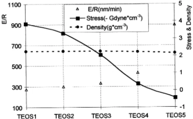
TEOS TEOS1 TEOS2 TEOS3 TEOS4 TEOS5 Stress (MPa) 386 330 205 38 244 Density (g/cm3) 2.27 2.27 2.26 2.23 2.16
R/R (nm/min) 185.6 218.7 245.6 261.7 333.1 E/R (nm/min) 273.3 301.1 332.1 433.9 898.9
Fig. 2. Effects of TEOS/N2O gas ¯ow ratio on ®lm stress, NH4F-buffered
HF chemical wet etch rate and ®lm density of oxides.
Fig. 3. Correlation between the wet etch rate and CMP removal rate of PE-TEOS oxide.
removal rate (CMP R/R) was calculated from difference in ®lm thickness measured at 49 points across the wafer. 3. Results and discussion
Table 1 summarizes the experimental results of PECVD TEOS oxide characteristics and their CMP results. These data are reproduced in Fig. 2, which shows that as the TEOS/N2O gas ¯ow ratio increases from TEOS1 to
TEOS5, the as-deposited ®lm stress changes from high tensile to low compressive, while the ®lm density decreases slightly. This decrease in tensile stress is accompanied by the increase in NH4F-buffered HF wet etch rate. Such an
increase in wet etch rate also correlates well with the rise in CMP polish rate, as shown in Fig. 3.
However, the above ®ndings seem contradictory to the work by Osenbach and Knolle [10]. They postulated that the presence of tensile stress in the silica structure would increase the electrochemical potential and hence chemical wet etch rate of the oxide ®lm, when the ®lm is immersed into the corrosive aqueous media. Another study [11] pointed out that the water diffusion rate in silica glass is a function of local stress. In that study, it was found that a
results in a more open structure in the oxide. Meanwhile, the hydrophilicity of the oxide is enhanced due to the formation of Si±OH bonds. Both of the scenarios above, i.e. reduction in ®lm density and enhancement in hydrophilicity, will enlarge the contact area and hence accelerate wet etch and polish rates, as found in the current study.
The correlation between hydrogen bonding concentration in PECVD silicon nitride ®lms and their respective ®lm density is exhibited in Fig. 4. As shown, both the numbers of Si±H and N±H bonds change the ®lm density signi®-cantly. The results are somewhat similar to previous studies on PECVD SiNx®lms [13,14]. It has been reported that a
higher Si±H/N±H bond density ratio corresponds to a lower SiNx®lm density and higher chemical etch rate in aqueous
¯uoride or chloride media [5,6]. Therefore, it can be postu-lated that the existence of more Si±H bonds increases the porosity of the PECVD SiNx, leading to increases in both the
chemical etch rate and the CMP removal rate. Increasing the porosity of the dielectrics also increases the speci®c area immersed in the slurry during CMP process. During the polishing process, the large speci®c area on the surface will provide larger area for the abrasives in the slurry to scrub the weakly bonded and porous SiNx ®lm. All of
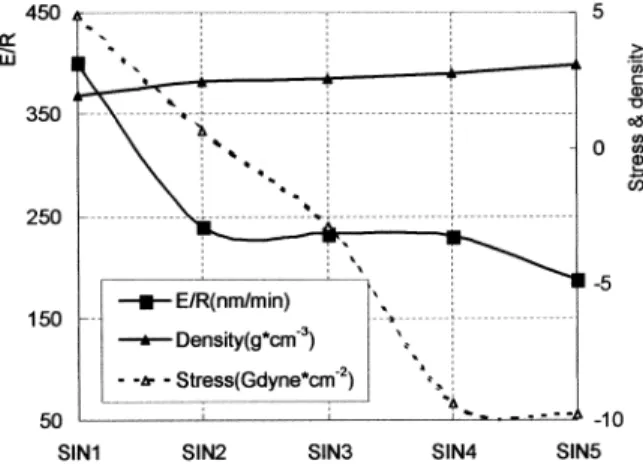
these effects contribute to the enhancement in chemical wet etch rate and CMP polish rate dramatically as shown in Figs. 5 and 6. Table 2 summarizes the material character-istics of PECVD silicon nitride and their respective CMP polish rates. Further improvement in CMP performance can be realized by modifying the stoichiometry of the intermedi-ate nitride stopping layer. This is achieved by modifying bias power while reducing SiH4/NH3gas ¯ow ratio during
deposition of PECVD nitride ®lms. The FTIR spectrum shows that the resulting PECVD nitride ®lms have different Si±H content. Concurrently, these as-deposited nitrides exhibit different BOE wet etch rates and compressive stres-ses, suggesting a signi®cant change in nitride ®lm structure and hence different CMP removal rates. With these changes in ®lm characteristics, a multilayer PECVD SiNx ®lm
deposition process is implemented with the intention to induce high/low CMP removal rates. The process goals are to completely remove the remaining oxide on nitride stop layer, and to prevent CMP dishing effect resulting from over polish. This point will be elaborated later.
To incorporate the above oxide/nitride thin ®lm stacks into the STI process, the thickness and deposition conditions are adjusted in order to broaden the process latitude while
Fig. 4. Effects of hydrogen-related bond in PECVD silicon nitride ®lms on ®lm density.
Fig. 5. Effects of stress and ®lm density on chemical wet etch rate of PECVD nitride thin ®lms.
minimizing dishing effects during polishing. A 200-nm thick nitride layer was deposited ®rst on the Si wafer. A 600-nm thick SACVD oxide was then ®lled into the 450-nm deep trench, whose width varies from 300 450-nm to 2000 nm. Subsequently, PECVD TEOS oxide layers of varying thickness were deposited and their CMP planarization performances were evaluated in order to optimize the process latitude.
For optimal planarization results, a 400-nm thick TEOS5 (CMP R=R 333 nm/min) was deposited ®rst followed by a 200-nm TEOS1 (CMP R=R 186 nm/min). The nitride polish stop layers were formed by sequentially depositing a SIN1 (nitride 1, CMP R=R 212 nm/min) layer of 130-nm thick followed by a SIN5 layer (nitride 2, CMP R=R 80 nm/min). Such a oxide/nitride combination with high/ low polish rates effectively enhances the throughput for the STI process. Initially, a TEOS5 oxide layer with a high R/R was adopted for bulk removal. The removal rate was reduced then by inserting a TEOS1 layer underneath, as the polish proceeds towards the oxide/nitride interface. Such a deceleration of polishing action effectively reduces the risk of overpolish and brings the dishing effect, if any, to a controllable extent. A nitride with a slightly higher removal rate (SIN1) than TEOS1 was utilized as the top polish stop layer (i.e. nitride 1) in order to compensate the drop in TEOS1 oxide removal rate due to the existence of the nitride substrate. Such a substrate effect [15] results when the vertical displacement during polishing is reduced as the abrasives indent into a ®lm on top of a mechanically harder substrate. The removal rate (R/R) can then be expressed as a function of Young's modulus, the applied pressure, and relative velocity:
R=R k 1=Ep1 1=Eu £ P £ V 1
where k is a parameter related to slurry concentration and chemical erosion effects; Epand Euare the Young's moduli
of the ®lm being polished and the underlying ®lm (substrate); P is the applied down pressure; and V is the relative velocity. The PE-TEOS oxide directly above the
harder nitride layer would exhibit a lower removal rate due to this substrate effect, while that above the trench area would polish at the same rate. Therefore, to maintain a planarized surface, the top nitride layer should be removed at a slightly higher rate than the TEOS1 layer, in order to compensate the dishing into the trench area. Finally, the
Fig. 6. Effects of chemical wet etch rate and ®lm density on CMP removal rate of PECVD nitrides.
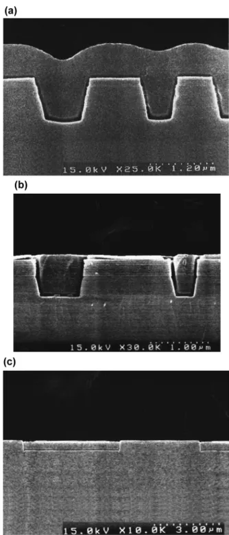
Fig. 7. (a) The multilayer STI structure before CMP and TEOS oxide deposition. (b) STI structure during an intermediate stage of CMP showing nitride remaining on the active region. The SEM sample is decorated to reveal the trench region. (c) The multilayered STI structure after CMP. Global planarization and minimum amount of dishing are achieved for wide trench patterns.
nitride with the lowest removal rate (SIN5) was laid under-neath as nitride 2 to effectively stop the polish action at the interface. At this time, all the PECVD TEOS oxide layer was removed, exposing the underlying SACVD trench oxide and the residual SIN5 layer, which was removed subsequently by wet H3PO4dip.
The above ®ndings serve as useful guidelines to design a multilayer PECVD oxide/nitride dielectric scheme for shal-low trench isolation process. Speci®cally, by introducing oxide/nitride layers with tunable CMP polish rates, the CMP dishing effect can be minimized easily without any modi®cation in slurry chemistry [8] or the implementation of complicated two-step polishing processes [9]. Another advantage of the current process is that the CVD and CMP throughput and process latitude can be expanded simultaneously. Fig. 7a is a SEM micrograph showing the cross-sectional view of a typical thin ®lm structure for STI before CMP. Trenches with different widths can be seen clearly. The STI structure during an intermediate CMP stage is exhibited in Fig. 7b. The SACVD low-ozone oxide was removed to decorate the trench. As shown in the picture, there is some residual nitride remaining on the active region. The ®nal STI structure after CMP is displayed in Fig. 7c. As the picture shows, a wide (4.5 mm) trench with a fully planarized surface is attained and the STI structure is delineated successfully by the CVD/CMP process scheme proposed in this study.
4. Conclusion
By modifying the PECVD deposition conditions we can manipulate the stoichiometry and other characteristics of the as-deposited SiNx and oxide ®lms for application in the
shallow trench isolation process. The CMP removal rates of the PECVD ®lms are ®ne-tuned and a multilayer thin ®lm stack is proposed in order to allow for a one-step CMP process for the de®nition of the shallow trench patterns. The implementation of the this multilayer PECVD dielectric process leads to enhancements in the CMP remove rate
selectivity and the ef®ciency of polish stop layer. The inte-gration of the proposed CVD and CMP processes produces a STI structure with a well-planarized surface and minimum amount of dishing.
Acknowledgements
Thanks are due to the kind support from thin ®lm module in Winbond Electronics Corp., for the wafer process. This project is supported in part by the National Science Council of Taiwan under contract No. 88-2216-E-009-015.
References
[1] P.C. Fazan, V.K. Mathews, Int. Electron Device Meeting (IEDM) Digest, IEEE, New York, 1993, p. 157.
[2] S.S. Cooperman, A.I. Nasr, G.J. Grula, J. Electrochem. Soc. 142 (1995) 3180.
[3] I. Ali, M. Rodder, S.R. Roy, G. Shinn, M.I. Raja, J. Electrochem. Soc. 142 (1995) 3088.
[4] S. Nag, A. Chatterjee, Solid State Technol. 40 (9) (1997) 129. [5] C.R. Mills, G.S. Grover, B.L. Mueller, J.S. Steckenrider, S.
Ganesh-kumar, G.W. Leach, C.K. Huang, J. Grillaert, Proc. 2nd CMP for USLI Multilevel Interconnection Conf., CMP-MIC, Tampa, FL, 1997, p. 179.
[6] T. Detzel, S. Hosali, A. Sethuraman, J.-F. Wang, L. Cook, J. Grillaert, Proc. 2nd Int. CMP for ULSI Multilevel Interconnection Conf., CMP-MIC, Tampa, FL, USA, 1997, p. 202.
[7] K. Smekalin, Solid State Technol. 40 (7) (1997) 187.
[8] J.-Y. Cheng, T.F. Lei, T.S. Chao, D.L.W. Yen, B.J. Jin, C.J. Lin, J. Electrochem. Soc. 144 (1997) 315.
[9] J.M. Boyd, J.P. Ellul, J. Electrochem. Soc. 143 (1996) 3718. [10] J.W. Osenbach, W.R. Knolle, J. Electrochem. Soc. 139 (1992) 3346. [11] M. Nogami, M. Tomozawa, J. Am. Ceram. Soc. 67 (1984) 151. [12] Y.-L. Wang, W.-T. Tseng, M.-S. Feng, Jpn. J. Appl. Phys. 36A (1997)
5492.
[13] I. Kobayashi, T. Ogawa, S. Hotta, Jpn. J. Appl. Phys. 2A (1992) 336. [14] B.T. Dai, W.F. Wu, C.H. Liu, C.W. Liu, C.F. Yeh, Proc. 12th VSLI Multilevel Interconnection Conf., CMP-MIC, Tampa, FL, 1995, p. 485.
[15] Y.-L. Wang, C. Liu, M.-S. Feng, J. Dun, K.-S. Chou, Thin Solid Films 308±309 (1997) 543.