INTRODUCTION
For the bonding of recycled sputtering targets to copper backing plates, soldering has been commonly employed as a low-temperature joining method. Pure indium is a popular solder for this application due to its lower melting point, greater ductility, and longer thermal fatigue life.1–3During the soldering process, intermetallic compounds form at the sol-der/substrate interface, which is assessed to be a sign of good connection in the solder joints. However, an overgrowth of intermetallic compounds will re-sult in brittle fracture at the interface. It also in-creases the difficulty in further recycling of the costly indium solder material.
The interfacial reactions between Cu and In have been reported in the literature. Vianco et al. studied the intermetallic compounds formed during the solid-state reaction in a Cu/In diffusion couple.4At an annealing temperature of 70°C, a metastable composition of Cu9In16was observed at the interface and subsequently turned into a dual-layer structure of Cu9In16 joined by an intermetallic compound, Cu11In9, at 100°C. At 135°C, it transforms into Cu11In9. The growth of the intermetallic compound was diffusion-controlled, and its apparent activation
energy was 20 kJ/mol. In the temperature range be-tween 100°C and 150°C, Manna et al. found the for-mation of Cu11In9 at the interface between an In thin film and a Cu single crystal.5The growth of the intermetallic compound also followed a parabolic re-lationship with an apparent activation energy of 26 kJ/mol.
With respect to the soldering reaction between liquid In and a Cu substrate, Kao dipped Cu disks into In and In ⫹ Cu baths at 200°C.6 Cu
11In9 was identified at the interface after both reactions. Su et al. found that the resulted intermetallic compound was Cu11In9by heating the Cu/In couple at 300°C.7 With respect to the Cu/In thin film reactions, rapid formation of the CuIn intermetallic com-pound was observed by Roy8 and Chen.9 They found that the CuIn intermetallic compound forms even at room temperature. However, the CuIn phase was not shown on the Cu-In phase diagram. Roy et al. investigated Cu/In thin film reactions by measuring the change of electrical resistance with time, where the growth of CuIn was confirmed by x-ray diffraction and transmission electron mi-croscopy. Chen et al. developed a 200°C fluxless process to produce Cu-In joints and discovered that CuIn intermetallic compounds were formed immediately after depositions of Cu and In thin films.
Intermetallic Compounds Formed at the Interface between
Liquid Indium and Copper Substrates
C.L. YU, S.S. WANG, and T.H. CHUANG
Institute of Materials Science and Engineering, National Taiwan University, Taipei 106, Taiwan, Republic of China.
The interfacial reactions between liquid In and Cu substrates at temperatures ranging from 175°C to 400°C are investigated for the applications in bonding recycled sputtering targets to their backing plates. Experimental results show that a scallop-shaped Cu16In9intermetallic compound is found at the Cu/In in-terface after solder reactions at temperatures above 300°C. A double-layer structure of intermetallic compounds containing scallop-shaped Cu11In9and continuous CuIn is observed after the Cu/In interfacial reaction at tempera-tures below 300°C. The growth of all these intermetallic compounds follows the parabolic law, which implies that the growth is diffusion-controlled. The acti-vation energies for the growth of Cu16In9, Cu11In9, and CuIn intermetallic compounds calculated from the Arrhenius plot of growth reaction constants are 59.5, 16.9, and 23.5 kJ/mole, respectively.
Key words: Cu/In interface, soldering reaction, intermetallic compound
(Received August 10, 2001; accepted January 16, 2002) 488
The efforts of this study are concerned with the identification of intermetallic compounds formed at the Cu/In interface after solder reactions in a wide temperature range between 175°C and 400°C. For this purpose, the morphology and growth kinetics of the intermetallic compounds are investigated. Their composition distributions
are also analyzed by electron probe microanalysis (EPMA).
EXPERIMENTAL
High-purity Cu substrates (99.95%) were cut to the size of 8 mm ⫻ 6 mm with a thickness of 0.8 mm. They were ground with 1500 mesh SiC paper and polished
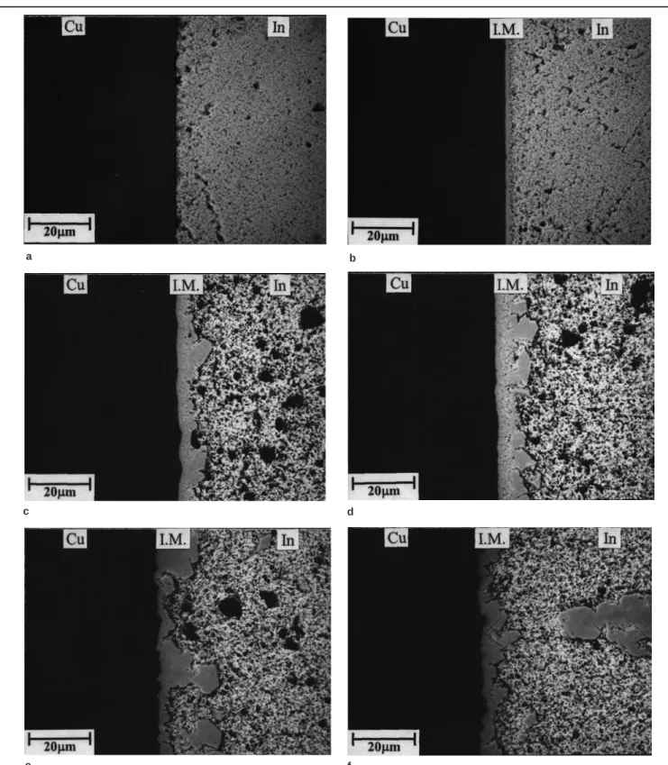
a b
c d
e f
Fig. 1. Microstructures of intermetallic compounds after Cu/In interfacial reactions at various temperatures for 15 min: (a) 175°C, (b) 200°C, (c) 250°C, (d) 300°C, (e) 350°C, and (f) 400°C.
Fig. 2. Micrograph of the intermetallic compound formed at the Cu/In interface after soldering reaction at 250°C for 120 min with the In solder selectively etched.
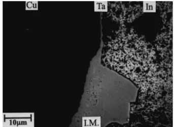
Fig. 3. Formation of different intermetallic compounds on both sides of the Cu/In interface marked with Ta thin film after soldering reaction at 250°C for 120 min.
with 0.3 m Al2O3 powder. The indium solder was rolled from an In ingot (99.99% purity) into a 0.3-mm-thick foil, and then cut to a size of 7 mm ⫻ 5 mm. A rosin mildly actived (RMA) type flux was lightly pasted over the Cu substrates, and the In foils were laid on the Cu substrates in an infrared furnace under vacuum of 10⫺3torr. Interfacial reactions were carried out at various temperatures ranging from 175°C to 400°C for various times.
For scanning electron microscopy morphology ob-servations, the reacted specimens were cut along the cross section, ground with SiC paper, and polished with 0.3 m Al2O3powder. A solution of 10 mL HF, 10 mL H2O2, and 40 mL H2O was used to selectively etch out In to reveal the intermetallic compounds. The compositions of intermetallic compounds were analyzed by EPMA. For clarifying the growth mech-anism of intermetallic compounds during the inter-facial reaction, the Cu substrate was partially sput-ter-coated with a Ta thin film that acted as a diffusion marker of the original Cu/In interface.
RESULTS AND DISCUSSION
Figure 1 shows the microstructure of intermetal-lic compounds (IMs) formed at the Cu/In interface after soldering reactions at various temperatures for 15 min. A single layer of the scallop-shaped in-termetallic compound appeared at the Cu/In inter-face after soldering as the temperature exceeds 300°C. Reactions at lower temperatures (below 300°C) result in a double interfacial layer consisting of both continuous and scallop-shaped intermetallic compounds. Such a bilayer of intermetallic com-pounds is further examined by selective etching of the In solder after interfacial reaction. The result in Fig. 2 indicates that the scallop-shaped intermetal-lic compound possesses a crystallographic structure, while the continuous layer of the intermetallic com-pound has a spherical structure. When the copper substrate is partially sputter-coated with a Ta thin film (which acts as a diffusion barrier between Cu and liquid In), the original Cu/In interface can be
marked. Figure 3 indicates that the Ta marker is lo-cated right on the line of demarcation between both intermetallic compounds in the double layer. With an increase in reaction time, both intermetallic com-pounds in the double layer will grow in opposite di-rections, as shown in Fig. 4. The EPMA analyses of the intermetallic compound formed at higher tem-peratures show a constant distribution with the stoi-chiometric composition of Cu16In9.
A typical result obtained from the specimens re-acted at 400°C for 120 min is shown in Fig. 5. The bi-layered intermetallic compounds formed in the speci-mens after soldering reactions at lower temperatures are also analyzed. Figure 6 shows that the scallop-shaped intermetallic compound possesses a constant Cu content of 55 at.%, which implies a stoichiometric composition of Cu11In9. Chemical analyses of the con-tinuous intermetallic layer reveal an average compo-sition of CuIn. However, the copper content of such a CuIn intermetallic compound declines slightly to-ward the In solder, which can be attributed to enrich-ment of the In eleenrich-ment at the boundaries of CuIn spheroids. The result is evidenced by the micrographs in Fig. 2, where the selectively etched gaps between CuIn spheroids extend deeper toward the direction opposite to the copper substrate.
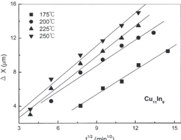
Average thicknesses (⌬X) of various intermetallic compounds were measured and plotted against the square root of reaction time (t):
where k represents the growth rate constant. Figures 7–9 show that the growth of Cu16In9, Cu11In9, and CuIn intermetallic compounds follows a parabolic re-lationship, implying that the growth of all inter-metallic layers is diffusion-controlled. In this case, the Arrhenius equation can be employed to express the growth rate constant for the intermetallic layers:
where A is a constant, Q the activation energy, R the
k A Q RT = − exp ∆X= k t( )1 2/
between Liquid Indium and Copper Substrates 491
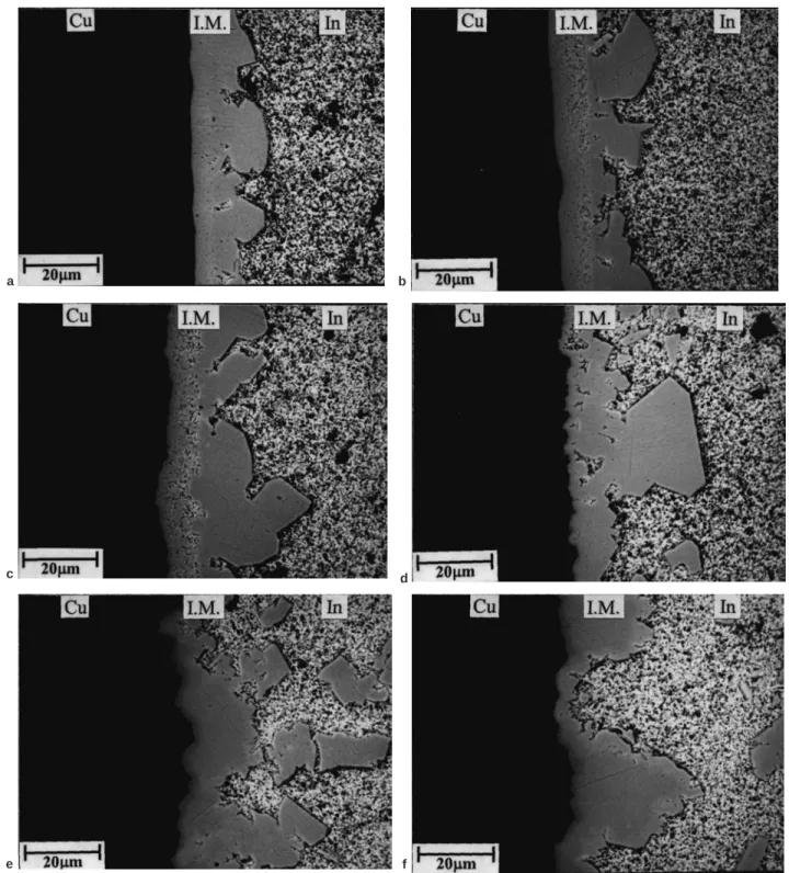
a b
c d
e f
Fig. 4. Microstructures of intermetallic compounds after Cu/In interfacial reactions at various temperatures for 120 min: (a) 175°C, (b) 200°C, (c) 250°C, (d) 300°C, (e) 350°C, and (f) 400°C.
gas constant, and T the absolute temperature. An Arrhenius plot of ln k vs. 1/T for the growth of vari-ous intermetallic compounds is given in Fig. 10. The activation energies (Q) for the growth of Cu16In9, Cu11In9, and CuIn as calculated from the plot are 59.5, 16.9, and 23.5 kJ/mole, respectively.
CONCLUSIONS
Soldering reactions between liquid In and Cu sub-strates at temperatures above 300°C result in the formation of a scallop-shaped Cu16In9 intermetallic
compound. Below 300°C, the scallop-shaped Cu11In9 and a continuous CuIn compound grow in opposite directions away from the original Cu/In interface. Se-lective etching of the In solder after reaction shows that the CuIn intermetallic compound contains spheroids rich in the In element at the boundaries.
Kinetics analyses show that the growth of Cu16In9, Cu11In9, and CuIn intermetallic compounds at the Cu/In interface is diffusion-controlled with ac-tivation energies being 59.5, 16.9, and 23.5 kJ/mole, respectively.
Fig. 5. Copper content of the intermetallic layer formed at 400°C for 120 min as a function of distance (d) from the Cu/IM interface.
Fig. 6. Copper content of the intermetallic double layer formed at 250°C for 120 min as a function of distance (d) from the Cu/IM inter-face.
Fig. 7. Average thickness of the Cu16In9 intermetallic compound
(⌬X) formed at temperatures above 300°C as a function of the square root of time (t1/2).
Fig. 8. Average thickness of the Cu11In9 intermetallic compound
(⌬X) formed at temperatures below 300°C as a function of the square root of time (t1/2).
Fig. 9. Average thickness of the CuIn intermetallic compound (⌬X) formed at temperatures below 300°C as a function of the square root of time (t1/2).
Fig. 10. Arrhenius plots of growth rate constants (k) for various inter-metallic compounds formed at the Cu/In interface.
between Liquid Indium and Copper Substrates 493
REFERENCES
1. K. Shimizu, T. Nakanishi, K. Karasawa, K. Hashimoto, and K. Niwa, J. Electron. Mater. 24, 39 (1995).
2. W.K. Jones, Y. Liu, M. Shah, and R. Clarke, Soldering Sur-face Mount Technol. 10, 37 (1998).
3. L.S. Goldmann, R.D. Herdzik, N.G. Koopman, and V.C. Mar-cotte, IEEE Trans. Parts, Hybrids and Packaging, PHP-13 3, 194 (1977).
4. P.T. Vianco A.C. Kilgo, and R. Grant, J. Mater. Sci. 30, 4871 (1995).
5. I. Manna, S. Bader, W. Gust, and B. Predel, Phys. Status So-lidi (a) 119, K9 (1990).
6. C.R. Kao, Mater. Sci. Eng. A: Struct. Mater.: Prop., Microstr. Processing A23, 196 (1997).
7. L.H. Su, Y.W. Yen C.C. Lin, and S.W. Chen, Metall. Mater. Trans. B 28B, 927 (1997).
8. R. Roy and S.K. Sen, J. Mater. Res. 7, 1377 (1992). 9. Y.C. Chen and C.C. Lee, Thin Solid Films 283, 243 (1996).