Electron spillover effects in In Ga N Ga N quantum-well lasers
Shyh-Jer Huang and Shun-Tung Yen
Citation: Journal of Applied Physics 102, 113112 (2007); doi: 10.1063/1.2821411 View online: http://dx.doi.org/10.1063/1.2821411
View Table of Contents: http://scitation.aip.org/content/aip/journal/jap/102/11?ver=pdfcov Published by the AIP Publishing
Articles you may be interested in
Excitonic properties of polar, semipolar, and nonpolar In Ga N Ga N strained quantum wells with potential fluctuations
J. Appl. Phys. 103, 093501 (2008); 10.1063/1.2903592
Carrier distribution in ( 0001 ) In Ga N Ga N multiple quantum well light-emitting diodes Appl. Phys. Lett. 92, 053502 (2008); 10.1063/1.2839305
Optical anisotropy in ultraviolet In Ga N Ga N quantum-well light-emitting diodes with a general crystal orientation
Appl. Phys. Lett. 92, 011130 (2008); 10.1063/1.2827581
Gain suppression phenomena observed in In x Ga 1 x N quantum well laser diodes emitting at 470 nm Appl. Phys. Lett. 89, 241127 (2006); 10.1063/1.2404971
Many-body optical gain of Ga In N As Ga As strained quantum-well lasers Appl. Phys. Lett. 85, 890 (2004); 10.1063/1.1779961
Electron spillover effects in InGaN / GaN quantum-well lasers
Shyh-Jer Huang and Shun-Tung Yena兲
Department of Electronics Engineering, National Chiao Tung University, Hsinchu, Taiwan 30050, Republic of China
共Received 29 May 2007; accepted 13 October 2007; published online 10 December 2007兲 The effects of electron spillover from quantum wells on the optical property of InGaN/GaN laser diodes are theoretically studied in detail. A six-band model including strain effects is used to calculate valence band states. Continuous subbands unconfined to the quantum wells are simulated deliberately by densely discretized subbands for the spillover electrons. The calculation results show obvious differences in the radiative current densities and the gain spectra between the cases with and without considering the spillover effect. We further investigate the spillover effect on the radiative current densities and the spontaneous emission spectra, with variations in the depth and the width of quantum wells, the total loss of the cavity, and the temperature. For shallow wells, the spillover effect is particularly important. It broadens both the gain and the spontaneous emission spectra and hence deteriorates the threshold of laser diodes. Such an effect can be alleviated by employing a long cavity and a multi-quantum-well active region. The concept of the electron spillover studied in this work is not only applicable to the nitride lasers but also to other kinds of quantum-well lasers. © 2007 American Institute of Physics.关DOI:10.1063/1.2821411兴
I. INTRODUCTION
In recent years there has been a lot of research effort in exploring blue-violet light sources, such as light-emitting di-odes 共LEDs兲 and laser diodes 共LDs兲, due to their potential applications in full-color displays and high-density optical storage. Potential materials for the short-wavelength emis-sion include SiC-,1 ZnSe-,2,3 and GaN-based wide-gap semiconductors.4Among them, the nitrides, such as GaN and the related ternary 共AlGaN and InGaN兲 and quaternary 共AlGaInN兲 compounds, are considered more promising for high-brightness emission, and currently they have been used commercially in making up blue-violet and green LEDs and LDs. However, the reliability of the wide-gap nitride LDs is still an important issue because of their short lifetime caused by high threshold current. In comparison with conventional zinc-blende GaAs-based lasers, the high threshold current of the wurtzite nitride lasers may be attributed to several fac-tors, including immature material preparation, the intrinsic large density of states in the valence bands, and large leakage current in the device structures not yet optimized.
The leakage current can be regarded as composed mainly of three components according to their different ori-gins: 共1兲 the component caused by nonradiative recombina-tion of electrons and holes in the active region, 共2兲 the one due to electron leakage from the active region to the p-type cladding layers,5 and 共3兲 the one caused by the interband transition of high-energy carriers in the neighborhood of the active region.5 The leakage current due to nonradiative re-combination has been considerably alleviated in the GaN lasers by the reduction of defects with the progress of mate-rial growth and device processing technologies.6,7As to the electron leakage into the p-type cladding layer, it has been commonly found from recent works that such leakage can be
reduced significantly by the insertion of an AlGaN electron blocking layer 共EBL兲 between the active region and the p-type layer.8–12 Furthermore, it has been demonstrated that this leakage can be made very low compared to other leak-ages by optimization on the structure with EBL.9–12The hole leakage out of the active region can be neglected because of the large effective mass of the inertial holes. The EBL, how-ever, cannot suppress the spillover of energetic carriers into the continuous subband states above the barriers in energy surrounding the quantum wells 共QWs兲 of the active region. Interband transition involving the high-energy spillover car-riers usually gives a negligibly small contribution to the op-tical peak gain of the QW active region but may cause sig-nificant consumption of electric current. Therefore, the recombination of spillover carriers can be regarded as one of the paths for the leakage current. Such a problem of carrier spillover depends on temperature and is particularly serious for electrons in the conduction bands because of the small electron effective mass, the large asymmetry between the densities of states of the conduction and valence bands, and the narrow QWs usually used in the nitride LDs. There are quite few literatures discussing leakage due to the recombi-nation of spillover carriers,5and so far, the influences of the optical transitions from the spillover carriers on the shapes of gain and spontaneous emission spectra have not been dis-cussed and analyzed in detail. Furthermore, there has not been any research work on this problem for the short-wavelength nitride LDs.
In this paper, we present the calculation results of the carrier spillover effects on the optical gain, the spontaneous emission, and the threshold current for InGaN/GaN QW LDs. The calculation is based on the six-band model for the valence band states. Continuous subbands above the barriers in energy are deliberately treated for the spillover carriers. We found that the electron spillover can broaden the gain and
a兲Electronic mail: [email protected].
共2007兲
0021-8979/2007/102共11兲/113112/8/$23.00 102, 113112-1 © 2007 American Institute of Physics
the spontaneous emission spectra, deteriorating the threshold of QW LDs. A multi-QW structure is then proposed to solve the problem.
This paper is organized as follows. The calculation ap-proaches are described in the following section. We then present our calculation results with detailed discussion in Sec. III. Finally, we draw the conclusion in Sec. IV.
II. CALCULATION APPROACHES
We consider the wurtzite III-nitride lasers with a conven-tional step separate-confinement heterostructure that contains an undoped active region of strained InGaN/GaN QWs and is inserted with an AlGaN EBL immediately near the QWs.10 The layers are considered to be grown on strain-free GaN along the crystallographic c-axis which is defined as the z-axis. We take the flatband approximation to calculate the band structure of the QWs. This is a good approximation for narrow QWs considered in this study, even if the strain-induced piezoelectric field in the InGaN QWs may be considerable.13At threshold condition, the piezoelectric field is strongly suppressed by the screening of the large density of carriers 共generally in the range of 1019– 1020 cm−3兲, fur-ther justifying the flatband approximation. It has also been pointed out that, in this range of threshold carrier density, there is a small difference from the case of full screening in the transition energy and the recombination rate between the lowest conduction and valence subbands.14 Franssen et al. have experimentally demonstrated that the polarization-induced electric field can be almost fully screened in nitride LDs close to lasing threshold, supporting our assumption of the flatband approximation.15
The valence band structure of the InGaN/GaN QWs is calculated based on the six-band k · p model which includes the coupling of the heavy-hole, the light-hole, and the spin-orbit split-off bands.16,17The strain effect is also included in this model. By means of a unitary transformation of basis functions, the 6⫻6 Hamiltonian in the six-band model can be block diagonalized into one consisting of two 3⫻3 blocks,17 Hˆ 共kˆz;kt兲 =
冋
Hˆ+共kˆz;kt兲 0 0 Hˆ−共kˆ z;kt兲册
, 共1兲 with Hˆ±=冤
Fˆ Kt ⫿iHˆt Kt Gˆ ⌬ ⫿ iHˆt ±iHˆt† ⌬ ± iHˆt† ˆ冥
, 共2兲 Fˆ = ⌬1+⌬2+ˆ +ˆ , Gˆ = ⌬1−⌬2+ˆ +ˆ , ˆ = ប2 2m0 共kˆzA1kˆz+ A2kt 2兲 + D 1⑀⬜+ 2D2⑀储, ˆ = ប2 2m0 共kˆzA3kˆz+ A4k2t兲 + D3⑀⬜+ 2D4⑀储, Kt= ប2 2m0 A5kt2, Hˆt= ប2 2m0 kt冑
2关kˆz共1 +冑
2A6− A1− A3兲 − 共1 − A1− A3兲kˆz兴, ⌬ =冑
2⌬3, and kˆz= − i/z, 共3兲where m0 is the free electron mass and kt=
冑
kx2 + ky
2 is the magnitude of the in-plane wave vector. The parameters⌬i共i
= 1 – 3兲 account for either the crystal-field split energy 共⌬1兲 or the spin-orbit interactions 共⌬2 and⌬3兲. The Ai共i=1–6兲 are
effective-mass-like parameters and the Di共i=1–4兲 are
defor-mation potential constants. The normal strain components⑀⬜ and⑀储in the QW region are given by
⑀储=
a0− a
a and⑀⬜= − 2C13
C33 ⑀储, 共4兲
where a0and a are the lattice constants of undeformed ma-terials making up the substrate and the QWs, which in the present study are GaN and InGaN, respectively. C13and C33 are stiffness constants of the QW material.
Based on the k · p model, the wave functions of valence band states can be expressed as
⌿±共r;k t兲 = 1
冑
Ae ikt·rt兺
=1 3 ±共kˆz;kt兲u±, 共5兲which, together with their energy E, can be solved by the effective-mass equation,
兺
=1 3 关Hˆ± 共kˆ z;kt兲 + Ev 0共z兲␦ 兴±= E±, = 1,2,3, 共6兲 where the±are envelope functions and the u±are the trans-formed basis functions according to which the Hamiltonians Hˆ± are built up;16,17A is the area of the QWs; rtand ktarethe in-plane position vector and the wave vector of the par-ticle, respectively; Ev0共z兲 is the z-dependent valence band edge of the undeformed materials composing the heterostruc-ture. It is noticed that the order of the operators in Eq.共3兲is of importance to the correct boundary conditions for match-ing the envelope functions.17
For the conduction band states, we use the single-band effective-mass equation,
冋
− z ប2 2mz z+ ប2k t 2 2mt + Ec 0共z兲 + a cz⑀⬜+ 2act⑀储册
= E, 共7兲 to solve the envelope functionand the energy E, where mz共mt兲 is the electron effective mass in the direction along
共transverse to兲 the growth direction; Ec
0共z兲 is the z-dependent conduction band edge of the undeformed materials compos-ing the heterostructure; acz and act are the deformation
po-tentials for the conduction bands along and transverse to the
113112-2 S.-J. Huang and S.-T. Yen J. Appl. Phys. 102, 113112共2007兲
c-axis, respectively. Neglecting the small spin-splitting ef-fect, we can write down the wave functions of conduction band states for spin up and spin down as simply a product of the envelope part and the Bloch function part,
⌽±共r;k t兲 = 1
冑
Ae ikt·rt共z;k t兲uc ± , 共8兲where uc± are the conduction band Bloch functions at the⌫ point for spin up共⫹兲 and spin down 共⫺兲.
Besides the discrete subbands bound by the barriers, we also consider the spillover of carriers to the continuous sub-band states which are above at least one side of the potential barriers in energy. We obtain the wave functions and the energy of the continuous subband states also using Eqs. 共5兲–共8兲, similar to the bound subband states, except that we use two infinite boundaries at positions sufficiently far away from each other for the continuous subbands, as illustrated in Fig. 1, where we include the EBL in the structure. Conse-quently, we obtain discrete subbands dense enough to realis-tically simulate the physical property of the real continuous subbands. Such infinite boundaries have been employed for the calculation of the continuous subband states in previous articles.5,18 Justification and detailed discussion for the infi-nite boundaries can be found there.
To calculate the gain spectrum of the active region as a function of the carrier concentration, we assume that the electrons and the holes are in quasiequilibrium in the con-duction bands and the valence bands, respectively, and that the electron sheet density is equal to the hole sheet density in the active region. It is therefore possible to determine the conduction band quasi-Fermi level Fcand the valence band
quasi-Fermi level Fv for a given sheet carrier density na in
the active region by the integrals
na= 2
兺
i冕
Pi c共k t兲fi c共F c,kt兲 kt 2dkt =兺
=±兺
j冕
Pj共kt兲关1 − fj共Fv,kt兲兴 kt 2dkt, 共9兲 where the factor 2 in Eq. 共9兲 accounts for the spin degen-eracy in the conduction band. The functions fic共Fc, kt兲 andfj共Fv, kt兲 are the Fermi-Dirac distribution functions for the
probabilities of electrons occupying the states ⌽i
±共r;k
t兲
=共1/
冑
A兲eikt·rti共z;kt兲uc± of conduction subband i and the
state ⌿j共r;kt兲=共1/
冑
A兲eikt·rt兺=13 j共kˆz; kt兲u of valencesubband j, respectively; Pi c共k
t兲 and Pj共kt兲 are the
probabili-ties of finding the carriers at states ⌽i
±共r;k
t兲 and ⌿j共r;kt兲,
respectively, in the active region with width Laand can thus
be expressed by Pi c共k t兲 =
冕
La 兩i共z;kt兲兩2dz, 共10兲 Pj共kt兲 =兺
=1 3冕
La 兩j共kˆz;kt兲兩2dz.For a given sheet carrier concentration, the optical gain g共ប兲 and the spontaneous emission rate rsp共ប兲 are then calculated using the formulas19
g共ប兲 = 关1 − e关ប−共Fc−Fv兲兴/kBT兴
兺
ij gsp,ije 共ប兲, e = x,y,z, 共11兲 rsp共ប兲 =兺
ij rsp,ij共ប兲, 共12兲 gsp,ije 共ប兲 = 2q 2 nrc⑀0m0 2 Lij=±兺
冕
兩Me,ij 兩2 fi c共1 − f j 兲␥/ 共Eij−ប兲2+␥2 ⫻ kt 2dkt, 共13兲 rsp,ij共ប兲 = nr 22 2បc2 2gsp,ijx + gsp,ijz 3 , 共14兲where is the angular frequency of the photon, T is the temperature, the superscript e is used to specify the polariza-tion of the optical electric field, nris the averaged refractive
index of the materials constituting the active region, q is the elementary charge, and⑀0 and c are the permittivity and the speed of light in vacuum, respectively; Eij⬅Ei
c共k
t兲−Ej共kt兲 is
the interband transition energy between the conduction sub-band state⌽i+共r;kt兲 关or ⌽i−共r;kt兲兴 with energy Ei
c共k
t兲 and the
valence subband state⌿j共r;kt兲 with energy Ej共kt兲. Lijis the
width of the region in which the interband process occurs between conduction subband i and valence subband j. Obvi-ously, if both the subbands i and j are continuous, Lij= L;
otherwise, Lij= La.␥−1is the intraband relaxation time which
we assume to be 0.1 ps. Me,ij is the e-component of the momentum-matrix element for interband transition between
FIG. 1. Schematic illustration of the band diagram of the neighborhood of the InGaN/GaN QW active region inside which four different kinds 共bb, cb, bc, and cc兲 of interband processes occur. The cb 共bb兲 process means the interband process between the continuous共bound兲 conduction and the bound valence subbands while the bc共cc兲 means the process between the bound 共continuous兲 conduction and the continuous valence subbands. The well has a width Lwand the active region has a width La. The continuous subbands
are simulated by dense discrete subbands that are discretized using two infinite potential boundaries. An AlGaN EBL is placed immediately near the active region.
the states ⌽i+共r;kt兲 关or ⌽−i共r;kt兲兴 and ⌿j共r;kt兲, with a
modulus squared given by19 兩Mx,ij 兩2=兩My,ij 兩2=
m0Epx
8 =1,2
兺
兩具i兩j典兩2, 共15兲
for the TE-polarization component, and 兩Mz,ij 兩2=
m0Epz
4 兩具i兩=3,j
典兩2, 共16兲
for the TM-polarization component, where the parameters Epxand Epzare defined as
Epx=
冉
m0 mt − 1冊
Eg 共Eg+⌬1+⌬2兲共Eg+ 2⌬2兲 − 2⌬3 2 共Eg+⌬1+⌬2兲共Eg+⌬2兲 − ⌬32 , 共17兲 Epz=冉
m0 mz − 1冊
共Eg+⌬1+⌬2兲共Eg+ 2⌬2兲 − 2⌬3 2 Eg+ 2⌬2 .The component rsp,ijof the spontaneous emission rate is due to the recombination of electrons in conduction subband i and holes in valence subband j. It has the meaning of the number of emitting photons due to the recombinations per unit time per unit volume per unit photon energy interval at energyប. Accordingly, the corresponding component of the resulting radiative recombination current density can be writ-ten as
Jij= qLij
冕
rsp,ij共ប兲dប. 共18兲 The total current density J =兺ijJij, which is the sum of allcurrent density components Jij, can also be considered as
composed of four components, J = Jbb+ Jbc+ Jcb+ Jcc. As
il-lustrated in Fig.1, the component Jbbis caused by the
tran-sitions from all the bound conduction subbands to all the bound valence subbands, the Jbcone is caused by the
transi-tions from all the bound conduction subbands to all the con-tinuous valence subbands, and Jcb共Jcc兲 is caused by the
tran-sitions from all the continuous conduction subbands to all the bound共continuous兲 valence subbands. These current compo-nents can be obtained by
Jbb=
兺
i b兺
j b Jij, Jbc=兺
i b兺
j c Jij 共19兲 Jcb=兺
i c兺
bj Jij, and Jcc=兺
i c兺
cj Jij,where the symbols b and c over the sigmas mean summa-tions over bound subbands and continuous subbands, respec-tively. For convenience in later analysis, the optical gain g and the spontaneous emission rsprate are also considered as composed of four components 共g=gbb+ gbc+ gcb+ gcc and
rsp= rsp,bb+ rsp,bc+ rsp,cb+ rsp,cc兲 with their expressions similar to Eq. 共19兲. It has been mentioned above that the electron leakage into the p-type cladding layer can be alleviated by the employment of EBL. Moreover, the main interest here is the investigation on the radiative current density involving the transitions from the continuous states, so the electron
leakage over the EBL is ignored through this work. As for the leakage due to the nonradiative current, it relies on the material quality and processing technologies, and hence we skip this issue.
We are mainly interested in the effects of carrier spill-over on threshold. For the threshold condition, we use the formula
⌫ max
ប g共ប兲 =␣, 共20兲
where␣is the cavity loss,⌫ is the optical confinement fac-tor, and maxបg共ប兲 is the peak gain. From condition共20兲, we first obtain the quasi-Fermi levels, Fc and Fv, at
thresh-old. With Fc and Fv, we obtain the carrier distribution in
energy space, based on which we further calculate the gain spectra, the spontaneous emission rates, and the recombina-tion current densities at threshold.
III. RESULTS AND DISCUSSION
In this section we present the calculated results and de-tailed analysis of the optical gains, the spontaneous emission, and the recombination current densities for In0.2Ga0.8N/GaN QW lasers inserted with a 20 nm Al0.2Ga0.8N EBL under the influence of the carrier spillover. All the values of the mate-rial parameters used in our calculation can be found from Ref. 20for wurtzite GaN, InN, and AlN. The values for the ternary compounds InGaN and AlGaN are obtained by linear interpolation between the binary compounds, except for the band gap energy for which a bowing parameter of 1.4 eV is used for InGaN and that of 0.7 eV for AlGaN.20 The band offset is a factor important in studying the spillover of carri-ers from the bound subbands. Unfortunately, till now there have been no compelling unambiguous values for the band offset of the nitride heterointerfaces. We thus take the va-lence band offset 共VBO兲 ⌬Ev or equivalently the valence
band partition ratio Qv as a variable parameter, where ⌬Ev
= Qv⌬Eg 共⌬Eg is the band gap difference兲, and investigate
the dependence of carrier spillover on the band offset. In the determination of the threshold condition, we assume that the lasers have structures such that the confinement factor ⌫=3 ⫻10−4L
a, where La is the active region width in units of
angstroms. This gives⌫=1.5% for a 50 Å QW, a value rea-sonable for typical III-nitride LDs. The total loss of the cav-ity is set at␣= 60 cm−1for the threshold condition关Eq.共20兲兴 except in the case where the loss␣ is considered as a vari-able parameter. The temperature is set at T = 300 K except in the case where we investigate the dependence of carrier sp-illover on temperature.
The density of carriers at threshold in our calculation is in the range from 2⫻1019to 6⫻1019 cm−3, depending on the well width, the cavity loss, and the temperature. At the high carrier concentration, it is feasible to employ the flat-band approximation in studying the effects of carrier spill-over for InGaN laser diodes here.
Figure2shows the current densities, J, Jbb, and J0, ver-sus the peak gain for single-QW structures with well widths Lw= 3.6 and 5.4 nm, assuming the partition ratios Qv= 0.33
in panel共a兲 and Qv= 0.45 in panel共b兲. Here, for comparison,
we include the current density J0which is calculated without
113112-4 S.-J. Huang and S.-T. Yen J. Appl. Phys. 102, 113112共2007兲
considering the continuous subbands; that is, in calculating J0 we assume all the carriers to be at the bound subband states. In our calculation, it is found that the current-density components Jbc and Jcc, involving the valence continuous
subbands in the transition processes, are negligibly small compared with the other components Jbb and Jcb. This is
because the density of states of the valence bands is much higher than that of the conduction bands. All the holes hence almost lie in the lowest bound subbands. Therefore we do not show the curves for Jbcand Jccin Fig.2 and henceforth
we will not present calculated results concerning transition processes involving the continuous valence subbands. As a result, the difference J − Jbb⯝Jcbcan reveal the influence of
electron spillover into the continuous subbands on the threshold current density. The electron spillover is more prominent as more carriers are injected into the active region. This leads to an increase in the difference J − Jbb with the
peak gain, as can be seen from the figure. It is also found that the difference J − Jbbis larger for larger Qvsince the spillover
of electrons is more prominent from a shallower QW. For Qv= 0.45, the difference J − Jbb is larger for Lw= 5.4 nm in
general than for Lw= 3.6 nm. Since the currents also depend
on the well width, one cannot conclude that the electron spillover is more considerable in a wider well. Contrarily, more percentage of electrons spill from the narrower well for which the bound subband edges are closer to the barrier. It should be noted that for Qv= 0.45 there is an appreciable
difference between J and J0both for Lw= 3.6 nm at threshold
共max g⯝5600 cm−1兲 and for L
w= 5.4 nm at threshold
共max g⯝3700 cm−1兲. This means that one may obtain an incorrect threshold current without the electron spillover ef-fect taken into account and also may have a misunderstand-ing of the carrier distribution both in energy and in space. As
will be seen later, such an incorrect carrier distribution may cause a significant deviation of gain and spontaneous emis-sion spectra.
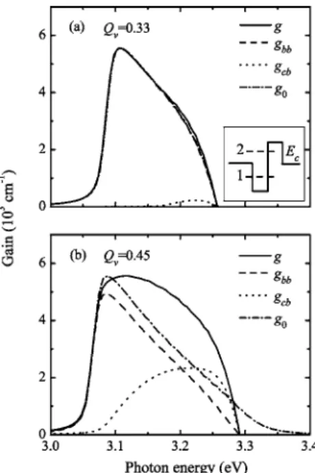
To give an insight into the carrier spillover effect on the optical property of QW active regions, we show in Fig.3the gain spectra g and their components gbband gcbat threshold
for single-QW structures with Lw= 3.6 nm, assuming Qv
= 0.33 in panel 共a兲 and Qv= 0.45 in panel 共b兲. For
compari-son, we also show the gain spectra g0 which are obtained without considering the carrier spillover. By comparing the curves in both the panels, we find that the electron spillover effect can be neglected for Qv= 0.33, but for Qv= 0.45 the
component gcbgives more contribution to the total gain g in
the high-energy range, resulting in a broader gain spectrum g, due to a larger number of electrons spilling over to the continuous subband states. The spillover also results in a significant blueshift of the peak gain. However, gcb gives
only a small contribution to the peak gain although, as has been seen in Fig. 2共b兲, the cb process can give a significant current density Jcb. There is a qualitative difference between
the profiles of the gain spectra g and g0 for Qv= 0.45. The
long tail of the g0spectrum for Qv= 0.45 is caused by a broad
distribution of electrons in the two-dimensional momentum space.
It should be mentioned that, among the continuous sub-bands, the lowest quasibound subband and those around it in energy provide the states for electrons that are dominant in the cb transition process. Inseted in Fig. 3共a兲is the conduc-tion band profile of the QW with the level of the lowest bound subband edge共level 1兲 and that of the lowest quasi-bound subband edge 共level 2兲. The quasibound subband states form a standing wave in the z direction and thus have
FIG. 2. The current densities, J, Jbb, and J0, vs the peak gain for In0.2Ga0.8N/GaN single-QW LDs with well widths Lw= 3.6 and 5.4 nm,
as-suming the partition ratio Qv= 0.33 in panel共a兲 and Qv= 0.45 in panel共b兲. J
is the total current density, Jbbis due to the bb process, and J0is calculated without considering the continuous subbands.
FIG. 3. The gain spectra at threshold for In0.2Ga0.8N/GaN single-QW struc-tures with Lw= 3.6 nm, assuming Qv= 0.33 in panel 共a兲 and Qv= 0.45 in
panel共b兲. The spectra g are the total gain, the spectra gbb共gcb兲 are due to the
bb共cb兲 process, and the g0ones are obtained without considering the con-tinuous subbands. Inseted is an illustration of the conduction band profile of the QW with the level of the lowest bound subband edge共level 1兲 and that of the lowest quasibound subband edge共level 2兲.
a nature of resonance. Because of the resonance nature, the wave functions of the quasibound subbands and their neigh-bors are much more localized around the QW than those of other subbands. As a result, these more localized subband states give a much larger interband matrix element Me,ij than others and hence play a dominant part in the cb process.
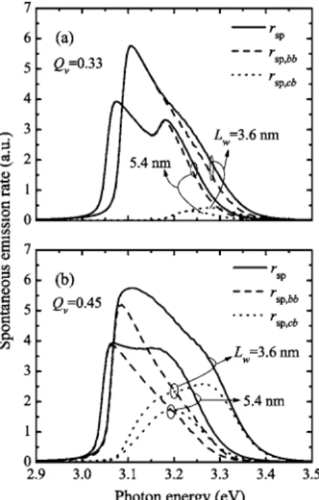
The cb process can also cause broadening of the sponta-neous emission spectrum. Figure 4 shows the spectra rsp of the total spontaneous emission rate and their components rsp,bb and rsp,cb at threshold for single-QW structures with Lw= 3.6 and 5.4 nm, similarly assuming Qv= 0.33 in panel
共a兲 and Qv= 0.45 in panel共b兲. As expected, the spectra rspare broader for Qv= 0.45 compared to those for Qv= 0.33
be-cause of more contribution from rsp,cbfor the shallower elec-tron QW. For the narrower QW共Lw= 3.6 nm兲 the numbers of
carriers needed for threshold are larger, giving the higher and broader spectra rsp. It can be found that there is a subordinate peak at photon energy of 3.18 eV in rsp,bb 共and rsp兲 for Qv
= 0.33 and Lw= 5.4 nm. No distinct subordinate peak is found
in the other rsp,bbspectra. Such a subordinate peak is caused mainly by the optical transition from the second bound con-duction subband which does not exist in the other QW struc-tures.
As is well known, for QW lasers the threshold current density J increases as the well width Lw decreases in the
range of small well width. This is because the number of carriers needed for threshold increases superlinearly with de-creasing Lw. On the other hand, in the range of large well
width, the threshold current also increases with increasing Lw
because of the wide active region for carrier recombination. As a result, one expects a minimum value of J in the J − Lw
curve at an optimum Lw. Nevertheless, the carrier spillover
makes the situation more complicated. To see this, we show in Fig.5the ratio Jcb/J at threshold versus the well width Lw
with Qv as a variable parameter. Such a Jcb/J ratio can be
considered as a measure of the electron spillover to the con-tinuous subbands. As expected, the spillover 共and thus the ratio Jcb/J兲 is more serious for larger Qv. For a small well
width, the spillover is more sensitive to the variation of Qv
when Qv is larger 共for a shallower electron QW兲. As Lw
increases from a small value 共2.4 nm兲, each of the ratios Jcb/J first decreases to a local minimum and then goes up.
The decrease of Jcb/J with increasing Lw is caused by the
increase of the optical confinement factor⌫ that reduces the carrier density needed for threshold and then alleviates the spillover of electrons to the continuous subbands. However, with increasing Lw, the lowest quasibound subband moves
downward and the separation decreases between the bound and the lowest quasibound subbands. This increases the elec-tron spillover to the lowest quasibound subband and its neighbors. The interplay of the two counteractive effects causes the curves of Jcb/J to go down and then up with
increasing Lw until the lowest quasibound subband has its
edge below the barriers in energy and becomes the highest bound subband. Around the critical point at which the sub-band changes from a quasibound to a bound nature, Jcb/J
reaches a local maximum, as shown in the curves for Qv = 0.33 and 0.37 in Fig.5. To the right of the dashed line in the figure, the second bound subband appears and the curves again go down and then up, governed by the variations of the confinement factor ⌫ and the position of the new lowest quasibound subband. Such going down and then up of Jcb/J
continues as the Lw increases. Finally, as Lw→⬁, Jcb/J→0
which is the value for a three-dimensional active region. It can be found from Fig. 5 that the cb process may become dominant in the optical properties of the QW struc-tures if Lw becomes small for a large Qv. This situation
should be avoided to take advantage of low threshold in a two-dimensional QW.
Figure6 shows the current densities J and Jbbat
thresh-old as a function of Lwfor Qv= 0.33 and 0.45. Now we can
figure out the variations of the curves with the aid of the explications for Fig. 5. We can take a QW of width in the range of 3 – 5 nm for Qv= 0.33 and in the range of 4 – 6 nm
for Qv= 0.45 for a low threshold. From the viewpoint of
de-FIG. 4. The spectra of spontaneous emission rates at threshold for In0.2Ga0.8N/GaN single-QW structures with Lw= 3.6 and 5.4 nm, assuming
Qv= 0.33 in panel共a兲 and Qv= 0.45 in panel共b兲. The spectra rspare the total spontaneous emission rate and the rsp,bb共rsp,cb兲 ones are due to the bb 共cb兲 process.
FIG. 5. The ratio Jcb/J for In0.2Ga0.8/GaN single-QW LDs at threshold vs the well width Lwwith Qvas a variable parameter共Qv= 0.33, 0.37, 0.41, and
0.45兲. The dashed line indicates the boundary across which the lowest qua-sibound subband changes to a bound subband.
113112-6 S.-J. Huang and S.-T. Yen J. Appl. Phys. 102, 113112共2007兲
vice design, such wide ranges of well width can allow a freedom of choosing a desired emission wavelength from a wide spectral range. As expected, we find a minimum of Jbb
and a local maximum of Jcb= J − Jbb for Qv= 0.33 at Lw
= 4.8 nm around which the lowest quasibound subband changes to the highest bound subband.
The carrier spillover depends also on the cavity loss␣ that determines the carrier density required for threshold. Figure 7 shows the ratio Jcb/J at threshold versus the well
width Lwfor Qv= 0.33 and 0.45 with␣as a variable
param-eter. As the figure shows, the spillover can be significantly reduced by decreasing the cavity loss␣. This implies that a long cavity is preferred to alleviate the spillover effect, espe-cially when Qvis large.
As has been pointed out, the carrier spillover and the threshold current can be significantly reduced by increasing the well width Lw for a large Qv. However, this will cause
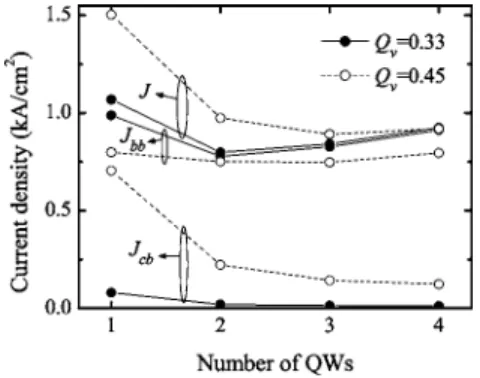
redshift in the emission wavelength and may sacrifice the purpose of short-wavelength emission. To reduce the elec-tron spillover and simultaneously keep a short-wavelength emission, one can employ a structure of multiple QWs. Fig-ure8shows the current densities J, Jbb, and Jcbat threshold
versus the number of QWs in the active region for Qv = 0.33 and 0.45. The width of each QW is fixed at Lw
= 3.6 nm. As can be seen, the current density Jcb is
consid-erably reduced for Qv= 0.45 as the QW number increases from 1 to 2. Consequently, this causes a considerable reduc-tion of the total threshold current density J for Qv= 0.45. As
the QW number changes from 2 to 3, there is a slight reduc-tion in Jcb but no appreciable change in Jbb for Qv= 0.45.
Further increasing the QW number does not significantly re-duce Jcb but causes an increase of Jbb, implying that a
triple-QW structure is preferred for a low threshold when Qv= 0.45. For Qv= 0.33, a double-QW structure seems pre-ferred for low threshold.
Finally, it is worthwhile to make clear the influence of temperature variation on the electron spillover since the heat dissipation is still a critical issue for the nitride LDs. The rise in temperature causes a broadening of carrier distribution in energy. Therefore, we also expect spectral broadening in the gain g and the spontaneous emission rate rsp with the tem-perature rising. This can be seen from Fig. 9, which is the plot of the g and the rspspectra of 3.6 nm single-QW struc-tures at two different temperastruc-tures T = 300 and 400 K for共a兲 Qv= 0.33 and共b兲 Qv= 0.45. The broadness of the spectra for
Qv= 4.5 at T = 400 K in Fig. 9共b兲 means that the electron
spillover is more serious at higher temperature when the QW is shallow.
Figure10shows the various current densities at thresh-old as functions of temperature T for the 3.6 nm single-QW
FIG. 6. The current densities J and Jbbfor In0.2Ga0.8/GaN single-QW LDs at threshold as a function of Lwfor Qv= 0.33 and 0.45.
FIG. 7. The ratio Jcb/J for In0.2Ga0.8/GaN single-QW LDs at threshold vs the well width Lwfor Qv= 0.33 and 0.45 with the cavity loss␣as a variable
parameter共␣= 40, 60, and 80 cm−1兲.
FIG. 8. The current densities J, Jbb, and Jcbof In0.2Ga0.8N/GaN multi-QW LDs at threshold vs the number of QWs for Qv= 0.33 and 0.45.
FIG. 9. The spectra of the gain g and the spontaneous emission rate rspat two different temperatures T = 300 and 400 K for 3.6 nm In0.2Ga0.8N/GaN single-QW LDs at threshold with共a兲 Qv= 0.33 and共b兲 Qv= 0.45.
structures with Qv= 0.33 and 0.45. With rising T, the Jcbat
threshold increases more for Qv= 0.45 than for Qv= 0.33 due to a smaller separation between the lowest quasibound and the true bound subbands for the shallower QW. Quite differ-ently, the Jbb decreases for Qv= 0.45 but increases for Qv
= 0.33 with rising T. This can be understood by the fact that the distribution probability function becomes flatter for a higher T and that the density of states around the quasibound subband edge is much larger than that of the bound subband. As a result, the electron density in the bound subband at threshold decreases for the shallow QW as T rises. However, the increase of the Jbbwith rising T for the deep QW is due
to the gain spectrum broadening that requires a high carrier density at threshold. It is noticed that for Qv= 0.45 the Jcb
becomes dominant over the Jbbas T⬎320 K, implying that
the optical property of the shallow QWs is no longer of pure two-dimensional nature. For deep QWs, the spillover is not serious in the range of T = 300– 400 K.
In this study, we have taken the valence band partition ratio Qv as a variable parameter because of lack of a
com-pelling value for this parameter. However, in the true case, Qvmust be fixed. It may be 0.33, or 0.45, or more probably
another value. Recent published works have come to an agreement that the value of Qv is small 共close to 0.3兲.21,22 Even for the small value, the spillover effect is not negligible on the threshold current. Nevertheless, regardless of the value of Qv, our present work has introduced the important concept of carrier spillover, applicable not only to the nitride LDs but also to other kinds of LDs such as short-wavelength AlGaInP/GaAs LDs.
We have presented the calculated results by assuming quasiequilibrium for electrons in the conduction band and for holes in the valence band. This means that our calculations are applicable to the case at and below threshold. Above threshold, the high interband transition rate makes the as-sumption of quasiequilibrium no longer the case. It causes the spectral hole burning of the distribution function, which may have a reduction of the electron population in the bound subbands and meanwhile an increase of the population in the continuous subbands. Consequently, we expect a sublinear L-I relation above threshold.
IV. CONCLUSION
The influences of spillover effects on radiative current density, gain spectra, and spontaneous emission spectra in InGaN/GaN QW LDs have been theoretically studied in de-tail. To this end, the continuous subbands above the barriers in energy are considered for the spillover electrons. It has been shown that there are obvious differences in the radiative current densities and gain spectra between the cases with and without considering the spillover effect. It is shown that the spillover effects are important, especially to shallow QWs. The participation of spillover electrons in interband transi-tions causes spectral broadening of the gain and the sponta-neous emission and hence increases the threshold current. Such effects become more serious as the cavity loss in-creases or the temperature rises. To reduce the spillover, one can employ a multi-QW structure for the LDs. The concept of electron spillover is important not only to the nitride LDs but also to other kinds of LDs that have a shallow QW and large asymmetry in density of states between the conduction and the valence bands.
ACKNOWLEDGMENTS
This work was supported by the National Science Coun-cil under Grant No. 95-2221-E-009-281 and MOE ATU Pro-gram of Republic of China.
1T. Yamaguchi, Y. Ueda, Y. Matsushita, K. Koga, and T. Niina, Optoelec-tron., Devices Technol. 7, 57共1992兲.
2W. Xie, D. C. Grillo, R. L. Gunshor, M. Kobayashi, H. Jeon, J. Ding, A. V. Nurmikko, G. C. Hua, and N. Otsuka, Appl. Phys. Lett. 60, 1999 共1992兲.
3D. E. Eason, Z. Yu, W. C. Hughes, W. H. Roland, C. Boney, J. W. Cook, Jr., J. F. Schetzina, G. Cantwell, and W. C. Harasch, Appl. Phys. Lett. 66, 115共1995兲.
4J. I. Pankove, E. A. Miller, and J. E. Berkeyheiser, RCA Rev. 32, 383 共1971兲.
5S. T. Yen and C. P. Lee, IEEE J. Quantum Electron. 33, 443共1997兲. 6S. Strite and H. Morkoç, J. Vac. Sci. Technol. B 10, 1237共1992兲. 7H. Morkoç, S. Strite, G. B. Gao, M. E. Lin, B. Sverdlov, and M. Burns, J.
Appl. Phys. 76, 1363共1994兲.
8S. Nakamura, M. Senoh, S. Nagahama, N. Iwasa, T. Yamada, T. Mat-sushita, Y. Sugimoto, and H. Kiyoku, Appl. Phys. Lett. 69, 1568共1996兲. 9J. Y. Chang and Y. K. Kuo, J. Appl. Phys. 93, 4992共2003兲.
10M. Hansen, J. Piprek, P. M. Pattison, J. S. Speck, S. Nakamura, and S. P. Denbaars, Appl. Phys. Lett. 81, 4275共2002兲.
11S. N. Lee, S. Y. Cho, H. Y. Ryu, J. K. Son, H. S. Paek, T. Sakong, T. Jang, K. K. Choi, K. H. Ha, M. H. Yang, O. H. Nam, Y. Park, and E. Yoon, Appl. Phys. Lett. 88, 111101-1共2006兲.
12S. P. Łepkowski and S. Krukowski, J. Appl. Phys. 100, 016103-1共2006兲. 13G. Martin, A. Botchkarev, A. Rockett, and H. Morkoç, Appl. Phys. Lett.
68, 2541共1996兲.
14F. D. Sala, A. D. Carlo, P. Lugli, F. Bernardini, V. Fiorentini, R. Scholz, and J. M. Jancu, Appl. Phys. Lett. 74, 2002共1999兲.
15G. Franssen, T. Suski, and P. Perlin, Appl. Phys. Lett. 87, 041109共2005兲. 16S. L. Chuang and C. S. Chang, Phys. Rev. B 54, 2491共1996兲.
17F. Mireles and S. E. Ulloa, Phys. Rev. B 60, 13659共1999兲. 18S. T. Yen, Phys. Rev. B 66, 075340共2002兲.
19S. L. Chung, IEEE J. Quantum Electron. 32, 1791共1996兲. 20I. Vurgaftman and J. R. Meyer, J. Appl. Phys. 94, 3675共2003兲. 21S. H. Wei and A. Zunger, Appl. Phys. Lett. 69, 2719共1996兲.
22C. Manz, M. Kunzer, H. Obloh, A. Ramakrishnan, and U. Kaufmann, Appl. Phys. Lett. 74, 3993共1999兲.
FIG. 10. The current densities J, Jbb, and Jcbat threshold as functions of
temperature T for the 3.6 nm In0.2Ga0.8/GaN single-QW LDs with Qv = 0.33 and 0.45.
113112-8 S.-J. Huang and S.-T. Yen J. Appl. Phys. 102, 113112共2007兲