This content has been downloaded from IOPscience. Please scroll down to see the full text.
Download details:
IP Address: 140.113.38.11
This content was downloaded on 28/04/2014 at 00:05
Please note that terms and conditions apply.
Formation of semiconductor quantum rings using GaAs/AlAs partially capped layers
View the table of contents for this issue, or go to the journal homepage for more 2004 Nanotechnology 15 848
(http://iopscience.iop.org/0957-4484/15/7/024)
INSTITUTE OFPHYSICSPUBLISHING NANOTECHNOLOGY
Nanotechnology 15 (2004) 848–850 PII: S0957-4484(04)76501-0
Formation of semiconductor quantum
rings using GaAs/AlAs partially capped
layers
Bing Chi Lee and Chien Ping Lee
Department of Electronic Engineering, National Chiao Tung University, Hsinchu, Taiwan, Republic of China E-mail: [email protected] Received 12 February 2004 Published 26 April 2004 Online at stacks.iop.org/Nano/15/848 DOI: 10.1088/0957-4484/15/7/024 Abstract
A new method for fabricating semiconductor quantum rings has been developed. Instead of using the conventional GaAs cap layer, we used the GaAs/AlAs cap layer for the ring formation. The additional AlAs layer impedes the inward diffusion of the Ga and Al atoms and results in nicely formed ring structures with a more relaxed growth condition. Because of this layer, the ring-shaped structure can be maintained with a higher annealing temperature without being washed out by the intermixing of Ga/Al with In in the central region of the dots. The shape and the strain distribution of quantum rings have also been characterized by transmission electron microscopy.
1. Introduction
Microscale and nanoscale metallic and semiconductor quantum rings have been studied experimentally for over a decade [1]. Advanced growth techniques such as molecular beam epitaxy (MBE) and metal–organic vapour phase epitaxy (MOVPE) have allowed us to produce semiconductor quantum rings in a single growth run [2–5]. Recent experimental results on InGaAs semiconductor quantum rings have demonstrated unusual excitation properties [6–11] such as the capability of trapping a single magnetic flux and possessing a large negative excitonic permanent moment. Such results provide undoubted evidence that the nanoscale surface ring-shaped morphology is able to exhibit quantum mechanical properties with rotational symmetry.
In addition to studies on the electronic and the optical properties of quantum rings, the fabrication techniques and the formation mechanism have also attracted much attention. InGaAs quantum rings were first fabricated as a result of the study of GaAs overgrowth on InAs quantum dots (QDs) [12]. By capping the InAs or InGaAs QDs with a GaAs layer thinner than the dot height and then following this with a short time annealing under an As flux, one is able to produce the ring-shaped structure by selectively removing the centre
part of the dots. However, experimental results show that the formation of the quantum rings is strongly dependent on the growth condition. The substrate temperature for the capping process and the molecular species of the As beam (As2 or As4) can greatly influence the growth of the rings. Two mechanisms [2–4, 13] have been proposed to explain the origin of the depression in the centre of rings: the diffusion-driven transformation and the dewetting process. The former comes from the kinetic effect. During annealing, mobile In atoms diffuse away from the central region of the dots and alloy with the less mobile Ga atoms at the rim of the dots, leaving a crater-like nanohole in the centre. This process, however, depends strongly on the annealing temperature used. If the temperature is too high, the Ga atoms may diffuse in and result in the dots being totally converted into InGaAs alloy dots. The second mechanism is based on dynamic considerations. The dewetting process originates from an outward pointing force resulting from the change in the surface free energy balance due to the thin cap layer overgrown on the dots. It is believed that both of these mechanisms contribute to the formation of the quantum rings.
Conventionally, the MBE growth of InAs quantum rings uses a GaAs cap layer with a carefully selected growth temperature and annealing temperature. In this work, we use
Formation of semiconductor quantum rings using GaAs/AlAs partially capped layers
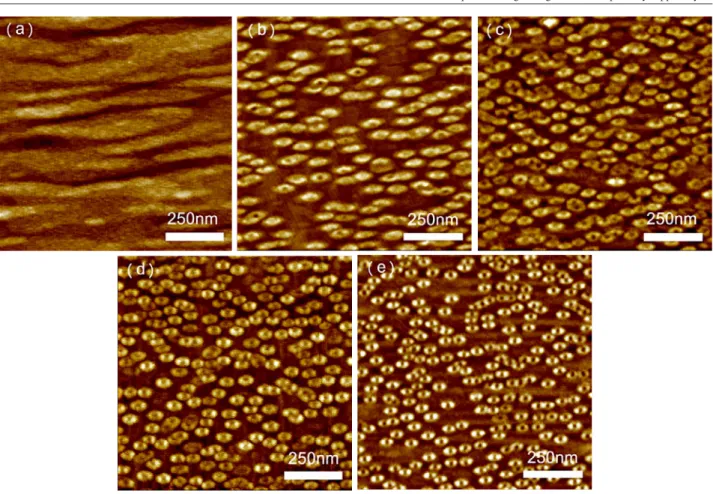
Figure 1. AFM images showing the surface morphology of quantum rings formed with different GaAs/AlAs cap layers. The thickness of
GaAs/AlAs is (a) 0/25 Å, (b) 5/20 Å, (c) 10/15 Å, (d) 15/10 Å and (e) 0/25 Å. (This figure is in colour only in the electronic version)
the composite AlAs/GaAs as the cap layer for the formation of quantum rings. Keeping the total cap thickness the same but varying the thickness of AlAs, different morphological changes in the quantum rings are obtained. By adding an additional AlAs layer on top of GaAs, we are able to reduce the surface mobility of group III atoms on the AlAs surface (because of the higher bonding strength of AlAs) and enhance the quantum ring formation. By investigating the surface morphology evolution with ex situ atomic force microscope (AFM), we found that AlAs plays an important role in the formation of quantum rings. In this way, the formation of quantum rings is not limited to a certain growth temperature for the cap layer. Also, this thin layer can preserve the ring shape even with an annealing temperature higher than the growth temperature.
2. Experimental procedure
Our experiment was carried out with a Varian Gen II solid source MBE system using As4 as the arsenic source. The sequence for the growth of quantum rings followed the standard procedure except for replacing the GaAs partially capped layer with a pair of GaAs/AlAs layers. The cap layer had a combined thickness of 25 Å and was grown at 520◦C. Although the total thickness was fixed, the thickness of each constituent layer was varied in order to see its effect on the quantum ring formation.
After the cap layer was deposited, the sample was annealed for 1 min under an As4flux.
Samples were grown on epi-ready GaAs(001) substrates. After the oxide layer was removed, a 2500 Å GaAs buffer was deposited at 570◦C. The substrate temperature was then lowered to 520◦C for the deposition of 2.6 monolayers (MLs) of InAs to form the QDs. A pair of GaAs/AlAs layers was deposited at the same temperature and then we raised the substrate temperature with a ramping rate of 20◦C to anneal the sample for 1 min. In the past, the same temperature was used for the annealing and the growth of the cap layer. A higher annealing temperature can wash out the ring structure because of the inward diffusion of the Ga atoms alloying with the In atoms in the central region of the dots. But here, because of the use of the AlAs in the cap layer, we were able to raise the annealing temperature without losing the ring structure. After the ring formation, the surface morphology of the samples was examined by a Digital Instrument Multimode AFM using the tapping mode.
3. Experimental results and discussion
The AFM images in figure 1 show the variations of the surface morphology for various combinations of the GaAs/AlAs cap layers. The thicknesses for the GaAs/AlAs layer were 25/0, 20/5, 15/10, 10/15 and 0/25 Å. The corresponding surface morphological images after annealing are shown in 849
B C Lee and C P Lee
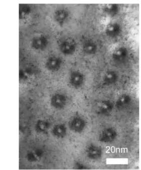
Figure 2. The plan-view TEM image shows the shape and strain
distribution of quantum rings.
figures 1(a)–(e), respectively. For a moderate overgrowth temperature, the adatoms diffuse preferentially along the [1¯10] direction resulting in an anisotropic shape. When the cap layer consists of GaAs only, the diffusion of the adatoms and the intermixing between In and Ga during annealing seem to be the fastest and that smooths out the surface morphology of the dots (see figure 1(a)). Under this condition, no rings are formed. When 5 Å of GaAs is replaced by AlAs in the cap layer, ring structures start to appear but not all dots turn into rings (see figure 1(b)). The elongated structure also becomes shorter. Because of the stronger bonding between Al and As, the surface diffusion of Al is much slower than that of Ga or In. So the preferential diffusion as seen in figure 1(a) is greatly reduced resulting in a shorter oval-shaped surface structure. The centre part of the InAs dots that is not covered by the cap layer moves to the rim to form rings. But because AlAs is not distributed uniformly over the surface during the first 3–4 MLs of growth and only a fraction of dots are covered with AlAs in the periphery, some of the structures do not form rings. Owing to the slowdown of Ga migration on the AlAs surface as well as a shorter diffusion length of Al, In–Ga alloy forms right at the periphery of the dots and the dewetting process caused by the imbalance of surface and interface forces leads to a crater-like structure. In contrast, when the partially capped layer contains no or a small amount of AlAs, the strong alloying in the dots due to the inward diffusion of the Ga atoms dominates over the dewetting process causing the formation of dash-like structures. Adding a thin AlAs layer slows down the inward diffusion of Ga atoms, and therefore prevents the ring-shaped morphology being washed out during annealing. When we further increase the thickness of AlAs, very nice quantum rings are formed. Figures 1(c) and (d), corresponding to samples with cap layers of 15 Å GaAs/10 Å AlAs and 10 Å GaAs/15 Å AlAs, are AFM microphotographs of the quantum rings. They have similar shapes but with figure 1(d)
showing a more symmetrical structure. Finally, the AFM image shown in figure 1(e) shows the quantum rings when the cap layer is totally AlAs.
In order to see the structure of the quantum rings more clearly, we characterized the sample capped with 25 Å AlAs using a transmission electron microscope (TEM). The plan-view TEM image in figure 2 shows the shape and strain distribution of the quantum rings. With the appearance of quantum rings, the strain distribution rearranges drastically. The bright spot with a diameter of ∼5 nm in the centre of the rings represents the crater-like nanohole originated from the dewetting process. The dark area at the border with base dimensions of ∼15 nm × 15 nm, the more highly strained region, exhibits composition variation at the edge of the crater and the rim due to the intermixing of the In atoms and the Al atoms.
4. Summary
In summary, we have demonstrated a very good method for achieving semiconductor quantum rings by using a GaAs/AlAs cap layer to cover the QDs prior to annealing. With the additional AlAs in the cap layer, the quantum rings that are formed are not limited to a certain growth condition and the ring topology is preserved even with a higher annealing temperature. In addition, we have also studied the structure of the rings and the strain/composition distribution in the rings using a TEM.
Acknowledgments
This work was supported by the National Science Council under contract No NSC 92-2120-E-009-002. The authors wish to thank Dr Xing-Jian Guo for his contribution to obtaining TEM images and for fruitful discussions.
References
[1] Aronov A G and Sharvin Yu V 1987 Rev. Mod. Phys. 59 755 [2] Lorke A, Blossey R, Garc´ıa J M, Bichler M and
Abstreiter G 2002 Mater. Sci. Eng. B 88 225
[3] Raz T, Ritter D and Bahir G 2003 Appl. Phys. Lett. 82 1706 [4] Granados D and Garc´ıa J M 2003 Appl. Phys. Lett. 82 2401 [5] Cui J, He Q, Jiang X M, Fan Y L, Yang X J, Xue F and
Jiang Z M 2003 Appl. Phys. Lett. 83 2907
[6] Lorke A and Luyken R J 1998 Physica B 256–258 424 [7] Pettersson H, Warburton R J, Lorke A, Karrai K, Kotthaus J P,
Garc´ıa J M and Petroff P M 2000 Physica E 6 510 [8] Lorke A, Luyken R J, Govorov A O and Kotthaus J P 2000
Phys. Rev. Lett. 84 2223
[9] Emperador A, Pi M, Barranco M and Lorke A 2000 Phys. Rev. B 62 4573
[10] Warburton R J, Sch¨aflein C, Haft D, Bickel F, Lorke A, Karrai K, Garc´ıa J M, Schoenfeld W and Petroff P M 2001
Physica E 9 124
[11] Warburton R J, Schulhauser C, Haft D, Sch¨aflein C, Karrai K, Garc´ıa J M, Schoenfeld W and Petroff P M 2002 Phys. Rev. B 65 113303
[12] Garc´ıa J M, Medeiros-Ribeiro G, Schmidt K, Ngo T, Feng J L, Lorke A, Kotthaus J and Petroff P M 1997 Appl. Phys. Lett.
71 2014
[13] Blossey R and Lorke A 2002 Phys. Rev. E 65 021603