Electrical characteristics and suppressed boron penetration behavior of thermally
stable HfTaO gate dielectrics with polycrystalline-silicon gate
Xiongfei Yu, Chunxiang Zhu, M. F. Li, Albert Chin, A. Y. Du, W. D. Wang, and Dim-Lee Kwong
Citation: Applied Physics Letters 85, 2893 (2004); doi: 10.1063/1.1795369
View online: http://dx.doi.org/10.1063/1.1795369
View Table of Contents: http://scitation.aip.org/content/aip/journal/apl/85/14?ver=pdfcov Published by the AIP Publishing
Articles you may be interested in
Study on characteristics of thermally stable HfLaON gate dielectric with TaN metal gate Appl. Phys. Lett. 93, 252903 (2008); 10.1063/1.3050522
Impact of titanium addition on film characteristics of Hf O 2 gate dielectrics deposited by atomic layer deposition J. Appl. Phys. 98, 054104 (2005); 10.1063/1.2030407
Physical and electrical properties of metal gate electrodes on HfO 2 gate dielectrics J. Vac. Sci. Technol. B 21, 11 (2003); 10.1116/1.1529650
Compatibility of polycrystalline silicon gate deposition with HfO 2 and Al 2 O 3 / HfO 2 gate dielectrics Appl. Phys. Lett. 81, 1288 (2002); 10.1063/1.1499514
Thermal stability and electrical characteristics of ultrathin hafnium oxide gate dielectric reoxidized with rapid thermal annealing
Appl. Phys. Lett. 76, 1926 (2000); 10.1063/1.126214
This article is copyrighted as indicated in the article. Reuse of AIP content is subject to the terms at: http://scitation.aip.org/termsconditions. Downloaded to IP: 140.113.38.11 On: Thu, 01 May 2014 04:10:45
Electrical characteristics and suppressed boron penetration behavior
of thermally stable HfTaO gate dielectrics with polycrystalline-silicon gate
Xiongfei Yu, Chunxiang Zhu,a) and M. F. Li
Silicon Nano Device Lab, Department of Electrical and Computer Engineering, National University of Singapore, Singapore 119260
Albert Chin
Department of Electronics, National Chiao Tung University, Hsinchu, Taiwan, ROC
A. Y. Du
Institute of Microelectronics, Singapore 117685
W. D. Wang
Institute of Material Research and Engineering, Singapore 117602
Dim-Lee Kwong
Department of Electrical and Computer Engineering, University of Texas, Austin, Texas 78752
(Received 25 February 2004; accepted 29 July 2004)
The thermal stability and electrical characteristics of HfTaO gate dielectric with polycrystalline-silicon gate have been investigated. The incorporation of Ta into HfO2enhances the crystallization temperature of film dramatically. Transmission electron microscopy micrographs confirm that HfTaO with 43% Ta film remains amorphous even after activation annealing at 950 ° C for 30 s, and the formation of low- interfacial layer is observably reduced. The capacitance– voltage curve of metal–oxide–semiconductor capacitor using HfTaO gate dielectric fits well with simulated curve, indicating good interface property between HfTaO and substrate. In addition, the boron penetration behaviors of HfTaO films are sufficiently suppressed as manifested by the narrow flat-band voltage shift. The negligible flat-band voltage shift in HfTaO with 43% Ta film is observed and attributed to its amorphous structure after device fabrication. © 2004 American Institute of
Physics. [DOI: 10.1063/1.1795369]
As complementary metal–oxide–semiconductor (MOS) devices continuously scale down to reach the 0.1m era, high-gate dielectrics are being investigated to replace con-ventional SiO2 and SiON gate dielectrics.
1
Among many candidates of the high- materials, HfO2 has been high-lighted due to its high dielectric constant共⬃25兲, relatively wide band gap共⬃5.8 eV兲, and calculated thermal stability in contact with Si.2However, HfO2crystallizes at temperatures below 500 ° C. Grain boundaries in crystallized gate dielec-tric can be the fast paths for oxygen and dopant diffusion into the gate dielectric and even to the channel region in the silicon substrate, causing low- interfacial layer growth, electrical instability, and defect generation.3To increase the crystallization temperature, silicon, aluminum, and nitrogen have been incorporated into HfO2 films to form HfSiO,4,5 HfAlO,6,7and their nitride.8,9All of these materials exhibit a high crystallization temperature and good thermal stability in contact with Si to withstand the conventional activation an-nealing at 900– 1000 ° C. Unfortunately, the dielectric con-stants of these materials are significantly degraded due to the incorporated low dielectric constant SiO2 or Al2O3 (⬃3.9 for SiO2 and⬃9 for Al2O3).
10
The degradation of dielec-tric constant compromises the benefit of high- gate dielectrics.
In this letter, both n-type and p-type MOS capacitors using ultrathin HfTaO gate dielectric with equivalent oxide thickness (EOT) of 15 Å have been investigated. Results
show that the incorporation of 43% Ta significantly increases the crystallization temperature of HfO2 up to 1000 ° C. The degradation of dielectric constant is also avoided due to the high dielectric constant of Ta2O5 共⬃26兲.
10
Since the HfTaO with 43% Ta film remains amorphous after activation annealing at 950 ° C for 30 s, remarkable suppression of low- interfacial layer growth and boron penetration were achieved.
The n+ polycrystalline-silicon/high-/ p-Si and p+ polycrystalline-silicon (poly-Si)/high-/ n-Si MOS capaci-tors were fabricated on 6 in. Si(100) wafers with a resistiv-ity of 10 ohm cm. After active area definition, standard pre-gate clean with diluted hydrofluoric-last processes were performed. In order to inhibit the formation of a low- inter-facial layer during deposition and high-temperature anneal-ing, surface nitridation treatment in NH3ambient was done at 700 ° C for 10 s. HfO2 and HfTaO with two different Ta composition films were deposited using reactive co-sputtering technique at room temperature, and the composi-tion of Ta was controlled by the ratio of applied power be-tween Hf and Ta targets. Post-deposition annealing(PDA) in N2ambient was followed by rapid thermal annealing(RTA) at 700 ° C for 40 s to form high-quality high- layer. Low-pressure chemical vapor deposition poly-Si with a thickness of 200 nm was deposited as a gate electrode. After gate pat-terning, phosphorous for n-type MOS devices was implanted at 50 keV with a dose of 5⫻1015cm−2. Boron-implanted
(boron, 20 keV, 5⫻1015cm−2) p-type MOS devices were used to investigate boron penetration behavior. Then dopant activation annealing was performed by RTA in N2 ambient a)Author to whom correspondence should be addressed; electronic mail:
APPLIED PHYSICS LETTERS VOLUME 85, NUMBER 14 4 OCTOBER 2004
0003-6951/2004/85(14)/2893/3/$22.00 2893 © 2004 American Institute of Physics
This article is copyrighted as indicated in the article. Reuse of AIP content is subject to the terms at: http://scitation.aip.org/termsconditions. Downloaded to IP: 140.113.38.11 On: Thu, 01 May 2014 04:10:45
(850–1000 °C, 30 s). Sintering was done at 420 °C in
form-ing gas ambient for 30 min after back side Al deposition. The compositions of HfTaO with 29% and 43% Ta(refer to Hf0.71Ta0.29Ox and Hf0.57Ta0.43Oy) were determined by x-ray photoelectron spectroscopy. Thick films共⬃40 nm兲 an-nealed at various temperature were prepared for x-ray dif-fraction(XRD) measurement to investigate the crystallinity of all the films. Electrical characteristics of the MOS capaci-tors with an electrode area of 2.5⫻10−5cm2were measured using a HP4284A LCR meter and HP4156A. The EOT and flat-band voltage values were extracted using Quantum-Mechanical capacitance–voltage 共C–V兲 simulator program
(published by UC Berkeley Device Group), taking into
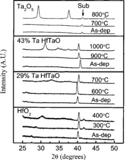
ac-count the poly-Si depletion and quantum-mechanical effects. Figure 1 shows the XRD spectra for HfO2, HfTaO with 29% Ta, HfTaO with 43% Ta, and Ta2O5 as a function of annealing temperatures. The films under examination are of the similar physical thickness共⬃40 nm兲. Except for the as-deposited films, all samples were annealed under the speci-fied temperature by either RTA or furnace annealing(below 600 ° C) in N2 ambient. The annealing times are 30 s for RTA and 30 min for furnace annealing. According to the XRD spectra, the crystallization temperatures of HfO2, HfTaO with 29% Ta, HfTaO with 43% Ta, and Ta2O5 are 400 ° C, 700 ° C, 1000 ° C, and 800 ° C, respectively. Similar crystallization temperatures of pure HfO2共⬃400 °C兲 (Ref. 11) and Ta2O5共⬃700 °C兲 (Ref. 12) have been reported. It is interesting to note that the crystallization temperature of 43% Ta HfTaO film is higher than that of pure HfO2and Ta2O5. This may be attributed to the breaking of the periodic crystal arrangement or the inhibition of continuous crystal growth in gate dielectric by incorporating Ta into HfO2 film.
The high-resolution transmission electron microscopy
(TEM) micrographs of HfO2 and HfTaO with 43% Ta after PDA at 700 ° C for 40 s and activation annealing at 950 ° C for 30 s are shown in Fig. 2. The TEM pictures confirm that the HfO2 film is fully crystallized whereas the HfTaO with 43% Ta film remains amorphous after such annealing. Before annealing, the physical thicknesses of as-deposited HfO2and
43% Ta HfTaO (measured by ellipsometer) are 54.7 and 51.4 Å respectively. After annealing, the physical thick-nesses of HfO2 and HfTaO with 43% Ta films (measured from TEM images) are 41.6 and 37.5 Å, respectively. From the TEM images, the interfacial layers of HfO2 and 43% Ta HfTaO samples are 18.5 and 12.1 Å, respectively. HfTaO with 43% Ta film provides a thinner low- interfacial layer compared to HfO2. This is attributed to the fact that 43% Ta HfTaO remains amorphous after device fabrication. The amorphous layer can effectively block oxygen diffusion through the grain boundaries to form low-interfacial layer during high-temperature annealing.
The C – V characteristic of n+ poly-Si/ HfTaO
共43% Ta兲/p-Si MOS capacitor with EOT of 15 Å is shown
in Fig. 3. The simulated curve with poly-Si depletion and quantum-mechanical corrections is indicated by solid sym-bols. As shown in this figure, the measured C – V curve fits well to the simulated curve, which indicates good interface property between HfTaO and substrate.13Figure 4 shows the corresponding leakage current density–voltage共J–V兲 curve for the sample illustrated in Fig. 3. Compared to SiO2 with same EOT,14the leakage current of HfTaO with 43% Ta film is reduced by two orders of magnitude. As can be seen in the Fig. 4, the leakage current curve exhibits two distinct re-gions, which reflect different conduction mechanisms at low and high bias regions. According to the simulation results, the leakage current is dominated by Frenkel–Poole emission at the low electric-field region. At the high electric-field re-gion, it is believed that the leakage current is dominated by Fowler–Nordheim tunneling.
Boron from the p+ poly-Si gate electrode may easily diffuse not only through the gate dielectric layer, but also into the channel region during dopant activation annealing.
FIG. 1. XRD spectra of HfO2, HfTaO, and Ta2O5 for as-deposited and
different temperature annealing in N2. The crystallization temperature of
HfO2film is increased up to 1000 ° C by incorporating 43% Ta.
FIG. 2. TEM images of HfO2and HfTaO with 43% Ta after PDA at 700 ° C
for 40 s and activation annealing at 950 ° C for 30 s. The HfO2film is fully
crystallized whereas the HfTaO with 43% Ta film remains amorphous.
FIG. 3. C – V characteristic of 43% Ta HfTaO NMOS capacitor with poly-Si gate after activation annealing at 950 ° C for 30 s. The measurement was performed at frequency of 1 MHz and room temperature.
2894 Appl. Phys. Lett., Vol. 85, No. 14, 4 October 2004 Yuet al.
This article is copyrighted as indicated in the article. Reuse of AIP content is subject to the terms at: http://scitation.aip.org/termsconditions. Downloaded to IP: 140.113.38.11 On: Thu, 01 May 2014 04:10:45
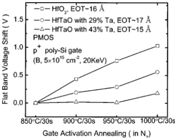
This boron penetration behavior results in interface degrada-tion and flat-band voltage shifts.15 It can be a critical issue for high- gate dielectrics.16Figure 5 shows the monitoring of the flat-band voltage shift as a function of different acti-vation annealing condition in p-type MOS capacitors. The boron penetration-induced flat-band voltage shift in HfO2 film is significantly suppressed by incorporating Ta. The neg-ligible flat-band voltage shift of HfTaO with 43% Ta film is observed up to 950 ° C annealing temperature. The excellent boron penetration immunity of 43% Ta HfTaO is due to its amorphous structure which remains after high-temperature annealing in the device fabrication process.
In summary, both n-type and p-type poly-Si gate MOS capacitors with a HfTaO gate dielectric have been
investi-gated. The incorporation of Ta into HfO2increases the crys-tallization temperature of the film up to 1000 ° C, which can easily withstand the conventional activation annealing at 900– 1000 ° C. Compared to HfO2, a significant reduction in low- interfacial layer growth is observed in the 43% Ta HfTaO film due to its amorphous structure which remains after device fabrication. In addition, boron penetration be-haviors in HfTaO p-type MOS capacitors are sufficiently suppressed as evidenced by the narrow flat-band voltage shift. Consequently, the thermally stable HfTaO gate dielec-tric exhibits good compatibility with conventional poly-Si processes.
This work was supported in part by the Singapore AS-TAR R-263-000-267-305 and in part by Grant No. IME/03-450002.
1
International Technology Roadmap for Semiconductors(Semiconductor
Industry Association, San Jose, CA); http://public.itrs.net/.
2
K. J. Hubbard and D. G. Schlom, J. Mater. Res. 11, 2757(1996).
3
S. H. Bae, C. H. Lee, R. Clark, and D. L. Kwong, IEEE Electron Device Lett. 24, 556(2003).
4
G. D. Wilk, R. M. Wallace, and J. M. Anthony, J. Appl. Phys. 87, 484
(2000).
5
S. Gopalan, K. Onishi, R. Nieh, C. S. Kang, R. Choi, H. J. Cho, S. Krishna, and J. C. Lee, Appl. Phys. Lett. 80, 4416(2002).
6
W. Zhu, T. P. Ma, T. Tamagawa, Y. Di, J. Kim, R. Carruthers, M. Gibso, and T. Furukawa, Tech. Dig. - Int. Electron Devices Meet. 20.4.1(2001).
7
J. H. Lee, Y. S. Kim, H. S. Jung, J. H. Lee, N. I. Lee, H. K. Kang, J. H. Ku, H. S. Kang, Y. K. Kim, K. H. Cho, and K. P. Suh, Tech. Dig. VLSI Symp., 84,(2002).
8
S. Inumiya, K. Sekine, S. Niwa, A. Kaneko, M. Sato, T. Watanabe, H. Fukui, Y. Kamata, M. Koyama, A. Nishiyama, M. Takayanagi, K. Eguchi, and Y. Tsunashima, Tech. Dig. VLSI Symp., 17,(2003).
9
H. S. Jung, Y. S. Kim, J. P. Kim, J. H. Lee, J. H. Lee, N. I. Lee, H. K. Kang, K. P. Suh, H. J. Ryu, C. B. Oh, Y. W. Kim, K. H. Cho, H. S. Baik, Y. S. Chung, H. S. Chang, and D. W. Moon, Tech. Dig. - Int. Electron Devices Meet. 853(2002).
10
G. D. Wilk, R. M. Wallace, and J. M. Anthony, J. Appl. Phys. 89, 5243
(2001).
11
W. J. Zhu, T. Tamagawa, M. Gibson, T. Furukawa, and T. P. Ma, IEEE Electron Device Lett. 23, 649(2002).
12
Y. Matsui, M. Hiratani, I. Asano, and S. Kimura, Tech. Dig. - Int. Electron Devices Meet. 225(2002).
13
C. H. Choi, S. J. Rhee, T. S. Jeon, N. Lu, J. H. Sim, R. Clark, M. Niwa, and D. L. Kwong, Tech. Dig. - Int. Electron Devices Meet. 857(2002).
14
S.-Ho. Lo, D. A. Buchanan, Y. Taur, and W. Wang, IEEE Electron Device Lett. 18, 209(1997).
15
M. A. Quevedo-Lopez, M. El-Bouanani, M. J. Kim, B. E. Gnade, R. M. Wallace, M. R. Visokay, A. Lifatou, M. J. Bevan, and L. Colombo, Appl. Phys. Lett. 81, 1074(2002).
16
H.-J. Cho, D.-G. Park, K.-Y. Lim, J.-K. Ko, I.-S. Yeo, J. W. Park, and J.-S. Roh, Appl. Phys. Lett. 80, 3177(2002).
FIG. 4. Leakage J – V characteristic of HfTaO n-type MOS capacitor with poly-Si gate after activation annealing at 950 ° C for 30 s.
FIG. 5. Comparison of the flat-band voltage shift in HfO2and HfTaO p-type
MOS capacitors after various temperature annealing. HfTaO films show a stronger immunity to boron penetration than HfO2, due to its high
crystal-lization temperature.
Appl. Phys. Lett., Vol. 85, No. 14, 4 October 2004 Yuet al. 2895
This article is copyrighted as indicated in the article. Reuse of AIP content is subject to the terms at: http://scitation.aip.org/termsconditions. Downloaded to IP: 140.113.38.11 On: Thu, 01 May 2014 04:10:45