Fabrication and Characterization of (111)-Oriented and Nanotwinned
Cu by Dc Electrodeposition
Tao-Chi Liu, Chien-Min Liu, Hsiang-Yao Hsiao, Jia-Ling Lu, Yi-Sa Huang, and Chih Chen*
Department of Materials Science & Engineering, National Chiao Tung University, Hsin-chu 30010, Taiwan, R.O.C.
ABSTRACT: We report an approach to fabricating (111)-oriented and nanotwinned Cu (nt-Cu) by dc electroplating. A 200 nm thick Cu with (111) preferred orientation is required as a seed layer. Highly oriented Cufilms with densely packed nanotwins can be grown to exceed 20μm thick at high current and high stirring speeds. X-ray diffraction indicates that the intensity ratio of (111) to (220) is as high as 506, which is the
highest among the reported electroplated Cu films. The
spacing of twins ranges from 10 to 100 nm, which reveals a high hardness value of 2.23 GPa. The (111)-oriented nt-Cu
will have many potential applications in interconnects and 3D IC packaging.
1. INTRODUCTION
Cu has become the most important material for interconnects in back-end-of-line (BEOL) of advanced electronics.1−5Copper possesses a very low electrical resistivity of 1.7μΩ and a very
high thermal conductivity of 401 W m−1 K−1 at room
temperature. Therefore, it replaces Al as the wiring material in very-large-scale integrated (VLSI) devices.2
Furthermore, Cu has been adopted as the major under-bump-metallization (UBM) material in microelectronic pack-aging because of its excellent performance in wettability with solder, high electrical and thermal conductivity.6−8 The thickness of the Cu UBM ranges from 5 to 50μm, and it is also electroplated by direct current (dc).
It is reported that nanotwinned Cu (nt-Cu) can be fabricated using pulsed electroplating.9−12nt-Cu possesses high mechan-ical strength and ductility, while it maintains almost the same conductivity as bulk Cu. nt-Cu also has high electromigration resistance.13 Many researchers also report that nt-Cu can be prepared by pulsed electroplating.14−18 These nt-Cu are all random-oriented. To control the grain orientation of nt-Cu, Zhang employed the magnetron sputtering technique to fabricate nt-Cu with [111] preferred orientation which is normal to growth direction.19However, the deposition rate is very slow and the cost of sputtering is also expensive. The step coverage of sputtering is not good, so it cannot be employed in the damascene process.
Three-dimensional (3D) integrated circuit (IC) integration has recently drawn great attention because it provides solutions to scaling issues of VLSI devices.20,21 Electroplating by dc at high current densities has become very important because Cu needs to be electroplated into through-Si-Vias (TSVs) and the depth of TSVs has to exceed 50μm. In addition, thick Cu is also adopted as the UBM material in microbumps in 3D IC interconnects. Thousands or tens of thousands of microbumps need to be fabricated in a chip. Thus, Cu serves as the most important material for interconnects in 3DIC integration. Abe
et al. reported that (111)-oriented Cu possesses the electro-migration lifetime.22,23 Therefore, (111)-oriented and nano-twinned Cu may be the best structure for resisting electro-migration damage. The design and fabrication of the oriented and nt-Cu are highly intriguing.
We have recently reported a unique method for fabricating (111)-oriented nt-Cu by high stirring rates and high current densities.24However, the details of the electroplating approach have not been revealed. In this paper, we report the fabrication and characterization of the oriented and nt-Cu in detail. In particular, the seed layer plays a critical role in the growth of (111) nt-Cu, which can also be electroplated by dc in patterned openings.
2. EXPERIMENTAL SECTION
A 200 nm thick Ti adhesion layer and a 200 nm thick copper seed layer were sequentially sputtered on a silicon wafer by Oerlikon ClusterLine 300. The Cu seed layer should have a (111) preferred orientation. Electroplating of the nt-Cu can be performed in blanket or patterned Si wafers. For the preparation of patterned Si wafers, a photoresist of 50 μm thickness was applied to the wafer to define arrays of openings with 100μm diameter, and the thickness of the deposited copper is 20μm, which is controlled by current density and operating duration. The electroplating was performed in an anticorrosive PVC container. A high-purity (99.99%) soluble copper anode electrode was put on one side of the container, and the wafer was placed on the other side of the electroplating bath. The distance between cathode and anode was 10 cm. The electroplating bath was high-purity CuSO4 solution composed of 0.8 M copper cations, 40
ppm hydrochloric acid and surfactants. The high concentration of metal ions and the free acid allow electroplating to be operated at high current densities. Chloride ions are used to accelerate copper deposition and modify the crystal texture of Cu. High stirring speeds Received: July 11, 2012
Revised: August 22, 2012 Published: August 30, 2012
of the electrolyte are required for the fabrication of (111) nt-Cu. The stirring can be created by agitating the electrolyte with a stirring magnet. The rotation rate of the holder was set to be 900 rpm, resulting in uniform agitation. The copper metalfilms were deposited at room temperature with varied current densities ranging from 10 mA cm−2to 120 mA cm−2.
The microstructure of the electrodeposited Cu film and patterns were observed with a dual-beam focused ion beam (DB-FIB, FEI 200) and a transmission electron microscope (TEM, Jeol JEM-2100F). The grain orientation was identified using a high-resolution X-ray diffractometer (XRD, BRUKER AXS, D8 Advance X-ray Diffrac-tometer). Electron backscattered diffraction (EBSD, EDAX/TSL Technology) was employed to examine the grain orientation.
3. RESULTS AND DISCUSSION
To grow (111)-oriented nt-Cu, the Cu seed layer needs to possess a strong (111) preferred orientation. Figure 1a shows
the reflections for the X-ray diffraction pattern for the 200 nm thick Cu seed. Niu et al. reported that seed layer can be used to control the crystallographic orientation of noble metals.24,25 The pattern reveals a very strong (111) preferred orientation. Figure 1(b) depicts the cross-sectional TEM image of the Cu seed layer. The Cu grains exhibit columnar structure, and the zone axis is [110], as shown in the corresponding TEM diffraction pattern. The top surface of the grains is the (111) surface. The grains play a critical nucleation role in growing the (111) nt-Cu during the subsequent electroplating process.
Highly oriented (111) grains and densely packed nt-Cufilms can be fabricated at high current densities and high stirring speeds. Figures 2a to 2f show the cross-sectional FIB images for the Cu films deposited at various stirring speeds when the current density wasfixed at 80 mA cm−2. At a low stirring speed
of 100 rpm, random oriented grains grew with few twins. As the stirring speed increased to 200 rpm, some columnar-like grains with parallel twins started to appear, as indicated by the arrows in Figure 2b. Columnar grains of regular twins were observed at 400 rpm, as presented in Figure 2c. The twin density and the regularity of the grains continue to increase with the increase in the stirring speed, as illustrated in Figure 2d to 2f.
The X-ray diffraction indicated that the intensity of the (111) reflection increases with the increase in the stirring speed. Figure 3 shows the X-ray diffraction for the samples in Figure 2. The intensity for the (111) peak increases as the stirring speed increases. The rest of the Cu peaks are all very weak. The X-ray results agree with the FIB images.
The current density also plays a critical role in the growth of the (111)-oriented nt-Cu. Figures 4a to 4f show the cross-sectional FIB images for thefilm deposited at various current densities at 900 rpm. Few oriented nt-Cu grains were grown at
10 mA cm−2. Columnar grains of (111) orientation with
nanotwins grew at 20 mA cm−2, as shown in Figure 4b. The nt-Cu grains become more regular and the twin density increases when the current density increased to 70 mA cm−2. However, the regularity of the nt-Cu decreases with the increasing in the current density after 100 mA cm−2, as shown in Figure 4d to 4f. When the current density reached 120 mA cm−2, the Cu grains without regular nanotwins were grown. The X-ray diffraction in Figure 5 also supports the FIB results. The (111) intensity for the Cufilm at 70 mA cm−2reveals the highest volume among the 6 samples. Therefore, the optimum current density is 70 mA cm−2at 900 rpm for the dc electroplating (111) nt-Cu.
Not only can the (111) nt-Cu be fabricated by dc on blanket Si wafers but also it can be electroplated in patterned openings. Figure 6a presents the tilt-FIB image for a 20μm thick Cu pad
with 100 μm diameter on a Si wafer. FIB etching was
performed at the front edge of the pad to reveal the columnar grains of nt-Cu, as shown in the enlarged FIB image in Figure 6b. Figure 6c shows the plan-view EBSD orientation image map For a Cu pad. The results indicate that almost every surface Figure 1.(a) X-ray diffraction for the sputterred Cu seed layer used in
this study. The seed layer has a strong (111) preferred orientation. (b) Cross-sectional TEM image showing columnar grains in the 200 nm thick Cu seed layer.
Figure 2.Cross-sectional FIB images for the fabricated Cufilm at 80 mA cm−2at (a) 100 rpm; (b) 200 rpm; (c) 400 rpm; (d) 500 rpm; (e) 900 rpm; and (f) 1500 rpm.
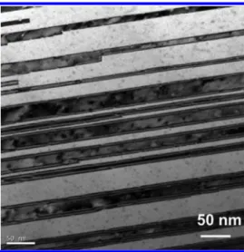
grain is [111] oriented. The average grain size is 3.4± 0.7 μm. Therefore, the (111)-oriented Cu pads can be used as under-bump-metalization to control the orientation of the Cu−Sn intermetallic compounds grown on them.26The electroplated nt-Cu possesses a high density of nanotwins, and it has excellent mechanical properties. Figure 7 shows the cross-sectional TEM images for the (111) nt-Cu deposited by 80 mA cm−2in an opening of 100 μm diameter. The spacing of the
nanotwins ranges from 10 nm to 100 nm, and the average spacing is about 18 nm. With the densely packed nanotwins, the hardness of the nt-Cu becomes higher. Figure 8 shows the Figure 3.(a) X-ray diffraction for the fabricated Cu film in Figure 2.
(b) Plot of (111) intensity vs stirring speed for the six samples in (a).
Figure 4.Microstructures for the Cufilm electroplated at 900 rpm at (a) 10 mA cm−2; (b) 20 mA cm−2; (c) 40 mA cm−2; (d) 70 mA cm−2; (e) 100 mA cm−2; and (f) 120 mA cm−2.
Figure 5.(a) X-ray diffraction for the Cu film grown of the six current densities in Figure 4. (b) Intensity of the Cu (111) peak as a fuction of current density.
Figure 6.(a) FIB tilt-view image showing the fabricated Cu pad with nt-Cu. (b) Enlarged image for the Cu pad at the location processed by FIB ion etching. The thickness of the Cu pad is about 20μm, and the diameter of the pad is 100μm. (c) EBSD orientation image map from the surace of the Cu pad.
typical curve for the hardness measurement from the (111) top surface by nanoindenter at a strain rate of 0.05 mN S−1. The average hardness is obtained by averaging the values from about displacement of about 100 to 300 nm. The average hardness is 2.23± 0.09 GPa and 2.15 ± 0.13 GPa for the nt-Cu deposited at 40 mA cm−2and 80 mA cm−2, respectively. The hardness is in the same order as the random-oriented Cu reported by Lu et al.17 Therefore, the (111)-oriented Cu possesses excellent mechanical properties.
The high stirring rate may create a shear force at the depositing surface. When the Cu cations are going to adhere to the Cufilm at the cathode, they experience a shear force, so that the Cu atoms would displace from faced-centered positions, resulting in the formation of twins. Because the agitation is strong, the displacement of Cu atoms occurs frequently, facilitating the formation of a high density of twins. It is noteworthy that the oriented nt-Cu grains can be grown at suitable current densities ranging from 20 to 100 mA cm−2. At these current densities, most of the Cu atoms can be grown on the (111) Cu seed grains, as illustrated in Figure 2d through 2f. However, when the current density was larger than 120 mA cm−2, the columnar structure cannot be fabricated, as presented in Figure 4. This may be attributed to an increase in the Cu deposition rate as the current density increases. It is speculated that the electroplated Cufilm cannot be grown epitaxially on the Cu seed grains due to the high deposition rate. Nucleation and growth of Cu grain with other orientations may take place. On the other hand, other researchers reported that regular nt-Cu can be fabricated up to 800 mA cm−2.9,27 Yet, they used pulsed electroplating with different seed layers and solutions. Therefore, the optimal current densities may be different from the present work.
Columnar textures in the electrodeposited copper layer usually can be obtained from simple electrodeposition bath with no additives.28 According to the nucleation-coalescence growth mechanism, the columnar textures come from the competing growth among adjacent grains. During the cathodic reduction, the copper cations prefer to be reduced on a low surface energy grain rather than the high energy one. Since the (111) planes are the lowest surface energy plane in fcc crystals, the rapid growth with high current densities specifically increases the grain size along the [111] orientation. Eventually, the (111) columnar grains dominate at a later stage of electroplating.29However, the twin-containing columnar grains have not been obtained in the past by electroplating. This phenomenon can be explained by assuming that the nanotwins reduce the free energy of the Cufilm, because twin boundaries are coherent. Compared with high angle GBs, the TBs are relatively low energy boundaries; the formation of twins is driven for thermodynamically decreasing the total interfacial energy.9,30−32However, the formation mechanism of (111) nt-Cu is not well understood at this moment. It deserves further studies.
Chan et al. reported that increased amount of chloride ions favors (110) Cu texture.14 They reported that the critical chloride concentration was about 40 ppm for dc electroplating without serious agitation, above which (110) Cu texture dominated. Yet, the critical concentration increased to about 60 ppm for pulsed electroplating. The chloride concentration was 40 ppm in the present work. Our highly agitated electroplating is similar to pulsed electroplating. Therefore, it is reasonable that we obtained (111) Cu texture at the concentration of 40 ppm.
Figure 7.Cross-sectional TEM image for the fabricated nt-Cu at 80 mA cm−2at 900 rpm.
Figure 8.The measured hardness vs displacement into surface for the fabricated Cu pad with nt-Cu electroplated at 900 rpm at (a) 40 mA cm−2and (b) 80 mA cm−2. The strain rate is 0.05 mN S−1, and the depth limit is 400 nm.
4. CONCLUSIONS
We successfully fabricated (111)-oriented Cu with a high density of parallel nanotwins by dc electroplating. The oriented nt-Cu can be obtained at a current density ranging from 20 mA cm−2to 100 mA cm−2with a stirring speed over 400 rpm. The nt-Cu has high hardness over 2.0 GPa with a stirring speed over 400 rpm. Most of the surface grains were (111) oriented, which have a low surface diffusion. Therefore, the nt-Cu may have many potential applications as interconnects in microelec-tronics. The nt-Cu can also be electroplated over 20μm thick. Therefore, it can be used as a UBM material to control the growth of the intermetallic compounds. The growth mecha-nism needs further study to have better understanding.
■
AUTHOR INFORMATIONCorresponding Author
*E-mail: chih@mail.nctu.edu.tw.
Notes
The authors declare no competingfinancial interest.
■
ACKNOWLEDGMENTSThe financial support from the National Science Council,
Taiwan, under the Contract NSC 98-2221-E-009-036-MY3 is acknowledged.
■
REFERENCES(1) Hu, C. K.; Harper, J. M. E. Mater. Chem. Phys. 1998, 52, 5. (2) Rosenberg, R. Ann. Rev. Mater. Sci. 2000, 30, 229−262. (3) Thompson, C. V.; Lloyd, J. R. MRS Bull. XVIII 1993, 12, 18. (4) Ho, P. S.; Kwork, T. Rep. Prog. Phys. 1989, 52, 301−348. (5) Edelstein, D. C.; Sai-Halasz, G. A.; Mii, Y. J. IBM J. Res. Dev. 1995, 29, 383.
(6) Kim, H. K.; Liou, H. K.; Tu, K. N. Appl. Phys. Lett. 1995, 66, 2337.
(7) Chen, C.; Tong, H. M.; Tu, K. N. Annu. Rev. Mater. Res. 2010, 40, 531−55.
(8) Worwag, W.; Dory, T. ECTC ’07. Proceedings. 57th; 2007; pp
842−846.
(9) Lu, L.; Shen, Y. F.; Chen, X. H.; Qian, L. H.; Lu, K. Science 2004, 304, 422.
(10) Lu, L.; Chen, X.; Huang, X.; Lu, K. Science 2009, 323, 30. (11) Lu, L.; Sui, M. L.; Lu, K. Science 2000, 287, 1463. (12) Lu, K.; Lu, L.; Suresh, S. Science 2009, 324, 17.
(13) Chen, K. C.; Wu, W. W.; Liao, C. N.; Chen, L. J.; Tu, K. N. J. Appl. Phys. 2010, 108, 066103.
(14) Chan, T. C.; Chueh, Y. L.; Liao, C. N. Cryst. Growth Des. 2011, 11, 4970.
(15) Jang, D.; Cai, C.; Greer, J. R. Nano Lett. 2011, 11, 1743−1746. (16) Xu, L.; Xu, D.; Tu, K. N.; Ca,i, Y.; Wang, N.; Dixit, P.; Pang, J. H. L.; Miao, J. J. Appl. Phys. 2008, 104, 113717.
(17) Lu, L.; Schwaiger, R.; Shan, Z. W.; Dao, M.; Lu, K.; Suresh, S. Acta Mater. 2005, 53, 2169−2179.
(18) Chen, K. C; Wu, W. W; Liao, C. N.; Chen, L. J.; Tu, K. N. Science 2008, 321, 1066.
(19) Zhang, X.; Wang, H.; Chen, X. H.; Lu, L.; Lu, K.; Hoagland, R. G.; Misra, A. Appl. Phys. Lett. 2006, 88, 173116.
(20) Patti, R. S. Proc. IEEE 2006, 94 (6), 1214−1224. (21) Tu, K. N. Microelectron. Reliab. 2011, 51 (3), 517−523. (22) Abe, K.; Harada, Y.; Onoda, H. IEEE Annual International Reliability Physics Symposium, Reno, Nevada; 1998; pp 342−347.
(23) Abe, K.; Harada, Y.; Yoshimaru, M.; Onoda, H. J. Vac. Sci. Technol. 2004, B22 (2), 721−728.
(24) Niua, W.; Guobao, X. Nano Today 2011, 6, 265−285. (25) Niu, W.; Li, Z.-Y.; Shi, L.; Liu, X.; Li, H.; Han, S.; Chen, J.; Xu, Guobao Cryst. Growth. Des. 2008, 8, 4440−4444.
(26) Hsiao, H. Y.; Liu, C. M.; Lin, H. W.; Liu, T. C.; Lu, C. L; Huang, Y. S; Chen, C.; Tu, K. N. Science 2012, 336, 1007−1010.
(27) Jang, D.; Li, X.; Gao, H.; Greer, J. R. Nat. Nanotechnol. 2012, 7 (9), 594−601.
(28) Lowenhein, F. A. Modern Electroplating, 3rd ed.; Wiley: New York, 1974.
(29) Paunovic, M.; Schlesinger, M. Fundamentals of Electrochemical deposition; Wiley: New York, 1998.
(30) Fullman, R. L.; Fisher, J. C. J. Appl. Phys. 1951, 22, 1350−1355. (31) Fullman, R. L. J. Appl. Phys. 1951, 22, 456−460.