國
立
交
通
大
學
光電工程學系顯示科技研究所
碩
士
論
文
基於奈米柱在十二對稱準光子晶體共振腔雷射熱特性
與其電激發結構製程之研究
Thermal Properties of 12-fold Quasi-Photonic Crystal
Microcavity Laser and Developments on its
Electrically-Driven Structure based on Nano-Post
研 究 生:何韋德
指導教授:李柏璁 教授
基於奈米柱在十二對稱準光子晶體共振腔雷射熱
特性與其電激發結構製程之研究
研究生:何韋德
指導教授:李柏璁 教授
國立交通大學顯示科技研究所碩士班
摘
要
電激發與連續性操作是目前光子晶體共振腔雷射所需解決的兩個重大課題。在本 論文中,為了達到以上兩個目的,我們設計了結合奈米柱結構且具有耳語廊模態之電 激發十二對稱準光子晶體共振腔雷射。在本論文中,我們首先用有效元素分析法模擬 在不同奈米柱大小與傾斜度下之熱傳導行為,並探討受奈米柱結構影響下熱特性之改 善。我們並針對奈米柱大小在不同的半徑晶格常數比與空氣孔洞半徑下之製程作探 討。此外,藉由分析在不同基板溫度與工作週期下之量測結果,我們發現越大的奈米 柱體積擁有越好的散射效果,而此一結果充分證實了奈米柱結構具有可連續性操作之 潛力。 此外,我們成功製作出奈米柱結構電激發光子晶體共振腔雷射,並解決了許多製 程中所遇到的困難,如大面積柱狀平台之製程、如何將光子晶體定義在柱狀平台上、 最後的奈米柱製程等。在量測方面,我們探討了元件的基本電性,及光激光譜和電激 光譜間的比較。而最後我們在波長 1526 nm 與 1545nm 處觀察到了電激發光之耳語廊 模態共振行為。
ii
Thermal Properties of 12-Fold Quasi-Photonic Crystal
Microcavity Laser and Developments on its Electrically-Driven
Structure based on Nano-Post
student:Wei-De Ho
Advisors:Prof. Po-Tsung Lee
Department of Photonics, Display Institute
National Chiao Tung University
Abstract
Electrically-driven and continuous-wave operation are two challenge to photonic crystal microcavity laser, in this thesis, we design 12-fold quasi-photonic crystal microcavity on the nano-post structure with whispering-gallery mode. First, we use finite element method to simulate the heat transfer behavior of nano-post structure with different nano-post sizes and post tilted angles to investigate the thermal properties improvement by nano-post. In fabrication, we can control the nano-post size with respect to different r / a ratio and air-hole radius. Also, by measurement results with different substrate temperature and pump duty cycle, we find the larger post volume will provide better thermal properties, and it can verify the potential of nano-post structure in continuous-wave operation.
Additionally, we have finished the fabrication processes of electrically-driven 12-fold QPC D2 microcavity and solved many problems in fabrication, such as the large post
formation with PR filling, 12-fold quasi-photonic crystal microcavity pattern definition, nano-post formation with appropriate size, etc. In the measurement, we investigate the basic
electrical properties of this structure. Besides, the electro-luminescence and photo-luminescence spectra of device are obtained and compared with each other. Finally, the electro-luminescence of whispering-gallery mode resonance at 1526 and 1545 nm are observed based on this nano-post structure.
iv
Acknowledgements
在這兩年的時間裡,所學到真的東西真的很多,不同於以往書本上的知識探討, 更多的是要自己動手去設計實驗、操作儀器、反覆的從失敗中吸取經驗找出最後所要 的解答。首先我要感謝我的父母親對我的栽培,讓我有機會可以進入研究所來學習與 作研究。再來要謝謝在這個期間裡一直陪伴我的女朋友彬彬,不論是在實驗上成功往 前邁進時和我一起分享喜悅,或遇到瓶頸深陷泥淖時給我支持與鼓勵,都給了我很多 繼續向前的動力。 然而更多要感謝的是我實驗室遇到的夥伴及指導教授。我很感激我的指導老師李 柏璁教授,她在實驗上給我的指點與開導讓我知道自己該改進方向與目標。從一開始 作實驗就引領著我的博士班學長盧贊文,大至分析實驗上遇到困難可能的原因以及一 起討論實驗的結果,小至會議期刊文章的撰寫及上台發表的技巧,我都從他身上學到 了很多,我相當感謝他這麼認真的指導我。並且我也要謝謝帶我的碩士班學長老漢, 不僅是在機台管理上的教導,或是在實驗題目上的指點,以及各個模擬繪圖軟體的操 作,都是由他傳承給我的。再來要謝謝的是我的戰友蕭逸華,除了幫我寫 E-beam、拍 SEM 以外,一同參加 OPT 和 CLEO,一起在實驗上學習成長,有這樣一個戰友的互相 砥礪讓我能夠更順利的解決各個難關。另外要謝謝和我一起管理 ICP 的張家豪也幫了 我很多,除了一起解決機台各種惱人的疑難雜症,也在實驗上鍍電極的部分幫了很大 的忙。此外,我也要感謝同屆的李欣育、林怡先、洪青樺等同學也陪伴我度過了這兩 年的時光,還有學弟林品佐和蕭君源給我的幫助讓我更順利完成我的實驗。要感謝的 人非常的多,如果沒有以上這些人的幫忙,我的實驗以及這本論文便無法如此順利完 成,真的很感謝你們。 2009 年 7 月
Table of Contents
Abstract (in Chinese) ……….……… i Abstract (in English) ……….……… ii Acknowledgements ……….……… iv Table of Contents ……….……… V Table Captions ……….……… Vii Figure Captions ……….……… viii Chapter 1 Introduction……….... 1 1.1 Photonic crystal microcavity lasers……… 1 1.2 Motivation……….. 5 1.3 Overview……….. 8 Chapter 2 12‐fold QPC microcavity for electrically‐driven structure with different central post sizes………. 9 2.1 Introduction……….. 9 2.2 Thermal properties simulation by Finite Element Method and electrical resistance calculation……… 10 2.2.1 Finite Element Method………. 10 2.2.2 Simulation of thermal properties with different post sizes... 13 2.2.3 Simulation of thermal properties and electrical resistance calculation with different post tilted angles……… 14 2.3 Fabrication and post‐size controlling………. 16 2.4 Measurement results………... 19 2.4.1 Measurement setup……… 19 2.4.2 Lasing Properties……….. 20 2.4.3 Measurement with different substrate temperature……….. 22 2.5 Conclusion……… 27 Chapter 3 Realization of electrically‐driven Photonic crystal microcavity laser……. 28 3.1 Introduction………. 28 3.2 Fabrication processes……… 28 3.2.1 Fabrication processes of mesa structure………. 32 3.2.1.1 Photolithography first time and ICP dry‐etching...………. 32
vi 3.2.1.2 Undercut first time……… 35 3.2.1.3 Fill with PR and Remnant PR Clean……… 40 3.2.1.4 Photolithography second time and Electrode deposited……… 41 3.2.2 Fabrication Processes of Photonic Crystal Pattern……… 43 3.2.2.1 Define Pattern by E‐beam Lithography……….. 43 3.2.2.2 ICP Dry‐Etching………..………. 43 3.2.2.3 Undercut Second Time……… 45 3.3 Electro‐Luminescence Measurement………. 48 3.3.1 Setup………. 48 3.3.2 Measurement………. 50 3.4 Conclusion………. 53 Chapter 4 Conclusion & Future Work……… 55 Reference……… 57
Table Captions
Chapter 2
Table. 2. 1: The coefficients for different materials in the simulations. (in M. K. S. unit) 11viii
Figure Captions
Chapter 1
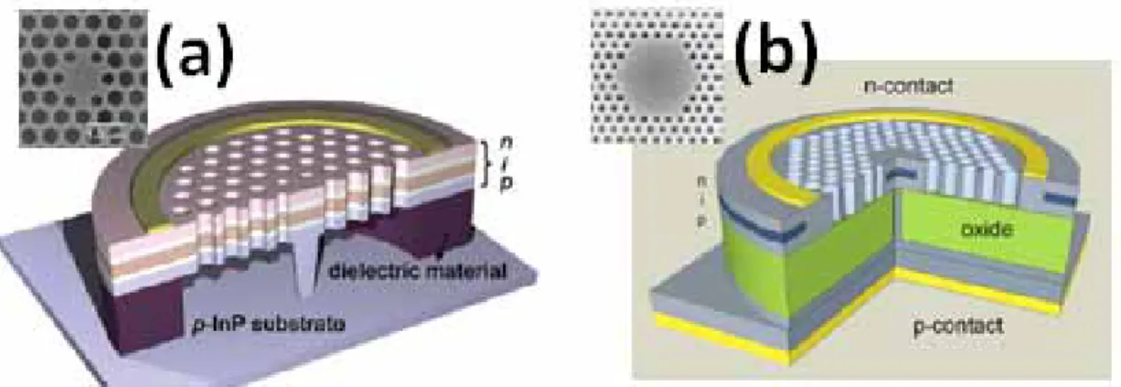
Fig. 1. 1: Fig. 1. 2: Fig. 1. 3: The scheme of 1D, 2D, and 3D photonic crystal. The scheme of photonic crystal composed by (a) dielectric rods and (b) air‐holes on slab structure. The scheme of photonic crystal with (a) triangular and (b) square lattice structure. 1 2 3Fig. 1. 4: The PBG gap map of square and triangular lattice photonic crystal. ( Adopted from reference [8] ) 3 Fig. 1. 5: Photonic crystal microcavity formed by numbers of air holes on dielectric 4 slab with introduced defect to be cavity. ( Adopted from reference [15] ) Fig. 1. 6: Scheme of electrically‐driven structure with photonic crystal pattern in 6 the inset was achieved by (a) prof. Y. H Lee’s group (b) prof. K. D. Choquette’s group, they fabricate the post structure by wet‐etching and oxidation, respectively. ( Adopted from reference [20] [23] )
Fig. 1. 7: The mode profile of whispering‐gallery (WG) mode in micro‐disk. 7
Fig. 1. 8: (a) the 12‐fold quasi‐photonic crystal (QPC) D2 microcavity with seven 7
missing air holes in the cavity center and (b) the inserted appropriate‐size central post under the cavity region.
Chapter 2
Fig. 2. 1: Fig. 2. 2:Scheme of one‐six domain of 12‐fold QPC D2 microcavity in the FEM
simulation setup. The air‐cladding thickness, lattice constant, r/a ratio, and slab thickness are set to be 2 μm, 520 nm, 0.34, and 220 nm, respectively.
(a) The simulated temperature distributions and (b) decay curves of 13
Fig. 2. 3: Fig. 2. 4: Fig. 2. 5: Fig. 2. 6: Fig. 2. 7: Fig. 2. 8: Fig. 2. 9: microcavities with D = 0, 400, 600, and 800 nm. (a) The simulated temperature distributions of microcavity with D = 800 nm post and tilted angles of 60°, 75°, and 90°. The plots of (b) highest temperature and (c) temperature decay time versus the post tilted angle. The illustration of fabrication processes.
(a) Top and (b) tilted‐view SEM pictures of fabricated microcavity with central post
(a) The plot of the effective post size versus wet‐etching time when the
r/a rato is 0.37. (b) The plot of the effective post size versus the air‐hole
radius when the wet‐etching time is 130 seconds. (c) Top‐view SEM pictures of microcavities with D = 480, 650, and 900 nm
The illustration of micro‐PL measurement system with temperature controlling system.
(a) The measured lasing spectra above and below threshold at wavelength of 1485 nm. The measured spectral line width near threshold is 0.18 nm by Lorentzian fitting. (b) L‐L curve of 12‐fold QPhC D2 microcavity with nano‐post size D of 830 nm. The threshold is
estimated to be 0.6 mW and the SEM picture of measured device is also shown in the inset.
The lasing spectra of 12‐fold QPhC D2 microcavity from (a) WG6, 1 and
(b) WG3, 2 mode at 1470 and 1410 nm, with D = 700, 1100 nm 15 17 18 19 20 21 22 Fig. 2. 10: (a) L‐L curves of microcavity with nano‐post size D = 830 nm under 23 substrate temperatures of 20, 35, 50, 60, and 70 °C, respectively. (b) The relationship between the threshold and the substrate temperature. Fig. 2. 11: The lasing wavelength variation plot when the substrate temperature is 24 varied from 20 to 70 °C. The red‐shift rate is about 0.050 nm / °C, which is smaller than that (0.086 nm / °C) of microcavity without nano‐post beneath.
x Fig. 2. 12: (a) L‐L curves of microcavity with nano‐post beneath under different 25 pump duty cycles from 0.5 to 16.0 %. (b) The relationships of the pump duty cycle versus the spectral line width and the threshold. Both spectral line width and threshold increase with the increasing pump duty cycle.
Fig. 2. 13: The measured WG6, 1 mode spectra near threshold when the pump 26
duty cycles are 0.5, 2.0, 4.0, and 8.0 %. The spectral line width is broadened due to the increasing thermal effect from the increased pump duty cycle.
Chapter 3
Fig. 3. 1: Fig. 3. 2: Fig. 3. 3: Fig. 3. 4: Fig. 3. 5: Fig. 3. 6: Fig. 3. 7:Illustration of the device structure after (a) mesa structure formation process and (b) photonic crystal pattern. (c) The wafer structure of electrically‐driven photonic crystal microcavity. The fabrication processes of mesa structure. The fabrication processes of photonic crystal pattern Fig. 3. 4: Photo mask design of mesa (40、50、60 μm in diameter) and electrode (10μm). The tilted and cross‐section SEM picture of the (a) (b) too large post size and (c) (d) too small post size. The remnant PR on the top of these SEM pictures have been cleaned in the following step. The (a) tilted and (b) cross‐section SEM picture of the sample filled with PR under MQWs slab successfully with appropriate post size. And the remnant PR on the top of these SEM pictures have been cleaned in the following step. The tilted and cross‐section SEM picture of 50μm‐diameter‐mesa filled with PR under MQWs slab ,and the post size and height of PR are 33.3 μm and 450 nm for wet‐etching time of 85 second (a) (b) , 28 μm and 334 nm for wet‐etching time of 90 second (c) (d). And the remnant PR 29 31 32 34 36 37 38
Fig. 3. 8: Fig. 3. 9: Fig. 3. 10: Fig. 3. 11: Fig. 3. 12: Fig. 3 .13: Fig. 3. 14: Fig. 3. 15:
on the top of these SEM pictures have been cleaned in the following step. The tilted and cross‐section SEM picture of 40μm‐diameter‐mesa filled with PR under MQWs slab ,and the post size and height of PR are 24.6 μm and 771 nm for wet‐etching time of 60 second (a) (b) , 21.6 μm and 750 nm for wet‐etching time of 65 second (c) (d), 17.1 μm and 253 nm for wet‐etching time of 70 second (e) (f). And the remnant PR on the top of these SEM pictures have been cleaned in the following step. The tilted SEM picture with O2 plasma of (a) 2 min and (b) 3 min. The former is still with few PR, and the later is cleaned clearly. (a) (b) The SEM pictures of mesa structure successfully fabricated with ring‐shape Au/Ge/Ni metal contact.
The measured I‐V curve of device (a) with PR and (b) without PR, the turn‐on voltage of each are 4.51 V and 3.88 V, and the resistance of each are 487.6 Ω and 549.8 Ω, respectively.
The measured PL spectra of (a) original sample (unprocessed), (b) mesa with PR and (c) without PR, with intensity of emission peak of 826.4, 672.2, and 569 pW, respectively. Top view SEM pictures of mesa with PR after pattern defining and dry‐etching (left) and the 12‐fold D2 quasi‐photonic crystal pattern (right).
Top view SEM pictures of device without undercut after pattern defining and dry‐etching (left) and the 12‐fold D2 quasi‐photonic crystal
pattern (right).
(a) The top‐view SEM picture of the complete device of electrically‐driven photonic crystal microcavity. (b) 12‐fold D2
quasi‐photonic crystal microcavity pattern with central nano‐post. (c) The effective post size is estimated to be 776 nm, satisfying the post size condition (< 830 nm) for WG6.1 mode. (d) The tilted 45° SEM picture of
cavity, the bottom of nano‐post is observed from air hole nearest to 39 40 41 42 42 44 44 46
xii Fig. 3. 16: Fig. 3. 17: Fig. 3. 18: Fig. 3. 19: Fig. 3. 20: Fig. 3. 21: cavity.
(a) The top‐view SEM picture of device without PR filling of electrically‐driven photonic crystal microcavity. (b) 12‐fold D2
quasi‐photonic crystal microcavity pattern with central nano‐post. (c) The effective post size is estimated to be 666 nm, satisfying the post size condition(< 830 nm) for WG6.1 mode. (d) (e) Top‐ and tilted‐view of
12‐fold D2 quasi‐photonic crystal microcavity pattern with larger central
nano‐post of 1340nm. (f) The tilted 45° SEM picture of cavity, the bottom of nano‐post is observed from air hole nearst to cavity. The measured I‐V curve of device (a) with PR and (b) without PR after wet‐etching process with nano‐post (D~900 nm), the turn‐on voltage of each are 4.23 V and 4.76 V, and the resistance of each are 813.3 Ω and 594.6 Ω, respectively. The illustration and pictures of our micro‐EL measurement system
The picture of probing contact on PR‐filled mesa with and without photonic crystal pattern from CCD monitor. The measured EL spectra of device (a) with PR and (b) without PR with respect to different input voltage. Fig. 3. 21 : The measured EL spectra (a) with resonance modes at 1526 and 1545 m with D ~ 1000 nm from device without PR, which is corresponding to WG5, 1 and WG4, 1 modes by FDTD simulation, and (b)
without resonance from device with PR, gain peak of 1546 nm. 47 48 49 51 51 53
Fig. 3. 22: The lasing spectra under optical‐pumping of 12‐fold QPhC D2 microcavity 53
from (a) WG6, 1 and (b) WG3, 2 mode at 1412 and 1367 nm, with D = 600,
1000 nm, respectively.
Chapter 1 Introduction
1.1 Photonic Crystal Microcavity Lasers
Photonic crystal is an artificial multidimensional periodic structure with different refractive indices that can affect the propagation of electromagnetic waves, such as electrons motion affected in semiconductor crystal, or even confine electromagnetic waves in some region. It was first proposed by E.Yablonovitch in 1987 [1]. There are many characteristics similar to semiconductor crystal, such as bands of photons, air band, dielectric band, and photonic badgap.(contrast with bands of electrons, conduction band, valence band, and electronic bandgap) The most important one is photonic bandgap, which is a forbidden gap for photons. Light can not enter this region, which is the same as electrons can not pass through the electronic bandgap. In other words photonic band gap is an insulator of light. According to the dimensions of periodic structure, photonic crystal can be classified into one dimension (1D), two dimension (2D), and three dimension (3D), as shown in Fig. 1. 1.
2
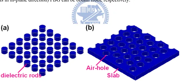
This 1D photonic crystal is proposed by William H. Bragg, which is known as distributed Bragg reflector (DBR). It is a high quality reflector that can almost forbid light in the direction the dielectric medium arranged, and widely used in semiconductor lasers and waveguides. Both 2D and 3D photonic crystal can achieve large photonic bandgap, but 3D is more difficult in fabrication. Take it into consideration, 2D photonic crystal was researched by many people, and widely employed in various applications lately, for example, light emitting diode (LED) [2], semiconductor lasers [3], waveguides, fibers [4] , etc. Generally speaking, 2D photonic crystal can be classified into two types of air holes on dielectric slab and dielectric rods structures, as shown in Fig. 1. 2, which TE (transverse electric, the electric field is in in-plane direction) and TM (transverse magnetic the magnetic field is in in-plane direction) PBG can be obtain from, respectively.
Fig. 1. 2: The scheme of photonic crystal composed by (a) dielectric rods and (b) air-holes on slab structure.
The square and triangular lattice are two basic specimens with low symmetry, as shown in Fig. 1. 3. And we can obtain large PBG in TE- and TM- like modes from these two lattices for certain designs, as shown in Fig. 1. 4. Recently, something different like quasi-photonic crystal with high symmetry are reported, such as
octagonal [5] , dodecagonal [6] ,and circular photonic crystal [7] , and large bandgap can also be obtained.
Fig. 1. 3: The scheme of photonic crystal with (a) triangular and (b) square lattice structure.
Fig. 1. 4: The PBG gap map of square and triangular lattice photonic crystal. ( Adopted from reference [8] )
By PBG effect, we can reflect all in-plane light within some specified frequency in the photonic crystal. It’s a powerful and useful property. For example, we can introduce a point defect to design a microcavity, or a line defect to make a waveguide. Here, we take microcavity for discussion. A typical photonic crystal microcavity is usually formed by numbers of air holes on dielectric slab with introduced defect in
4
freestanding structure, as shown in Fig. 1. 5. Light is localized, and then resonate in the cavity region by two mechanism, in-plane direction confined by photonic crystal and vertical confined by total internal reflection (TIR). To control the modal properties, we modify the lattice constant (a) or air hole versus lattice constant (r/a) ratio, then we can change the wavelength of localized modes and PBG region. Moreover, by change the cavity pattern design, photonic crystal microcavities with lots of excellent optical properties are reported, such as ultra high quality (Q) factor [9] [10] , extreme small mode volume [11] [12] , ultra low threshold [13] , high coupling effect with waveguide [14] , and so on.
Fig. 1. 5 : Photonic crystal microcavity formed by numbers of air holes on dielectric slab with introduced defect to be cavity. ( Adopted from reference [15] )
Though numerous great properties are investigated and reported, there are still some problems need to be solved, and more and more group take notice of it. First, most photonic crystal microcavities are optical pumping, an electrically-driven structure for photonic crystal microcavites is difficult to fabricate but benefit for making it practical. Second, continuous wave (CW) lasing is not easy to achieve due
to poor heat dissipation property of membrane structure. Thus, if we can make device in electrically pumping as well as CW condition, it will do good to photonic crystal microcavity in research and application a lot.
In this thesis, I will focus on solving these two problems and realize the electrically-driven structure for photonic crystal microcavity and also operated with good thermal properties.
1.2 Motivation
Photonic crystal (PhC) microcavity lasers with high quality (Q) factor and small mode volume have been achieved and reported [9-12]. And it can be served as high efficiency and low threshold light sources that will benefit for photonic integrated circuits and quantum electro-dynamics applications. Nevertheless, most of the great reports are operated by optical pumping. In order to promote these devices to practical applications, such as photonic integrated circuit, optical communication system , and biological sensors, etc, a robust, applicable, and practical electrically-driven structure is necessary and important. From past researches, the concept of inserted a central post under microcavity [16] [17] , originated from micro-disks [18] [19] , has been regarded as a promising way to achieve electrically-driven photonic crystal micorcavity lasers. The post can not only be a current pathway but also a heat sinker and a mode selector.
Very recently, the electrically-driven photonic crystal microcavity lasers with lasing action of monopole mode [20] [21] , and hexapole mode [22] are first
6
demonstrated and reported upon this central post structure by Prof. Y. H Lee’s group, they fabricate the post structure by wet-etching, as shown in Fig. 1. 6 (a). And there are still other groups research on this topic, such as Prof. K. D. Choquette’s group [23], they fabricate the post by oxidation, as shown in Fig. 1. 6 (b).
Fig. 1. 6 : Scheme of electrically-driven structure with photonic crystal pattern in the inset was achieved by (a) Prof. Y. H Lee’s group (b) Prof. K. D. Choquette’s group, they fabricate the post structure by wet-etching and oxidation, respectively. ( Adopted from reference [20] [23] )
Among various modes ,we think the whispering-gallery (WG) mode would be a good candidate for this central post structure due to its central zero field distribution that the mode profile dose not overlap the post region spatially, as shown in Fig. 1. 7 . Thus, high Q factor due to small perturbation by post, and relative small mode volume compared with the microcavity size can be obtained. Here, we adopt the 12-fold quasi-photonic crystal (QPC) D2 microcavity with seven missing air holes in the
cavity center due to its high Q-factor WG mode and large photonic band gap , as shown in Fig. 1. 8 (a). Then we insert an appropriate size central post under the cavity region will not disturb the mode profile, and let it be a current pathway, as shown in Fig 1. 8 (b) .
Fig. 1. 7 : The mode profile of whispering-gallery (WG) mode in micro-disk.
Fig. 1. 8 : (a) the 12-fold quasi-photonic crystal (QPC) D2 microcavity with seven
missing air holes in the cavity center and (b) the inserted appropriate-size central post under the cavity region.
In our previous research [6] , we have investigated the mode behavior in 12-fold QPC D2 microcavity with different post sizes, and obtained high measured Q factor of
8,400 from WG6, 1 (the former and latter sub-numbers denote the azimuthal number
and radial order of the WG mode) mode with effective post size 420 nm in diameter. We also emphasize the better thermal and electrical properties for microcavity with large central post (post size < 830 nm in diameter). The larger central post should lead
8
lower electrical resistance and better heat sinking, but it may make Q factor degrade. It is exactly a trade-off between Q-factor and above thermal and electrical properties. We will investigate these effects in detail from simulation, fabrication, and measurement in later chapters. By introducing the 12-fold QPC D2 microcavity with
appropriate size central post based on WG6, 1 mode, the continuous-wave
electrically-driven microcavity laser can be expected to be achieved with high Q, low threshold, and better thermal effect.
1.3 Overview
In this thesis, in chapter 2, we will investigate the thermal properties improvement induced by central post by using finite-element method (FEM) . Also, we can control the post size by fine-tuning the wet-etching time. Besides, we discuss the measurement results about modal properties and thermal properties improvement by changing the substrate temperature and pump duty cycle. In chapter 3, the photonic crystal microcavity on electrically-driven structure is realized, and the fabrication process of device will be illustrated in detail. We will discuss about the difficulties we meet in fabrication and the way we used to solve the problems. Then we will show the EL measurement results of photonic crystal microcavity by electrically driving. Finally, we will do a brief conclusion in Chapter 4.
Chapter 2 12-Fold QPC Microcavity
for Electrically-Driven Structure with
Different Central Post Sizes
2.1 Introduction
In this chapter, we focus our researches on the thermal properties improvement
of 12-fold QPC microcavity due to central post. At first, we simulate the thermal properties of microcavities with different post sizes and shapes by finite-element method (FEM) ; besides, we also calculate the electrical resistance with respect to different post sizes and shapes to compare the electrically properties applied for electrically-pumping. Then, we investigate the fabrication of 12-fold quasi-photonic crystal microcavity with size-controlled central post for electrically-driven structure by fine-tuning the wet-etching time. From the real devices, we measure the WG6, 1
mode lasing and its thermal properties from microcavities with appropriate size central posts by varying the substrate temperature and duty cycle, and verify the better heat dissipation than that of 12-fold QPhC membrane microcavity.
Besides, CW lasing is difficult to achieve in membrane structure due to the poor heat dissipation of the air-cladding; however, we can observe the lasing action in large duty cycle from real devices with central post because the higher thermal conductivity of dielectric. It strongly indicate that the probability of CW lasing , and we will discuss about this issue in this chapter from FEM simulation and measurement results.
10
2.2 Thermal properties simulation by Finite Element
Method and electrical resistance calculation
2.2.1 Finite Element Method and Simulation Setup
The finite element method (FEM) is a numerical technique for finding approximate solutions of partial differential equations (PDE) as well as of integral equations. It was proposed by Richard Courant (1942) . The purpose of FEM is to find the steady state of a system by employing variational method, and it can solve the boundary value problem and eigen-value problem. To apply this method, it requires discretization of a continuous domain into a set of discrete sub-domains, usually called elements, and the solution of each element would be approximated by certain characteristic form to solve the problems.
Here we will use FEM to calculate heat dissipation of different post size of 12-fold QPC D2 microcavity. During the simulations, we find the heat radiation and
convection are relatively low compared with heat conduction, that is mean the heat conduction will dominate the heat transfer behavior [24] . The general conductive heat transfer equation is given by:
H
T
k
t
T
C
p+
∇
⋅
−
∇
=
∂
∂
(
)
ρ
(1)where ρ, Cp, T, k, and H are denote the density of material, heat capacity of material, temperature, thermal conductivity of material, and the given heat sources,
respectively. And the coefficients for different materials in the simulation are shown in Table. 2. 1. k (Thermal Conductivity) (W/m‧K) ρ(Density) (kg/m3) Cp(Heat Capacity ) (J/kg‧K) Air 0.025 1.205 1006 InGaAsP 39.871 5445.16 282.26 InP 68 4810 310
Table. 2. 1: The coefficients for different materials in the simulations. (in M. K. S. unit)
The H denotes a time- and position-dependaent surface heat source is given by the equation (2). The part A of eq. (2) denotes the region of heat sources, in this case, a circular region with radius of 0.88 µm. The part B is the duration time of the heat source, in this case, a pulse with 25 ns. And the part C is heat energy which is calculated by the equation (3), where W, S and E is pumping energy, pumping area and energy per m3. The term D means that the electro-magnetic wave transmits to the dielectric material and is absorbed by the material, that is, the energy skin depth related to the absorption coefficient of the material α (for InP, α = 3.5×10⁶). Besides, the position of the heat source is also given in term D, in this case, at the surface.
z) 10 (2.2 ) 10 3.5 ( exp ) 10 25 (t ) 10 8.798 ) y (x2+ 2 0.5< ⋅ −7 ⋅ < ⋅ −9 ⋅E⋅ − ⋅ 6 ⋅ ⋅ −7− (2) A B C D
12
E
S
W
⋅
α
=
⋅
π
(3)The simulation setup and scheme of 12-fold QPC D2 microcavity membrane
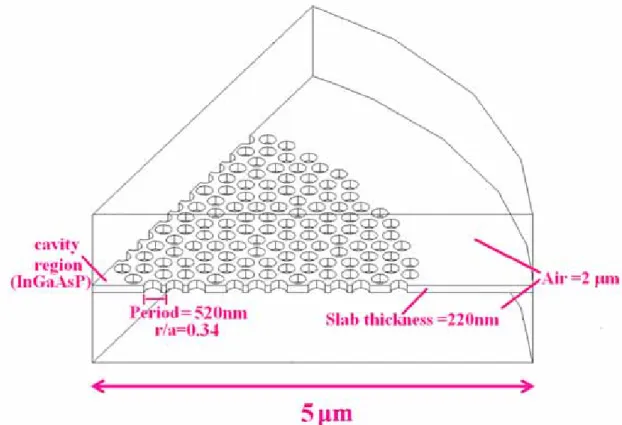
structure formed by Air / InGaAsP / Air is illustrated in Fig. 2. 1 The lattice constant, r/a ratio, and slab thickness are set to be 520 nm, 0.34, and 220 nm respectively. The simulation domain is a circle with 11 µm radius in x-y plane and the air cladding thickness in z-direction is set to be 2 µm. The simulation time is set to be 400ns, which is limited by our computer capability. Besides, to accelerate the simulations and save the computer memory, we reduce the simulation time domain into one-sixth of the whole structure due to the lattice symmetry. And the boundary conditions we set are thermal insulation and axial symmetry [25] . The thermal insulation means that the quantity of in- and out-ward heat sources passing equally through the surface. The initial temperature of the simulation domain is 300k, the boundary will be treated as the cooling source. In our simulation setup, the top, bottom, and the back boundaries are set to be thermal insulation. And the side boundaries are set to be axial symmetry.
Fig. 2. 1 Scheme of one-six domain of 12-fold QPC D2 microcavity in the FEM
simulation setup. The air-cladding thickness, lattice constant, r/a ratio, and slab thickness are set to be 2 µm, 520 nm, 0.34, and 220 nm, respectively.
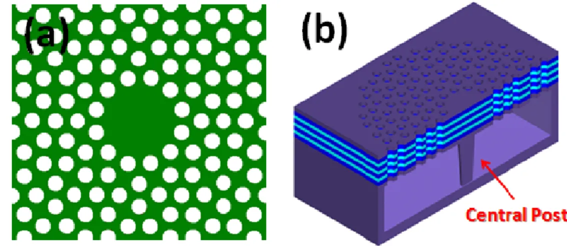
2.2.2 Simulation of Thermal Properties with Different Post Sizes
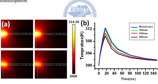
The thermal conductivity of air and InP are 0.025 and 68 W/(m·k), respectively. Obviously, the thermal transfer ability of InP is much more superior to air. To investigate the heat-sinking ability of central post, we use FEM to simulate the heat transfer behaviors of micocavities with different central post sizes. Here, we define the effective post size, D, as two times the distance from cavity center to outmost position of the post. The simulated temprature distributions and their decay curves of the microcavities with different D of 0 (membrane), 400, 600, and 800 nm in diameter are shown in Fig. 2. 2 (a) and (b), The highest temperature and decay time are 312.4, 311.8, 310.6, and 309.7 K and 25.3, 25.2, 22.4,and 20 ns, respectively, when D is
14
varied from 0, 400, 600 to 800 nm. The decay time is defined as the time duration for the temperature drop to 1/e of its highest value by first order exponential fitting. From Fig. 2. 2, we can see clearly both the highest temperature and decay time of the microcavities are declined substantially.
As we mentioned before, there is a trade-off between Q factor and heat-sinking. And in our previous research, the post is appropriate small than 830 nm in diameter [6] . With the simulation results, the post of 830 nm in diameter would be a better design in this structure that has excellent thermal dissipation and no significantly Q-factor degradation, too. Above simulated heat transfer behaviors directly indicate that the nano-post beneath the microcavity can provide extra heat sink and improve heatdissipation.
Fig. 2. 2: (a) The simulated temperature distributions and (b) decay curves of microcavities with D = 0, 400, 600, and 800 nm.
2.2.3 Simulation of Thermal Properties and Electrical Resistance
Calculation with Different Post Tilted Angles
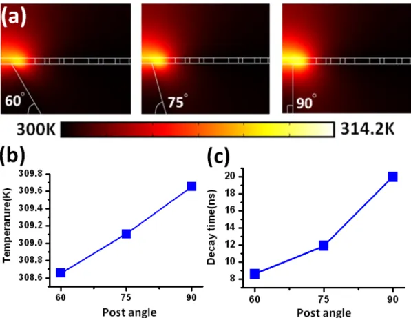
From the real devices, we find the fabricated post under microcavity is cone-shaped instead of a cylinder. The SEM picture is shown in next section. That means the post volume will be larger than the cylinder post with the same interface connected to the membrane, which could conduct more heat energy. Thus, we simulate the heat transiton behaviors of microcavity with central post of D = 800 nm and tilted angles of 60°, 75° and 90°. The simulated temprature distributions is shown in Fig. 2. 3(a). And the simulated highest temperatures and their decay times of post tilted angles of 90°, 75°, and 60° are 309.7, 309.1, and 308.7 K and 20.0, 11.9, and 8.6 ns, respectively, as shown in Fig. 2. 3(b) and (c).
Fig. 2. 3: (a) The simulated temperature distributions of microcavity with D = 800 nm post and tilted angles of 60°, 75°, and 90°. The plots of (b) highest temperature and (c) temperature decay time versus the post tilted angle.
16
From Fig. 2. 4, we find that in spite of the highest temperature only decrease 1K, from 309.7K to 308.7K, however, the decay time of microcavity decline drastically in duration of 11.4 ns. The decay time is the certain index of heat-sinking, because of transmitting heat fast, the Q factor of microcavity could not degrade a lot from more heat accumulation. And we can get even better effect of post in thermal properties improvement due to the actual cone-shaped post in contrast with our past research results [6] .
To investigate the electrical property variation from cone-shaped post, we also calculate the electrical resistance by this formula:
R = ρ × ( L / A ) (4)
, where R, ρ, L, and A represent the electric resistance, resistivity, height, and effective area of the post, respectively. The ρ and L of heavily Zn-doped (~1018 cm-3) InP post are 0.0417 Ω·cm and 800 nm, respectively. The calculated R of post with D = 800 nm with tilted angles of 60°, 75°, and 90° are 370, 621, and 1043 Ω, respectively. Obviously, the larger central post volume will lead to lower electric resistance, which is benefit in reducing the carrier non-radiative recombination in electrical-driving.
2.3 Fabrication and Post-Size Controlling
The D2 microcavity is defined by removing seven air-holes on a thin dielectric
membrane with thickness and refrective index of 220 nm and 3.4. The fabrication process starts from drawing QPhC patterns by electron-beam lithography on
polymethylmethacrylate on epitaxial structure consisting of compressively strained InGaAsP multi-quantum-wells (MQWs). And then transfering the QPhC patterns into MQWs by a series of inductively coupled plasma and reactive ion dry etching processes. Finally, the InP substrate is open up and the membrane microcavity with a central post beneath is achieved by HCl : H2O = 3 : 1 selective wet-etching process.
The illustration of fabrication processes is shown in Fig. 2. 4. Top- and tilted-view scanning-electron-microscope (SEM) pictures of fabricated 12-fold QPhC D2
microcavity with central post are shown in Fig. 2. 5 (a) and (b).
18
Fig. 2. 5: (a) Top and (b) tilted-view SEM pictures of fabricated microcavity with central post
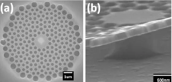
At the wet-etching step, to well control the post formation, the temprature of diluted HCl solution is fixed at 2 °C to slow down the etching rate, estimated to be 1.05 µm / min along <-1,0,0> direction of InP [26]. And we will define the effective post size as two times the distance from microcavity center to the outermost position occupied by the post, which is aimed at fairly estimating the influence on WG mode caused by the post. When we vary the wet-etching time from 110 to 160 seconds with air-hole radius (r) over lattice constant (a) ratio (r/a ratio) fixed on 0.37, we observe the effective post size in diamter (D) varied from 1.4 µm to 500 nm, which is inverse-proportional to the wet-etching time, as shown in Fig. 2. 6 (a). On the other hand, when the wet-etching time is fixed at 130 seconds and the air-hole radius of QPhC is varied from 175 to 210 nm, D is also inverse-proportional to the increase of air-hole radius, as shown in Fig. 2. 6 (b). This is a reasonable relationship due to loading effects of different air-hole sizes during the wet-etching process. The top-view SEM pictures of microcavities with D = 480, 650, and 900 nm are shown in Fig. 2. 6 (c)
Fig. 2. 6 : (a) The plot of the effective post size versus wet-etching time when the r/a rato is 0.37. (b) The plot of the effective post size versus the air-hole radius when the wet-etching time is 130 seconds. (c) Top-view SEM pictures of microcavities with D = 480, 650, and 900 nm.
2.4 Measurement Results
2.4.1 Measurement Setup
The 12-fold QPhC D2 microcavities with post size D ~ 830 nm are optically
pumped at room temperature by an 845 nm diode laser with 25 ns pulse width and 0.5 % duty cycle. And the emitted light is collected through a 50× objective lens ,and fed into multimode fiber then detected by an optical spectrum analyzer, Ando AQ-6315A,
20
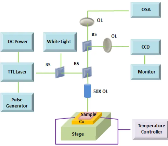
with resolution of 0.05 nm. To investigate the heat sink improvement provided by the post, we will change the Cu-substrate tempetaure with temperature controller, 325B. The illustration of micro-PL measurement system with temperature controlling system is shown in Fig. 2. 7.
Fig. 2. 7 : The illustration of micro-PL measurement system with temperature controlling system.
2.4.2 Lasing Properties
To improve the heat dissipation, the nano-post size should be as large as possible; however, too large post size will disturb cavity mode and induce degradation of Q
factor. Thus, we will focus on the devices with large nano-post size D ~ 830 nm after considering the trade-off between thermal properties improvement and Q factor.
The fabricated lattice constant and r/a ratio are 520 nm and 0.34. We obtain WG6, 1 single-mode lasing at 1485 nm. The lasing spectrum above threshold and measured
light-in light-out (L-L) curve are shown in Fig. 2. 8 (a) and (b). The threshold is estimated to be 0.6 mW from the L-L curve. And the spectral line width is estimated to be 0.18 nm from the spectrum at 0.8 times threshold shown in the inset of Fig. 2. 8 (b) by Lorentzian fitting, which corresponds to a Q factor of 8,250. With large inserted nano-post, above lasing properties are significantly improved compared with those we demonstrated before (Q ~ 6,300 and threshold ~ 1.2 mW from the microcavity with similar nano-post size) [6]. These are attributed to the improvement in our fabrication process, including the air-hole shape and sidewall angle, which both reduce unnecessary optical losses.
Fig. 2. 8 : (a) The measured lasing spectra above and below threshold at wavelength of 1485 nm. The measured spectral line width near threshold is 0.18 nm by Lorentzian fitting. (b) L-L curve of 12-fold QPhC D2 microcavity with nano-post size D of 830
nm. The threshold is estimated to be 0.6 mW and the SEM picture of measured device is also shown in the inset.
22
Besides, we also observe mode-hopping effect. The two single mode lasing wavelengths we observed are 1470 and 1410 nm with D = 700, 1100 nm, respectively, as shown in Fig. 2. 9 (a) and (b), which correspond to WG6, 1 and WG3, 2 modes by
comparing them with our simulated results reported previously [6]. From the statistical measured results, we can find the lasing action at 1470 nm from the high Q WG6, 1 mode when D < 830 nm. However, once the post becomes further larger, the
lasing mode will hop to WG3, 2 at 1410 nm. This is because the WG6, 1 mode is
destroyed by the too large post and WG3, 2 will take the lead in mode competition.
Although the WG3, 2 mode field is more concentrated at the center of microcavity
compared with WG6, 1 mode field, it will be enhanced by the micro-cylinder effect [27]
when the enlarged nano-post size is larger than the mode field concentrated region
Fig. 2. 9 : The lasing spectra of 12-fold QPhC D2 microcavity from (a) WG6, 1 and (b)
WG3, 2 mode at 1470 and 1410 nm, with D = 700, 1100 nm
2.4.3 Measurement with Different Substrate Temperature
To investigate the heat sink improvement provided by the post, we change the substrate tempetaure of microcavity with post D = 830 nm with temperature
controlling system. WG6, 1 single-mode lasing action can still be obtained when the
substrate temperature is as high as 70 °C, which is higher than the temperature limitation of 52 °C from 12-fold QPhC D2 microcavity without nano-post. This
observed lasing action at high substrate temperature of 70 °C is also better than those in PhC membrane microcavities with larger and similar microcavity sizes [25] [28], which can be attributed to the extra heat sink provided by the nano-post beneath. The measured L-L curves of WG6, 1 mode lasing when the substrate temperature is varied
from 20 to 70 °C are shown in Fig. 2. 10 (a). The threshold increases exponetially with the increased substrate temperature, as shown in Fig. 2. 10 (b). This is reasonable because there would be extra injected carrier wasting in non-radiative surface recombination, which leads to the increase of threshold when the substrate temperature increases.
Fig. 2. 10 : (a) L-L curves of microcavity with nano-post size D = 830 nm under substrate temperatures of 20, 35, 50, 60, and 70 °C, respectively. (b) The relationship between the threshold and the substrate temperature.
24
increases from 20 to 70 °C with 2 °C increment. We obtain total lasing wavelength red-shift of 2.5 nm, which corresponds to 0.050 nm / °C red-shift rate by linear fitting, as shown in Fig. 2. 11. For comparison, we obtain the red-shift rate of 0.086 nm / °C from QPhC D2 microcavity without nano-post, which is larger than 0.050 nm / °C of
microcavity with nano-post under the same pump condition. Thus, we can conclude that the nano-post plays the role of heat sink and improves the heat dissipation indeed.
Fig. 2. 11 : The lasing wavelength variation plot when the substrate temperature is varied from 20 to 70 °C. The red-shift rate is about 0.050 nm / °C, which is smaller than that (0.086 nm / °C) of microcavity without nano-post beneath.
2.4.4 Measurement with Different Pump Duty Cycle
From the improved thermal properties obtained in experiments above, we can see the potential of post structure to be operated under CW condition. We then increase the duty cycle of pump source. The measured L-L curves when the pump duty cycle is varied from 0.5 to 16.0 % are shown in Fig. 2.12 (a). When the pump duty cycle is increased to 8.0 %, the threshold increases as shown in Fig. 2. 12 (a) and (b) but there is no significant change in slope efficiency compared with that when the pump duty
cycle is 0.5 %. However, when the pump duty cycle further increases to 16.0 %, the threshold increases to 1.0 mW and the slope efficiency decreases significantly, as shown in Fig. 2. 12 (a). The increase of threshold and decrease of slope efficiency could be both attributed to the similar reasons of the degradations due to the increased substrate temperature.
Fig. 2. 12 : (a) L-L curves of microcavity with nano-post beneath under different pump duty cycles from 0.5 to 16.0 %. (b) The relationships of the pump duty cycle versus the spectral line width and the threshold. Both spectral line width and threshold increase with the increasing pump duty cycle.
26
Besides, we also observe broadened spectral line width with increased pump duty cycle near threshold, as shown in Fig. 2. 13, which directly indicates the increase of microcavity temperature with the increase of pump duty cycle. When the pump duty cycle further increases to 20.0 %, the WG6, 1 mode lasing action is not always
observed and the MQWs are destroyed when the pump duty cycle is larger than 20.0 %. Although the CW operation is not available in this study, it is evident that the nano-post plays an efficient heat sink and improves the thermal performances of 12-fold QPhC D2 microcavity. Thus, we still believe the CW operation can be
obtained by this design with optimizations, for example, MQWs gain peak (near 1550 nm at room temperature) alignment with the microcavity resonance, improvement of fabrication imperfections, and so on.
Fig. 2. 13 : The measured WG6, 1 mode spectra near threshold when the pump duty
cycles are 0.5, 2.0, 4.0, and 8.0 %. The spectral line width is broadened due to the increasing thermal effect from the increased pump duty cycle.
2.5 Conclusion
In this chapter, we introduce the fabrication process of 12-fold QPC D2
microcavity with size-controlled central post by fine-tuning the wet-etching time with appropriate r/a ratio. By FEM simulation, we have simulated the heat transition behaviors of microcavities with different post sizes (0 to 800 nm) and shapes (tilted angle = 90° to 60°). And we can conclude that large post with tilted angle will provide better heat dissipation comparing with membrane structure. In addition, larger post also provides the smaller electrical resistance and it would benefit for electrically-driven. In measurements, from microcavity with nano-post size D = 830 nm, we obtain WG6, 1 mode lasing at 1470 nm with high measured Q factor of 8,250
and low threshold of 0.6 mW, For experimental thermal characterizations, the WG6, 1
mode lasing action from microcavity with nano-post size D = 830 nm is still observed when the substrate temperature is as high as 70 °C. And we obtain the lasing wavelength red-shift rate of 0.050 nm / °C when varying the substrate temperature, which is better than 0.086 nm / °C from microcavity without nano-post beneath. Besides, the WG6, 1 mode lasing action is still observed when the pump duty cycle is
up to 16.0 %. According to these results in simulations and experiments, we believe the realization of electrically-driven PhC microcavity laser under CW operation can be strongly expected based on this post structure.
28
Chapter 3 Realization of
Electrically-Driven Photonic Crystal
Microcavity Laser
3.1 Introduction
In this chapter, we will focus our researches on the fabrication of electrically-driven 12-fold D2 quasi-photonic crystal microcavity. The complicated
fabrication processes can be classified into two parts, mesa structure and photonic crystal patterns. There will be many problems in the processes of forming the mesa structure and defining photonic crystal patterns, and we will discuss about these issues in detail. For comparison, both electrical and optical properties of the post structure without photonic crystal pattern will be measured. And the electro-luminescence and several lasing properties of the electrically-driven QPC microcavity will also be investigated in the final.
3.2 Fabrication Processes
Fig. 3. 1 (a) and (b) show the basic mesa structure and wafer structure of electrically-driven photonic crystal microcavity. For electrically driving, the epitaxial structure is heavily doped ~ 1018/cm3 , which is different from that of membrane structure. The current will be injected from Au electrode on the top of quantum wells and InP under the quantum wells, and recombine at the photonic crystal region.
Because the electron mobility is larger than hole, we then design the n-i-p heterojunction structure to increase the injection efficiency and make the recombination between electrons and holes can concentrate on the microcavity.
30
Fig. 3. 1 : Illustration of the device structure after (a) mesa structure formation process and (b) photonic crystal pattern. (c) The wafer structure of electrically-driven photonic crystal microcavity.
The fabrication processes can be divided into two parts, mesa structure formation and photonic crystal pattern, as shown in Fig. 3. 2 and Fig. 3. 3.
The processes of mesa structure include four steps : (A) First, SiNx deposited by
PECVD. And then define the pattern of mesa by photolithography and transfer it to SiNx and InP layer in sequence by a serious of ICPRIE dry-etching processes. (B) The
sacrificed layer under the MQWs layer will be etched by diluted HCl selective wet-etching process, and the disk structure will be formed with the large post beneath MQWs layer. Due to the disk structure is unstable, the etched undercut will be filled with photon resist (PR) .The PR under the quantum wells can both enhance the mechanical stability and isolate current through non-post region at the same time. (C) Then the remnant PR and SiNx will be removed by O2 plasma and BOE wet-etching.
Before next step, we will hard bake the PR to make it not be dissolved by acetone solution. (D) Finally, we will do the photolithography the second time, and then deposit Au/Ge/Ni electrode by E-gun. After lift-off, the mesa structure with electrode is fabricated.
And the process of photonic crystal pattern include two steps : (E) First, SiNx
deposited by PECVD. And then define the pattern of photonic crystal by E-beam lithography and transfer it to SiNx and InP layer in sequence by a serious of ICPRIE
dry-etching processes. (F) Fabrication of the central nano-post under quantum wells by dilute HCl solution wet-etching process.
32
Fig. 3. 3: The fabrication processes of photonic crystal pattern.
3.2.1 Fabrication Processes of Mesa Structure
3.2.1.1 Photolithography the First Time and ICP Dry-Etching
At first, we will deposit SiNx layer of 140 nm on the InP by PECVD. The SiNx
layer here is served as hard mask for quantum wells beneath it. Then we will define the mesa pattern by photolithography process. Here we design the mesa sizes of 40, 50, and 60 μm in diameter, respectively, which are smaller than that of 70, 90, and 110 μm we used before due to the too large mesa size will easy to collapse, and we can shrink the device size at the same time. The mesa mask pattern is shown in Fig. 3.
4. The electrode is designed in ring-shape with the width of 10 μm, and have margin of 2 μm with the mesa edge to keep a tolerance in the second time photolithography. The distance between mesas is 100 μm, and the rectangle and cross shape are alignment keys to help us align in photolithography steps.
The PR that we used is FH-6400. The parameters of PR spinning are 1,000 and 4,000 rev / sec for 10 and 30 second, respectively. The thickness of the PR in this recipe is about 1.6 µm. This thick PR layer will not be removed before the following undercut step, because it can prevent the MQWs collapse from the van der Waals force. The exposure and develop time in this recipe are 30 and 60 seconds, respectively. The developing dilute is FHD-5. Subsequently, we will etch the SiN and InP by a serious of ICP-RIE dry-etchig processes. We will transfer the patterns of mesas to SiN without cleaning PR. And then transferring patterns to QW and InP. The etching of InP recipe should be as short as possible or it will destroy the PR layer on the top. Now, the mesa without undercut has been fabricated.
34
Fig. 3. 4: Photo mask design of mesa (40、50、60 µm in diameter) and electrode (10µm).
3.2.1.2 Undercut the First Time and PR Filling
After the mesa is formed, we then fabricate the undercut under MQWs by
wet-etching process without remnant PR removing. The undercut is aim to produce the large post, which is the region we will write photonic crystal pattern on and prepared for current pathway fabrication. And we don’t remove the remnant PR from the first time photolithography for holding the MQWs, and prevent it bending from ven der Waals force. At the wet-etching step, the dilute HCl solution of HCl : H2O =
3 : 1 at room temperature is used for large etched region, the wet-etching rate and time are 10 μm and 67 second, respectively. The parameter of wet-etching time is crucial for the characteristics of device, which affect the size of the large post; too large post size will induce large leaky current and force the electrical property bad, as shown in Fig. 3. 5 (a) and (b) , however, too small post size will lead to MQWs slab bend and destroy the structure of quantum wells, as shown in Fig. 3. 5 (c) and (d) . Besides, the height of post is 800 nm as the same as p-InP sacrificial layer, and the height of filled PR would also be 800 nm without the MQWs slab bending. After numerous experiments, we then find the wet-etching time of 65 second with 40 μ m-diameter-mesa at room temperature will be appropriate for post fabrication.
36
Fig. 3. 5 The tilted and cross-section SEM picture of the (a) (b) too large post size and (c) (d) too small post size. The remnant PR on the top of these SEM pictures have been cleaned in the following step.
After the undercut fabrication, we should fill it with PR instantly, otherwise, the MQWs layer will easy to bend for freestanding. The filled PR here not only to hold MQWs layer, but be a current block to isolate the MQWs and substrate, forcing injected current drift through the region of photonic crystal pattern. And we achieve the PR filling by spin coater with rotation of 1,000 and 4,000 rev / sec for 10 and 5 second, respectively. The tilted and cross-section SEM picture of the sample filled with PR successfully with appropriate size is shown in Fig. 3. 6 (a) and (b).
Fig. 3. 6: The (a) tilted and (b) cross-section SEM picture of the sample filled with PR under MQWs slab successfully with appropriate post size. And the remnant PR on the top of these SEM pictures have been cleaned in the following step.
We have fabricated the large post in two cases of 40 and 50 μm in diameter. For mesa of 50 μm in diameter, the large post is fabricated with wet-etching time of 85 and 90 second, as shown in Fig. 3. 7. The post size and height of filled PR are about 33.3 μm and 450 nm with wet-etching time of 85 second, as shown in Fig. 3.7 (a) (b), and those are about 28 μm and 334 nm with wet-etching time of 90 second, as shown in Fig. 3.7 (c) (d). Due to the freestanding region of MQWs layer is seriously bending and the MQWs are destroyed, we then try to fabricate the large post with mesa of 40μm in diameter.
38
Fig. 3. 7: The tilted and cross-section SEM picture of 50μm-diameter-mesa filled with PR under MQWs slab ,and the post size and height of PR are 33.3 μm and 450 nm for wet-etching time of 85 second (a) (b) , 28 μm and 334 nm for wet-etching time of 90 second (c) (d). And the remnant PR on the top of these SEM pictures have been cleaned in the following step.
For mesa of 40 μm in diameter, the large post is fabricated with wet-etching time of 60, 65, and 70 second, as shown in Fig. 3. 8. The post size and height of filled PR are about 24.6 μm and 771 nm with wet-etching time of 60 second, as shown in Fig. 3.8 (a) (b), and those are about 21.6 μm and 750 nm with wet-etching time of 65 second, as shown in Fig. 3.8 (c) (d), 17.1 μm and 253 nm with wet-etching time of 70 second, as shown in Fig. 3.8 (e) (f). The wet-etching time of 60 second can successfully fill the PR in the wet-etched region and not induce slab bending, but the post size is a little bit large for the case of 40μm-diameter-mesa. On the other hand, the wet-etching time of 70 second could fabricate a small post size to prevent the leaky current through, however, the MQWs layer bending is still serious, such as in 50
μm-diameter-mesa case. Consequently, we will choose the wet-etching time of 65 second due to the acceptable post size and undestroyed MQWs layer in 40μ m-diameter-mesa case.
Fig. 3. 8: The tilted and cross-section SEM picture of 40μm-diameter-mesa filled with PR under MQWs slab ,and the post size and height of PR are 24.6 μm and 771 nm for wet-etching time of 60 second (a) (b) , 21.6 μm and 750 nm for wet-etching time of 65 second (c) (d), 17.1 μm and 253 nm for wet-etching time of 70 second (e) (f). And the remnant PR on the top of these SEM pictures have been cleaned in the following step.
40
3.2.1.3 Remnant PR Clean, and Hard Bake
For the following lithography and electrode deposited steps, we need to clean the remnant PR and SiNx on the top of MQWs slab. First, we use O2 plasma to
remove the most remnant PR, and then the less remnant PR will be cleaned clearly after removing SiNx by BOE wet-etching process. In Fig. 3. 9 (a) , we apply O2
plasma of 2 min, and the mesa is still with few remnant PR. In Fig. 3. 9 (b), the remnant PR is removed completely with O2 plasma for 3 min, and we can see the post
shape exactly in the top view. The SEM pictures from Fig. 3. 5 to Fig. 3. 8 are all processed with remnant PR and SiNx removing.
Considering the filled PR may be dissolved by acetone at the lift-off step, we will hard bake the sample at high temperature of 300 ℃ for 2 min by hot plate before the second time lithography. And the filled PR will be harden that undissolvable by acetone.
Fig. 3. 9 : The tilted SEM picture with O2 plasma of (a) 2 min and (b) 3 min. The
3.2.1.4 Photolithography the Second Time and Electrode Deposited
Then we will define the pattern of electrode by the second photolithography. Although the pattern may not in the center of mesa correctly due to the alignment is not east to perform, we can still compensate it by aligning at E-beam lithography step. And we will deposit the electrode of Au/Ge/Ni for 200/35/35 nm by E-gun evaporator. The electrode is designed for ring-shape for effectively current injected. After lift-off, the mesa structure with ring-shape metal contact is successfully fabricated, as shown in Fig. 3. 10 (a) (b) .
Fig. 3. 10 : (a) (b) The SEM pictures of mesa structure successfully fabricated with ring-shape Au/Ge/Ni metal contact.
After fabrication process of mesa structure, we measure the I-V curve by HP-4156B. The measured result of 40μm-diameter-mesa structure is shown in Fig. 3. 11 (a). We also fabricate 50μm-diameter-mesa structure without PR filling for comparison in following step, the measured I-V curve is shown in Fig 3. 11 (b). We can know the mesa structure that is a p-n diode from Fig. 3. 11 and we can also
42
confirm that the Au/Ge/Ni electrode is ohmic contact. The turn-on voltage and resistance of 40μm-diameter-mesa are about 4.51 V and 523 Ω, and that of 3.88 V and 550.9 Ω for 50μm-diameter-mesa.
Furthermore, we also measure the PL (photoluminescence) spectrum of original sample (unprocessed), 40 and 50μm-diameter-mesa structure, as shown in Fig. 3. 12, the intensity of emission peak are 826.4, 672.2, and 569 pW, respectively, with pump power of 1.7 mW. And we find the MQWs layer is degraded for a little.
Fig. 3. 11 : The measured I-V curve of device (a) with PR and (b) without PR, the turn-on voltage of each are 4.51 V and 3.88 V, and the resistance of each are 523 Ω and 550.9 Ω, respectively.
Fig. 3. 12 : The measured PL spectra of (a) original sample (unprocessed), (b) mesa with PR and (c) without PR, with intensity of emission peak of 826.4, 672.2, and 569 pW, respectively, with pump power of 1.7 mW.
3.2.2 Fabrication Processes of Photonic Crystal Pattern
3.2.2.1 Define Pattern by E-beam Lithography
Now, the mesa structure with large post and filled PR beneath MQWs layer and metal contact deposited on the top have been fabricated. And we will define the pattern of 12-fold quasi-photonic crystal microcavity by E-beam lithography in this step. The inaccuracy between 1st and 2nd mask of photolithography will make metal contact apart from mesa center, to compensate it, we use alignment function of E-beam to define photonic crystal pattern in the center of mesa and on the top of large post. By applying the alignment function, photonic crystal pattern can be written on the mesa more accuracy then we didn’t use before.
3.2.2.2 ICP Dry-Etching
After writing photonic crystal pattern on the PMMA, we then use a series of dry etch by ICPRIE to transfer the pattern into SiNx mask InGaAsP MQWs and InP
substrate. The gas we used to etch SiNx and InP are CHF3/O2 and CH4/H2/Cl2 ,
respectively. In Fig. 3. 13 , we show the SEM pictures of device with photonic crystal pattern drawn on. Part of the pattern is not right on the top of the large post due to inaccuracy of alignment in photolithography and E-beam lithography, but if we can fabricate the nano-post beneath MQWs layer, the device can still be driven by inject current.
44
Fig. 3. 13 : Top view SEM pictures of mesa with PR after pattern defining and dry-etching (left) and the 12-fold D2 quasi-photonic crystal pattern (right).
We also fabricate device without undercut and PR filling before pattern defining to compare electrical and lasing properties with the PR-filled-structure, as shown in Fig. 14. The pattern is written on the 50μm-diameter-mesa, and the air holes out of 12-fold quasi-photonic crystal pattern are set to decrease the volume of InP, the pathway leaky current.
Fig. 3. 14 : Top view SEM pictures of device without undercut after pattern defining and dry-etching (left) and the 12-fold D2 quasi-photonic crystal pattern (right).
3.2.2.3 Undercut Second Time
The last step of all fabrications is undercut again to fabricate the nano-post beneath MQWs layer to be the current pathway for electrically-driven. In section 2 . 3, we have investigated the relationship between wet-etching time and r / a ratio. Take it into consideration, we fabricate the nano-post by HCl : H2O = 3 : 1 selective
wet-etching process for 140 second at 2 °C to slow down the etching rate. And we will define the effective post size as two times the distance from microcavity center to the outermost position occupied by the post, which is aimed at fairly estimating the influence on WG mode caused by the post. After wet-etching process, the nano-post with effective post size of 776 nm is fabricated, which satisfies the post size condition (< 830 nm) for WG6.1 mode, besides, the r / a ratio and lattice constant equal to 0.40
and 520 nm, as shown in Fig. 3. 15 (a) (b) (c). In addition, from Fig 3. 15 (d), the tilted 45° SEM picture, we can see bottom of nano-post from the air hole nearest to the cavity.
46
Fig 3. 15 : (a) The top-view SEM picture of the complete device of electrically-driven photonic crystal microcavity. (b) 12-fold D2 quasi-photonic crystal microcavity
pattern with central nano-post. (c) The effective post size is estimated to be 776 nm, satisfying the post size condition (< 830 nm) for WG6.1 mode. (d) The tilted 45° SEM
picture of cavity, the bottom of nano-post is observed from air hole nearest to cavity.
The SEM of device without PR is shown in Fig. 13. The effective post size is estimated to be 666 nm ,which satisfies the post size condition (< 830 nm) for WG6.1
mode, besides, the r / a ratio and lattice constant equal to 0.39 and 520 nm, as shown in Fig. 3. 16 (a) (b) (c). Additionally, the post is observe clearly from the tilted 45° SEM picture of large nano-post, the effective post size and r / a ratio is about 1340 nm and 0.36, as shown in Fig. 3. 16 (d) (e) (f).
![Fig. 1. 4: The PBG gap map of square and triangular lattice photonic crystal. ( Adopted from reference [8] )](https://thumb-ap.123doks.com/thumbv2/9libinfo/8390048.178668/16.892.162.736.566.799/fig-square-triangular-lattice-photonic-crystal-adopted-reference.webp)