國 立 交 通 大 學
光 電 工 程 研 究 所
碩 士 論 文
利用珈瑪氧化鋁為緩衝層成長於(111)矽晶圓的
氧化鋅磊晶薄膜之結構與光性研究
Structural and optical properties of ZnO
epi-layer grown on Si(111) using a γ-Al
2O
3buffer layer
研 究 生:李 岳 勳
指 導 教 授:徐 嘉 鴻 教授
謝 文 峰 教授
中 華 民 國 九 十 七 年 六 月
利用珈瑪氧化鋁為緩衝層成長於(111)矽晶圓的
氧化鋅磊晶薄膜之結構與光性研究
Structural and optical properties of ZnO
epi-layer grown on Si(111) using a γ-Al
2O
3buffer layer
研 究 生:李岳勳 Student: Yueh-Hsun Li
指導教授 :徐嘉鴻 教授 Advisor: Dr. Chia-Hung Hsu
謝文峰 教授 Dr. Wen-Feng Hsieh
國立交通大學
光電工程研究所
碩士論文
A Thesis
Submitted to Institute of Electro-Optical Engineering College of Electrical Engineering and Computer Engineering
National Chiao Tung University in Partial Fulfillment of the Requirements
for the Degree of Master
in
Electro-Optical Engineering June 2008
Hsinchu, Taiwan, Republic of China
利用珈瑪氧化鋁為緩衝層成長於(111)矽晶圓的氧化鋅磊晶薄
膜之結構與光性研究
研究生: 李岳勳 指導教授: 徐嘉鴻教授 謝文峰教授 國立交通大學電機學院光電工程研究所 摘要 藉由一層珈瑪氧化鋁緩衝層將高品質氧化鋅薄膜以雷射濺鍍方法磊晶成長於 (111)面的矽晶圓上,此珈瑪氧化鋁緩衝層含有以晶面(111)為軸向的兩種彼此旋 轉 60 度的結構空間分布。樣品在垂直表面方向的磊晶結構關係為氧化鋅(0002)// 珈瑪氧化鋁{22-4}或{4-2-2}//矽晶圓{22-4}。利用X光繞射、穿透式電子顯微鏡 與螢光光譜來量測氧化鋅的晶體結構與光學特性,我們發現深層能階發光的強度 相對於能隙發光強度比與薄膜的φ角半高寬大小有明顯的關聯;而能隙發光光譜的 半高波寬分布大小與薄膜的表面晶面方向分布有關。這個關聯也就代表螺旋型差 排缺陷主要與能隙發光光譜有關,而邊刃型差排缺陷主要與深層能階發光有關。Structural and optical properties of ZnO epi-layer grown on
Si(111) using a γ-Al
2O
3buffer layer
Student: Yueh-Hsun Li Advisors: Prof. Chia-Hung Hsu Prof. Wen-Feng Hsieh
Institute of Electro-Optical Engineering National Chiao Tung University
Abstract
High-quality ZnO epitaxial films were grown by pulsed-laser deposition on Si(111) substrates with a thin γ-Al2O3 buffer layer. The epitaxial γ-Al2O3 buffer layer consists
of two (111) oriented domains rotated 60o from each other against the surface normal.
Therefore, two in-plane epitaxial relationships {1010}_ ZnO||
2 3 -Al O {224}γ || {224}Si and || || _ ZnO {1010} 2 3 _ _ -Al O
{4 2 2}γ {224}Si coexist. The crystalline quality and optical properties of ZnO epi-layers were studied by x-ray diffraction, transmission electron microscopy and photoluminescence measurements. A clear correlation between the intensity ratio of ZnO deep-level emission (DLE) to near-band edge (NBE) emission and the width of the φ-scan across off-normal reflection was observed. The NBE linewidth also exhibits a strong dependence on the width of the ZnO (0002) rocking curve. These observations indicate the NBE and the DLE emissions are mainly affected by the screw and the edge type threading dislocations, respectively.
誌謝 時間過得真快,兩年就這樣過去了,回想這七百多個日子裡真是嘗盡了心酸也 充滿了歡笑,也在這點點滴滴的過程中學到了不少;首先要非常感謝我的指導教授 徐嘉鴻老師以及教授謝文峰老師的指導,在老師們的指導下讓我在知識上獲益良 多,還有維仁學長的指教和領導,同時也很感謝由洪銘輝教授以及郭瑞年教授所帶 領的清華大學材料所先進奈米磊晶實驗室所提供的試片,以及實驗室和同步輻射 研究中心的所有學長姐學弟妹同儕們的幫忙,讓我可以很充實很順利地度過這兩 年 的 時 光 , 同 時 也 感 謝 國 科 會 計 畫 ( 計 畫 編 號 : NSC-96-2119-M-213-003 和 NSC-96-2628-M-009-001-MY3) 的贊助,讓我可以專心於實驗。 最後要感謝我的父母親友們,謝謝你們這些年來源源不絕給我的支持和愛護, 讓我在學業以及生活上獲益良多。
Content
Chinese Abstract………i
English Abstract………ii
Acknowledgement………iii
Contents……….iv
List of Figures………..vii
List of Tables……….ix
Chapter 1 Introduction
……….………..-1-1-1 A brief review
1-2
Motivation
……….-2-1-3 Organization of the thesis
……….…-4-Chapter 2 Theoretical background
……….-5-2-1 The laser-MBE system and principle of laser-MBE
Deposition
……….-5-2-2 X-ray diffraction
……….-8-2-2-1 Theory of x-ray diffraction………...………….-8-
2-2-2 Rocking curve………-11-
2-3 Transmission electron microscopy
…………...……….…-16-2-3-1 Selected area electron diffraction (SAED)…..……….-17-
2-3-2 Analysis of threading dislocation density….….………...-18-
2-4 Photoluminescence characterization
2-4-1 Fundamental Transitions………-23-
Chapter 3 Experimental details
………-26-3-1 The growth of ZnO films
………..-26-3-1-1 Description of laser-MBE system……….-26-
3-1-2 The layout of laser-MBE system………..…-27-
3-1-3 Target preparation………....-28-
3-1-4 Preparation of substrate………...-28-
3-1-5 Operating process of laser-MBE………..-29-
3-2 Structural characterization of the ZnO films
………..….-31-3-2-1 X-ray diffraction………....-31-
3-2-2 Cross sectional TEM……….………-32-
3-3 Measurements of optical properties
……… .………...-33-3-3-1 Photoluminescence detection system………..………..-33-
Chapter 4 Results and Discussion
4-1-2 Analysis of threading dislocation density by XRD………..-41-
4-2 Structural characterization by TEM
………….………46-4-2-1 Cross sectional TEM………..-46-
4-2-2 Analysis of threading dislocation density………...……..-48-
4-3 Optical characterization by PL
……….….-51-4-3-1 photoluminescence spectra of as-grown film………...-51-
4-4 Correlation between structural and optical properties
of ZnO films
………..………..-55-Chapter 5 Conclusions and Perspective
……….…-59-5-1 Conclusions
5-2
Perspective
………....-59-………-68-List of Figures
Fig. 1-1 Wurtzite structure………..…2
Fig. 2-1 Schematic of a laser-MBE growth system………....7
Fig. 2-2 X-ray scattering from a cubic crystal……….10
Fig. 2-3 The hexagonal unit cell……….………...10
Fig. 2-4 Illustration of phi scan……….11
Fig. 2-5 Illustration of Burgers vector and types of dislocations………...16
Fig. 2-6 The TEM image contrast of a wedge-shaped specimen………21
Fig. 2-7 Radiative transitions between a band and an impurity state…………...25
Fig. 3-1 Layout of laser-MBE system………...27
Fig. 3-2 The preparation process of a cross-sectional TEM specimen…………..33
Fig. 3-3 Layout of PL system………..………...34
Fig. 4-1 Radial scan along the surface normal of a sample……….…...37
Fig. 4-2 The profile of φ–scans across ZnO {10-10}, γ-Al2O3(440) and Si{220} reflections……….37
Fig. 4-3 Correlation between growth temperature and ZnO structural quality..40
Fig. 4-4 Williamson-Hall plots of ZnO layers………..44
Fig. 4-5 Williamson-Hall plots for transverse scans………45
Fig. 4-8 Typically PL spectra measured at 15K for ZnO epi-layers……….…….53 Fig. 4-9 The extended spectra of NBE emission of ZnO film……….54 Fig. 4-10 Dependence of PL FXA peak intensity on sample temperature....……..54
Fig. 4-11 Correlation between structural and optical properties………...57 Fig. 4-12 Correlation between threading dislocation densities and optical
properties………...……….58 Fig. 5-1 PL spectra of ZnO film before and after annealing ……….64 Fig. 5-2 PL spectra of thickness dependent ZnO films before and after
annealing……….….65 Fig. 5-3 Structural properties of thickness dependent ZnO film.……….…66 Fig. 5-4 X-ray reflectivity curves of samples before and after annealing……….67
List of tables
Chapter 1 Introduction
1-1 A brief review
Zinc oxide is a crystal of hexagonal wurtzite structure with the lattice constants of a = 3.24 Å and c = 5.20 Å as shown in Fig. 1-1. ZnO has been considered as one of the most promising candidates for the materials used in short-wavelength photonic devices because of its wide band gap of 3.37 eV and large exciton binding energy of 60 meV at room temperature [1]. In contrast to technical limitations of GaN (band gap = 3.4eV), exciton of ZnO is stable even at elevated temperature. Recently, the strong commercial desire for blue and ultraviolet diode lasers and light emitting diodes has prompted enormous research efforts into II-VI wide band gap semiconductors [2]. In 1997, Y. F. Chen, et al. [3] demonstrated the lasing from ZnO epilayers grown by MBE with the threshold intensity of 240 KW/cm2. In 1998, Kawasaki et al. [4], found laser operation of ZnO thin film at room temperature grown using laser-molecular beam epitaxy. The lasing mechanism is attributed to the exciton-exciton collision process. In order to obtain good quality of ZnO thin film, several growth technologies have been used such as molecular-beam exptaxy (MBE) [5], metal-organic chemical vapor deposition (MOCVD) [6], and laser molecular-beam epitaxy (LMBE) [7]. Among these methods, LMBE has the advantages of ultra-clean, simplicity, without corrosive
gas, (220 Besid oxyg oxyg oxida and achiev oC~500 oC
des, the sou gen supply gen atmosph ation of the ving high-qu C) due to its urce of Zn is necessar here during internal pa uality epitax high kineti and O can ry. This p g the laser arts in the ch xial films a ic energy (1 be obtained process is i ablation le hamber. at a relative 0 eV~100 e d directly fr important f eads to sev
ely low gro eV) of laser from the tar for some de eral proble owth temper r ablated spe rget, i.e. no evices sinc ems, such a rature ecies. extra ce the as the
1-2
Re subst withMotivat
ecently, mu trates becau ZnO-basedtion
uch attentio use of the un d optoelectro Fig. 1-on has bee nique possib onic device -1 Wurtzite en paid to bility of inte es. Unfortu e structure heteroepita egrating we unately, dire axially gro ell-establish ect growth own ZnO o hed Si electr of epitaxial on Si ronics l ZnOfilms on Si is an extremely difficult task due to the formation of an amorphous SiO2
layer at the ZnO/Si interface [8, 9] that usually results in polycrystalline films with preferred orientation [10]. Although significant efforts have been made to use nonoxide materials, such as ZnS [8], Si3N4 [9], Zn/MgO [11] and Mg/MgO [12], as
buffer layers, the growth of high-quality ZnO epi-films on Si is still regarded as an arduous challenge.
The other issue for the growth of high-quality ZnO epi-films is the existence of high-density threading dislocations (TDs) originating from the large difference in the lattice mismatch (−15.4%) and the thermal expansion coefficient (56%) between ZnO (thermal expansion coefficient α 5 × 10⁻⁶ K−1 [13], lattice parameters a = 3.24 Å, c = 5.20 Å) and the underneath Si substrate (α = 3.6 × 10⁻⁶ K−1 [14], a = 5.431 Å). The point defects captured by TDs stress field act as traps and recombination sites forming deep electronic states inside the band gap [15, 16]. They can lead to electron scattering [17], significantly affect the optical performance and electron mobility [16, 18] and adversely demote the device efficiency. In this thesis, we report the growth of high-quality epitaxial ZnO films using pulsed-laser deposition (PLD) on Si (111) substrates with a 15.3 nm thick γ-Al2O3 film as the buffer layer. The good crystal
structure of thin ZnO films was confirmed by x-ray diffraction (XRD) and transmission electron microscopy (TEM). Their optical characteristics were studied using
photoluminescence (PL) and correlated with the structural properties.
1-3 Organization of the thesis
The thesis consists of five chapters. In Chapter 2, we review the background mechanism of Laser-MBE as well as the basic theory of the characterization tools employed semiconductor such as X-ray diffraction, transmission electron microscopy and photoluminescence spectroscopy. In Chapter 3, we describe the experiment details, including the equipment setups, parameter characterization and substrate preparation. In Chapter 4, we present the analysis of ZnO films and establish the correlation between structural and optical properties. In the final chapter, we conclude our investigation and propose the further study on this system.
Chapter 2 Theoretical background
2-1 The laser-MBE system and principle of laser-MBE
deposition
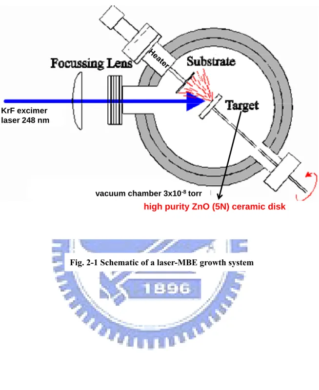
Figure 2-1 illustrates the schematic of a laser-MBE deposition system. Laser beam is shined on the target material. The high heating power leads to the evaporation of the target material, forming a high-temperature plasma plume that expands away from the target surface. The ablated target material is deposited on a substrate and forms a thin film. Depending on the types of interaction of the laser beam with target, the laser deposition process can be classified into three parts:
i. Interaction of laser beam with the target
Upon being struck by a high power density nanosecond excimer-laser pulse, heating and vaporizing the material will occur at the beginning of the pulse. The amount of evaporated flux varies linearly with the pulse energy.
ii. Interaction of the laser beam with the evaporated material
As the evaporated material is heated by the laser beam, it results in the formation of high-temperature plasma plume consisting of ions, atoms, molecules, electrons, etc. The temperature attained by the plasma depends on the power density, frequency, pulse duration of the laser beam, and the optical and thermo physical properties of the
material. During the incidence of the laser pulse, the isothermal expanding plasma is constantly increased at its inner surface with evaporated particle from the target. The acceleration and expansion velocities in this regime are found to depend on the initial velocities of the plasma. The plasma expands preferentially normal to the irradiated surface due to the large lateral dimensions of the plasma.
iii. Adiabatic plasma expansion and deposition of thin films
After the termination of the laser pulse, the plasma expands adiabatically with the expansion velocities controlled by its initial dimensions. The plasma cools rapidly during the expansion process, with the edge velocities reaching asymptotic values. The particles from the expanding plasma strike the substrate and form a thin film with characteristic spatial thickness.
KrF
Focusing lence
KrF excimer laser 248 nm
high purity ZnO (5N) ceramic disk
vacuum chamber 3x10⁻⁸torr
2-2 X-ray diffraction
X-ray scattering techniques are a family of non-destructive analytical techniques which reveal information about the crystallographic structure, chemical composition, and physical properties of materials and thin films. These techniques are based on observing the scattered intensity of an x-ray beam hitting a sample as a function of incident and scattered angle, polarization, and wavelength or energy.
2-2-1 Theory of x-ray diffraction
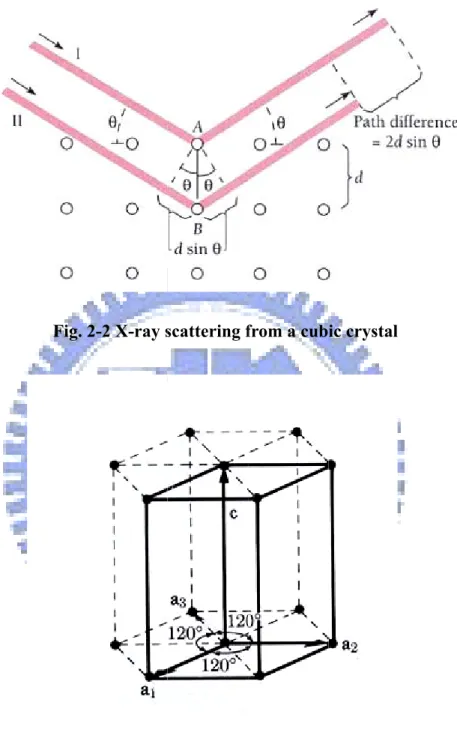
X-ray diffraction finds the geometry or shape of a molecular. X-ray diffraction techniques are based on the elastic scattering of x-rays from structures that have long range order. A crystal consists of a regular array of atoms, each of which can scatter electromagnetic waves. A monochromatic beam of X-ray that falls on a crystal will be scattered in all directions, in certain direction the scattered waves will constructively interfere with one another while others will destructively interfere. The analysis was developed in 1913 by W. L. Bragg. The condition which must be fulfilled for radiation scattered by crystal atoms to undergo constructive interference can be obtained from a diagram like that in Fig. 2-2. In the plane wave description, a beam containing X-rays of wavelength λ impinges on a crystal at an angle θ with a family of Bragg planes, whose space is d. The beam goes past atom A in the first plane and atom B in the next, and each of them scatters part of the beam in random directions. Constructive
interference occurs only between those scattered rays whose paths differ by exactly λ, 2λ, 3λ, and so on. That is, the path difference must be nλ, where n is an integer. The only rays scattered by A and B for which this is true are those labeled I and II in Fig. 2-2. The first condition on I and II is that their common scattering angle is equal to the angle of incidence θ of the original beam. The second condition is that
2dsinθ = nλ, n = 1,2,3,…, (2-1) since ray II must travel the distance 2dsinθ farther than ray I. The integer n is the order of the scattered beam. Then considering a hexagonal unit cell as shown in Fig. 2-3 which is characterized by lattice parameters a and c. The interplanar spacing d for the hexagonal structure is given as:
.
(2-2) Combining Bragg’s law with (2-2):.
(2-3) Rearranging (2-3) g ves i.
(2-4) The lattice parameter a or c can be determined by simultaneously fitting the diffraction angles of different reflections using Eq. 2-4.Fig. 2-2 X-ray sscattering ffrom a cubic crystal
2-2-22 Rocking ccurve calle fixed The the i succe Under a B d rocked th d detector. width of a irradiated a essively com Bragg reflec hrough the B The result rocking cur area of the mes into ref
ction condit Bragg angle tant curve rve is a dire crystal bec flecting pos tion, as sho e θ, while t of intensity ect measure cause each ition as the own in Fig the diffracte y vs. θ is c e of the ran subgrain o crystal is ro g. 2-2, crys ed beam is alled a rock nge of orien of a typica otated [19]. stal is rotat measured w king curve ntation prese l mosaic cr ed or with a [19]. ent in rystal 2-2-33 Phi scan Ph rotati distri hi scan me ing the cry ibution in-p eans to mea ystal along plane polar a asure the d the surface angle φ scan Fig. 2-4 diffraction e normal, a n can reveal intensity v as shown i l the symme vs. azimutha in Fig. 2-4 etry of the c al angle φ . The inte crystal. with ensity
2-2-4 Analysis of threading dislocation density
Figure 2-5 depicts different types of dislocations and the corresponding Burgers vectors. Before characterizing the threading dislocations (TDs), the Burgers vectors should be defined. The Burgers vector, denoted by b, is a vector that represents the magnitude and direction of the lattice distortion of dislocation in a crystal lattice [20]. The magnitude and direction of vector is best understood when the dislocation-bearing crystal structure is first visualized without the dislocation, that is, the perfect crystal structure. In this perfect crystal structure, a rectangle whose lengths and widths are integer multiples of "a" (the unit cell length) is drawn encompassing the site of the original dislocation's origin. Once this encompassing rectangle is drawn, the dislocation can be introduced. Said rectangle could have one of its sides disjoined from the perpendicular side, severing the connection of the length and width line segments of the rectangle at one of the rectangle's corners, and displacing each line segment from each other. What was once a rectangle before the dislocation was introduced is now an open geometric figure, whose opening defines the direction and magnitude of the Burgers vector. Specifically, the breadth of the opening defines the magnitude of the Burgers vector, and, when a set of fixed coordinates is introduced, an angle between the termini of the dislocated rectangle's length line segment and width line segment may be specified. The direction of the vector depends on the plane of
dislocation, which is usually on the closest-packed plane of unit cell. The magnitude is usually represented by equation:
| | √ , for a cubic system, (2-5) where a is the unit cell length of the crystal, |b| is the magnitude of Burgers vector and h, k, and l are the components of Burgers vector, b = <h k l>.
TDs in a film produce crystalline plane distortions and the associated lattice deformation depends on the geometry of the TDs [21]. For a (0001) oriented thin film with wurtzite structure, the TDs are classified into three different types according to the direction of the corresponding Burgers vector (b) relative to the [0001] line direction. They are edge dislocation with bE = 1/3⋅<1120>, screw dislocation with bC = <0001>,
and mixed dislocation with bM = 1/3⋅<1123>, which is a combination of bE and bC.
For edge dislocation, the Burgers vector and dislocation line are at right angles to one another. For screw dislocation, they are parallel. Pure edge TDs twist surrounding hexagonal lattice about [0001], leading to the formation of vertical grain boundaries [22]. Under this circumstance, the (hkil) crystalline planes with nonzero in-plane component, i.e. either h or k is not zero, are distorted. On the other hand, the pure screw TDs result in the tilting of the lattice, generating a pure shear strain field [23], and the crystalline planes with nonzero l are deformed. Therefore, to investigate the influence of edge TDs, measuring the profiles of ( 0 0)h h surface reflections is
necessary, which are not sensitive to lattice distortion caused by pure screw TDs. On the other hand, measuring the line widths of the (000l) normal reflections, which are not affected by the pure edge TDs is a good method to characterize the screw TDs.
The broadening of radial scan line width would come from crystallite size, strain and instrument effects. The experimentally measured FWHM, Bexp, is a convolution of the
instrumental broadening, Binstr., and the broadening coming from the sample, of which
strain induced broadening, Bstrain, and finite crystal size induced broadening , Bsize, are
the major contributions.
As compared with the measured line width of ZnO, the instrumentation induced broadening is much smaller and thus can be safely neglected in our results. To obtain meaningful quantitative results, Williamson-Hall plot [24] is employed to analyze the quantity of domain size and strain. We make a Δqr vs. q plot with q = 4πsinθ/λ
denoting the scattering vector and Δqr standing for the line width in q along the radial
direction to separate the broadening due to finite structural coherence length from strain induced broadening. The equation of the line in Williamson-Hall plot can be expressed as:
∆ ∆ ∆ , (2-6) where L and ε represent the coherent length and inhomogeneous strain, respectively. Thus, the inverse of ordinate intercept yields the coherence length (L), i.e., the effective
domain size, and the slope yields the root-mean-square (RMS) inhomogeneous strain (ε) averaged over the effective domains [24]. The Δqt vs. q plot, where Δqt = Δθ × q
denoting the line width in q along the transverse direction, for θ-scans across the (000l) and in-plane (h0h0) reflections, of which the slopes yield the spreads of tilt and twist angles, respectively. The density of TDs can be evaluated from the corresponding Burgers vectors and the tilt/twist angles. For screw TDs, the density NS is calculated
according to 2 2 4.35 S C N b αΩ
= [25], in which αΩ is the tilt angle and bC denotes the length
of corresponding Burgers vector. For edge TDs, the formula employed to calculate the density, NE, depends on the spatial arrangement of the TDs [26]. Assuming a random
distribution, we can apply
2 2 4.35 αΦ = E E N
b , in which αΦ stands for the twist angle. In the case of TDs accumulating at a small-angle boundary, we should adopt the formula:
2.1 αΦ = E E N
b L, where L denotes the correlation length along the in-plane direction. In both formulae of NE, bE is the length of associated Burgers vector bE = 1/3< 1120 >.
Fig. 2-5 Illustration of Burgers circuits, Burgers vectors, types of edge and screw dislocations
2-3 Transmission electron microscopy
The transmission electron microscope (TEM) has become the premier tool for the micro-structural characterization of materials. In practice, the diffraction patterns measured by x-ray methods are more quantitative than electron diffraction patterns, but electrons have an important advantage over x-ray- electrons can be focused easily [27]. The optics of electron microscopes can be used to make images of the electron intensity emerging from the sample. Several different techniques of TEM often employed for
2-3-1 Selected area electron diffraction (SAED)
SAED is a crystallographic experimental technique that can be performed inside a TEM. A thin crystalline specimen is subjected to a parallel beam of high-energy electrons. The specimens are typically ~100 nm thick, and the electrons typically possess energy of 100 - 400 keV. Thus, electrons can pass through the sample easily. Electrons can be treated as wave-like, rather than particle-like. Because the wavelength of high-energy electrons is a fraction of a nanometer, and the spacing between atoms in a solid is only slightly larger, the atoms act as a diffraction grating to the electrons, which are diffracted. That is, some fraction of them will be scattered to particular angles, determined by the crystal structure of the sample, while others continue to pass through the sample without deflection. As a result, the image on the screen of the TEM will be a series of spots – the selected area diffraction pattern, SADP, each spot corresponding to a satisfied diffraction condition of the sample's crystal structure. If the sample is moved under the beam, bringing different sections of it under illumination, the arrangement of the spots in the diffraction pattern will change. It is useful to select a single crystal for analysis at a time. It may also be useful to select two crystals at a time, in order to examine the crystallographic orientation between them. As a diffraction technique, SADP can be used to identify crystal structures and examine crystal defects. It is similar to x-ray diffraction, but what is unique in that is area as
small as several hundred nanometers in size can be examined, whereas x-ray diffraction typically sample area several centimeters in size.
2-3-2 Analysis of threading dislocation density
The dislocation density D can be obtained by the following equation:
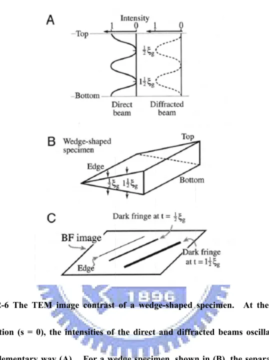
, (2-7) where n is obtain by counting the number n of dislocations and measuring the foil length l and foil thickness h in a cross sectional TEM image. The number of dislocations and foil length could be numbered and measured easily from the picture; however, the foil thickness has to be derived from thickness fringe in TEM image. From the Howie-Whelan equations, the intensity of Bragg diffracted beam can be written as [28]:
| | 1 , (2-8) where t is the z axial distance of intensity at the bottom of the specimen, Ig is the dark
field image intensity, φg is the amplitude of the diffracted beam for reflection G, seff is
the effective excitation error
, (2-9) with s being a measure of how far deviating from the exact Bragg condition, and the excitation being the characteristic length distance for the diffraction vector g and also named as extinction distance. The extinction distance can be described as:
, (2-10) where λ is the wavelength of electrons, Fg is the structure factor for the diffraction
vector g, Vc is the volume of a unit cell and θB is Bragg angle. If we neglect the
relativistic effects:
, , (2-11) 2 , (2-12) , (2-13) If take relativistic effects into account:
, 2 , (2-14)
, 1 , . (2-15)
Combining (2-12) into (2-15) gives:
, ; (2-16) Combining (2-14) into (2-16) gives:
2 , 2 ; (2-17) And combining (2-17) into (2-13) gives:
, (2-18)
where h is the Plank’s constant equal to 6.626 x 10⁻³⁴ Nms, p is the momentum of electron, charge e equals to -1.602 x 10⁻¹⁹ C, rest mass m0 = 9.109 x 10⁻³¹ kg, speed of
For acceleration voltage 200 kV, the relativistic wavelength is 0.0251 Å. For hexagonal ZnO operated at 200 keV, g = (0002), a = 3.2438 Å and c = 5.2036 Å, Eq. (2-4) gives θB=0.27689o, where θB is Bragg angle. The structure factor Fg of ZnO with
diffraction vector g = (0002) is F0002=11.564 Å and the volume of a unit cell
√
47.6199 Å3. Substituting these parameters into Eq. (2-10) gives 515.4 Å. Considering Eq. (2-8) for only one diffraction beam g, the two-beam approximation is applied. The two-beam condition means that we tilt the crystal so that there are only two strong beams exist. One is the direct beam and the other is the diffraction beam with s = 0. The rest of the diffracted beams are very weak (s >> 0 or << 0) and the contribution to is ignored. Then, Eq. (2-9) becomes
. Simplify Eq. (2-8), we have | | 1 , for t = 0 or t = n , Ig = 0 and for t = , Ig = 1. The oscillatory intensity variations with t are
illustrated in Fig. 2-6.
For hexagonal ZnO with two-beam condition g = (0002), t = = 257.7 Å for the first dark fringe. With given foil thickness, the dislocation density can be evaluated from the Eq. (2-7).
Fig. cond comp the f the e 2-6 The T dition (s = plementary fringes in th extinction d TEM imag 0), the int y way (A). he image, s distance, e contrast ensities of For a we shown in (C . of a wedg the direct edge specim C) is determ ge-shaped and diffra men, shown mined by t specimen. acted beam n in (B), th the angle of At the B ms oscillate he separati f the wedge Bragg e in a on of e and
2-4 Photoluminescence characterization
PL is a very useful and powerful optical characterization tool in the semiconductor industry, with its sensitive ability to reveal the emission mechanism and band structure of semiconductors. From PL spectra the defects or impurities can also be identified in the compound semiconductors, which affect material quality and device performance. A given impurity produces a set of characteristic spectral features. The fingerprint can be used to identify the impurity type. Often several different impurities can be found in a single PL spectrum. In addition, the line width of each PL peak is an indication of sample’s quality, although such analysis has not yet become highly quantitative.
PL is the optical radiation emitted by a physical system (in excess the thermal equilibrium blackbody radiation) resulting from excitation to a non-equilibrium state by irradiation with light. Three processes can be distinguished: (i) creation of electron-hole pairs by absorption of the incoming light, (ii) radiative recombination of electron-hole pairs, and (iii) escape of the recombination radiation from the sample. Since the incoming light is absorbed to create electron-pair pairs, the greatest excitation of the sample occurs near the surface; the resulting carrier distribution is both inhomogeneous and non-equilibrium. In attempting to regain homogeneity and equilibrium, the excess carriers will diffuse away from the surface while being depleted by both radiative and nonradiative recombination processes. Most of the excitation of
the crystal is thereby restricted to a region within a diffusion length (or absorption length) of the illuminated surface. Consequently, the vast majority of PL experiments are arranged to examine the light emitted from the irradiated side of the samples. This is often called front surface PL.
2-4-1 Fundamental Transitions
Since emission requires the system being in a non-equilibrium condition, some means of exciting energy is acting on the semiconductor to produce hole-electron pairs. We summarize the fundamental transitions, those occurring at or near the band edges as below.
1. Free excitons
A free hole and a free electron as a pair of opposite charges experience a coulomb attraction. Hence the electron can orbit about the hole as a hydrogen-like atom. If the material is sufficiently pure, the electrons and holes pair into excitons which then recombine, emitting a narrow spectral line. In a direct-gap semiconductor, where momentum is conserved in a simple radiative transition, the energy of the emitted photon is simply
hν = E
g – Ex ,
where E
g and Ex are the band gap and the exciton binding energy.
Similar to the way that free carriers can be bound to (point-) defects, it is found that excitons can also be bound to defects. A free hole can combine with a neutral donor to form a positively charged excitonic ion. In this case, the electron bound to the donor still travels in a wide orbit about the donor. The associated hole, which moves in the electrostatic field of the “fixed” dipole, determined by the instantaneous position of the electron, also travels about this donor; for this reason, this complex is called a “bound exciton”. An electron associated with a neutral acceptor is also a bound exciton. The binding energy of an exciton to a neutral donor (acceptor) is usually much smaller than the binding energy of an electron (hole) to the donor (acceptor).
3. Donor-Acceptor Pairs
Donors and acceptors can form pairs and act as stationary molecules imbedded in the host crystal. The coulomb interaction between a donor and an acceptor results in a lowering of their binding energies. In the donor-acceptor pair case it is convenient to consider only the separation between the donor and the acceptor level:
,
where r is the separation of donor-acceptor pair, E
D and EA are the respective ionization
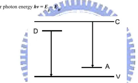
energies of the donor and the acceptor as isolated impurities. 4. Deep transitions
conduction band to an acceptor state or a transition from a donor to the valence band in Fig. 2-7. Such a transition emit a photon hν = E
g – Ei (Ei stands for ED or EA) for
direct transitions and hν = E
g – Ei - Ep if the transition is indirect and involves a phonon
of energy E
p. Hence the deep transitions can be distinguished as (1)
conduction-band-to-acceptor transition which produces an emission peak at hν = E
g –
E
A, and (2) donor-to-valence-band transition which produces an emission peak at the
higher photon energy hν = E
g – ED.
Fig. 2-7 Radiative transitions between a band and an impurity state
5. Transitions to deep levels
Some impurities have large ionization energies; therefore, they form deep levels in the energy gap. Radiative transitions between these states and the band edge emit at
hν = E
g – Ei. Some defects not only (or a few) levels close to one band, but have
several of levels partly around the middle of the gap. They give rise to the green, orange and red emission bands of wide-gap semiconductor such as ZnO and ZnS.
Chapter 3 Experimental details
3-1 The growth of ZnO films
3-1-1 Description of Laser-MBE system
The laser-molecular beam epitaxy (laser-MBE) growth system is also known as pulsed-laser deposition (PLD) and has been used to grow high quality films for more than a decade. The laser-MBE consists of two chambers, one is load lock chamber and the other is deposition chamber. The load lock chamber is a small spherical chamber with a Viton sealed quick access door for substrate loading. The substrate is mounted on a substrate holder. The substrate holder can be moved from the load lock into the deposition chamber by using a magnetically coupled transfer arm. By using the push-pull type pick-up manipulator equipped in the load lock module, substrates can be transferred from load lock to the deposition chamber. The deposition chamber, designed for pulsed laser deposition, is equipped with a target manipulator, a substrate holding and heating system, a pumping system, vacuum monitoring devices, necessary parts for laser inlet and a watching window.
3-1-22 The layouut of laser-MMBE systemm Th the g cham vacu pulse is sho he laser-MB growth cha mbers. A c uum pressure The ZnO t ed excimer own below. BE growth s amber, as s combination e (< 10-8 tor thin films w laser (Lamd Fig. 3-1 system cons shown in F n of scroll rr). were prepar da Physics Layout of l sists of two Fig. 3-1. pump and o chambers, There is a turbo pum the load lo a gate valv mp is used ock chambe ve between to achieve er and n two high red by the L LPX 210i). laser-MBE Laser-MBE . The deta E system E deposition ailed data sh n utilizing a heet of KrF a KrF laser
3-1-3 Target preparation
The target was prepared by commercial hot-pressed stoichiometric ZnO target with purity of 99.999% and the target size is 1’’ × 0.118’’. Before the deposition, the laser beam was shone on the ZnO target to remove the contamination on the target surface. 3-1-4 Preparation of substrate
The composite γ-Al2O3/Si substrate was prepared by advanced nano epitaxy
laboratory, NTHU, led by Prof. M. Hong and Prof. J. Kwo. The detailed preparation procedure of the substrate can be found in [29] and is also briefly described below.
Si wafers 2 inch in diameter with (111) as the normal to the wafer plane were put into
a multi-chamber MBE/ultrahigh vacuum (UHV) system [30], after being cleaned with a Radio Corporation of America (RCA) method and an HF dip. Si wafers were heated to temperatures above ~550 °C, and then transferred under an UHV (to eliminate any
high-purity sapphire (purchased from Maintech, Huntingdon, PA, with a purity of
99.99%) was employed as the Al2O3 source in this work. During the oxide deposition,
the vacuum in the chamber was maintained in the low 10−9 torr (even during the
evaporation of sapphire) and substrate temperatures were maintained at about 700–750
°C. After the deposition of Al2O3, the substrates (γ-Al2O3/Si) were cut into pieces of
an area of 1 × 1 cm2 for subsequent epitaxial growth of ZnO. Before transferring these
substrates into laser-MBE load lock chamber, each substrate was put in acetone solution and cleaned in a supersonic oscillator for 5 minutes to remove the particles on the substrate surface. After the surface treatment, the substrates were mounted on the substrate holder and loaded into the ZnO growth chamber.
3-1-5 Operating process of laser-MBE
(1) Load the mounted substrate holder into the load lock chamber and turn on the scroll pump.
(2) After the pressure of the chamber is pumped down to lower than 3 × 10⁻³ torr, then turn the turbo pump on.
(3) The pressure of the chamber should reach 10-9 torr in three hours. Only at this condition, we open the gate valve between the load lock and deposition chamber. We use the magnetically coupled transfer arm to transfer the substrate holder from the load lock chamber into the deposition chamber.
(4) After substrate transferred, close the gate valve.
(5) Adjust the distance between the substrate and ZnO target to reach the appropriate position.
(6) Make sure the water cooling system works properly.
(7) Turn on the thermal controller and power supply. Set the desired thermal program.
(8) Ensure the target substrate temperature is reached. Wait for a few minutes to let the chamber pressure decline to 3 × 10⁻⁸.
(9) Turn on step motor to start the mirror scanner. Turn on target manipulator and sample manipulator rotation to ensure the uniformed deposition.
(10) Turn on the laser and start the deposition.
(11) After thin film growth is completed, open the gate valve and use the magnetically
coupled transfer arm to retrieve the sample from the main chamber to the load lock chamber.
(12) Stop the turbo and scroll pump. When the blades of the turbo pump stop, we can
vent the load lock chamber by inserting N2 gas.
After surface treatment, the substrate was loaded in the chamber with the base pressure of 1 × 10⁻⁹ torr. We used a focused lens (f = 40 cm) to converge the laser beam through a viewpoint onto the target, which makes 45 degrees to the normal of the target. Inside the growth chamber, a ZnO ceramic target (99.999 % purity) was
located in front of the substrate holder at a distance of 5 cm and was ablated by a KrF excimer pulsed-laser with the wavelength, pulse duration, repetition rate, and laser fluence of 248 nm, 25 ns, 10 Hz, and 6 J/cm2, respectively. At the same time, the laser beam was scanned back and forth by moving a reflection mirror, which was driven by a stepping motor to prevent laser from hitting at the same spot on the target that leads to penetrate the target or non-uniform film growth. The substrate was heated with a halogen light bulb through the program temperature controller. The temperatures of the substrate holder were varied from 200oC to 500oC. The deposition of the ZnO thin films was carried out without oxygen flowing, under this circumstances, the pressure was maintained at 1 × 10⁻⁹ torr during deposition. The typical growth rate and sample thickness were 0.42 Å /s and ~300 nm, respectively.
3-2 Structural characterization of the ZnO films
3-2-1 X-ray diffraction
The crystal structure of ZnO films was inspected by XRD measurements which were performed with a four-circle diffractometer at the beamlines BL17A and BL13A of National Synchrotron Radiation Research Center, Taiwan, with incident wavelength 1.3344 and 1.023 Å, respectively. Two pairs of slits, located between the sample and a NaI scintillation detector, were employed and yielded a typical resolution of 4 × 10⁻³ Å−1.
3-2-2 Cross sectional TEM
Cross sectional TEM images and SAED patterns were taken using a field-emission-gun type TEM (Philips TECNAI-20) operated at 200 keV. For the preparation of cross-sectional TEM specimens, several steps of lapping and polishing are required. Figures 3.2(1) – (4) shows the specimen preparation processes. The first step of the preparation was a mechanical treatment of the materials, like sawing or punching to give the sample a square form with approximately 3 × 3 mm. Second, we glued the sample to a silicon substrate to form a formation of sandwich, as show in Fig. 3-2(2). Third, we polished the sandwich-like specimen by a polishing machine. We observed the specimen by an optical microscopy (OM) to see if there occurred a Newton’s ring in the specimen after polishing. If there existed Newton’s ring and showed no cracks in the OM image of the specimen, the thickness of specimen was proper for the cross sectional TEM measurement. Finally, the specimen was mounted on a copper ring, as shown in Fig. 3-2(4), and can be loaded into the TEM measurement holder.
3-3
3-3-1 A utiliz refle We photo The n Fi spMeasur
1 Photolum He-Cd las zed as a pum ction mirro utilized tw o-multiplier normal oper ig. 3-2 A sch pecimenrements
minescence er (Kimmo mping sourc ors, focusin wo single-r tube (PM rating volta hematic shof optica
detection s on IK5552R ce for PL. ng and coll -grating m MT) which i age of PMT howing the pal prope
system R-F) operat Figure 3-2 lecting lens monochroma is matched is 0.8 kV.preparation of a crosss-sectional TEM
rties
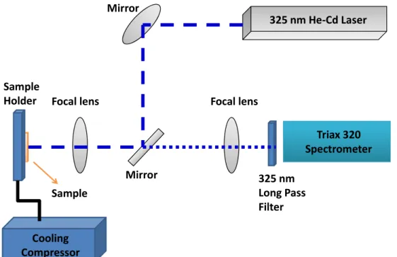
ing at 325 2 depicts the s, sample h ators (Triax with a ph Moreover nm UV lin e PL system holder and x 320) eq oton counte r, we used fl ne is comm m setup inclu cooling sy quipped wi er for detec fluorescent l monly uding ystem. ith a ction. lampsto calibrate spectral response of the spectrometer and detector. Each PL signal was collected for about 0.1 second at a step of 0.1 nm, and the data were transmitted through a GPIB card and recorded by a computer. The monochromator was a 32 cm long with three available resolutions of lines 600, 1200 and 1800 grooves/mm, respectively. When the entrance and exit slits were both opened at about 50 μm, the resolution was about 0.1 nm in this system. Low temperature PL measurements were carried out by collecting the sample using a closed cycle cryogenic system.
325 nm He‐Cd Laser Triax 320 Spectrometer Cooling Compressor Mirror Mirror Focal lens Focal lens 325 nm Long Pass Filter Sample Holder Sample
Chapter 4 Results and Discussion
4-1 Results of X-ray measurements
4-1-1 Growth temperature dependent crystallinity of the ZnO films
ZnO films were deposited at a substrate temperature ranging from 200 to 500oC. Two batches of samples were grown on two composite substrates, which were prepared nominally under the same deposition conditions.
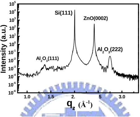
2 3
Figure 4-1 illustrates the radial scan along surface normal of the ZnO film grown at 300oC, where the abscissa qz = 4πsinθ/λ denotes the momentum transfer along the
surface normal and λ is the incident x-ray wavelength. According to JCPDS (Joint Committee on Powder Diffraction Standards), the three pronounced peaks are assigned as the (0002) reflection of wurzite ZnO, (222) peak of cubic γ-Al2O3 and (111) peak of
cubic Si, elucidating the cube-on-cube growth of γ-Al2O3 on Si and a crystalline
orientation relationship of along surface normal. The pronounced thickness fringes observed near the γ-Al2O3(222) reflection indicates the
sharpness of the γ-Al2O3 interfaces; the fringe period yields a layer thickness of ~15.3
nm. From the FWHM of the γ-Al2O3(222) reflection, we derived the vertical
coherence length of the buffer layer, using the Scherrer’s equation, to be ~15 nm, which is close to the layer thickness. This implies that the structural coherence of the buffer
ZnO γ-Al O Si
layer is maintained over almost the entire layer thickness.
Azimuthal cone scans (φ-scans) across the off-normal ZnO{1010}, γ-Al2O3{440},
and Si{220} reflections, as shown in Fig. 4-2, were measured to examine their in-plane epitaxial relationship. Six ZnO diffracted peaks evenly spaced 60o apart confirmed that ZnO film with a six-fold rotational symmetry against surface normal was grown epitaxially on the γ-Al2O3/Si(111) composite substrate. Furthermore, two sets of peaks
with 3-fold symmetry were observed in the γ-Al2O3{440} φ-scan, revealing the
cube-on-cube growth of γ-Al2O3 on Si and the coexistence of two in-plane rotated
variants. The dominant one has the same angular position as that of the Si{220}, A-type (111) orientated domain, and the minor one has its in-plane orientation rotated 60o from that of Si substrate, B-type domain [32]. These results suggest that the in-plane epitaxial relationship of this hetero-epitaxial system follows {1010}ZnO ||
2 3
-Al O
{224}γ or {422}γ-Al O2 3 || {224}Si. In this geometry, the two-dimensional
hexagonal unit cell of the γ-Al2O3(111) plane is aligned with the ZnO basal plane
having its lattice constant equal to √2·a(γ-Al2O3) = 11.186 Å, about 3.45 times larger
1.0 1.5 2.0 2.5 3.0 10-6 10-5 10-4 10-3 10-2 10-1 100 101 102 103 104 105
Inte
ns
ity
(a
.u.)
q
z Al2O3(111) Si(111) ZnO(0002) Al2O3(222)(Å
-1)
Fig. 4-1 Radial scan along the surface normal of a 300 nm thick ZnO layer grown on γ-Al2O3/Si(111) composite substrate
0 60 120 180 240 300 360
Intensity (a.u.)
Φ
(deg.)
γ-Al2O3 {440} ZnO {1011} Si {220}Within the employed growth temperatures, all the samples exhibit the same structural characteristics with a small variation of less than 0.2% in ZnO lattice parameters. The lattice parameters of ZnO bulk are a = 3.2438 Å and c = 5.2036 Å, derived from the XRD data of a ZnO wafer. As compared with the lattice parameters of the grown ZnO films, we found that all the ZnO films experience a tensile strain (~0.28%) in the lateral direction and correspondingly a compressive strain (~0.19%) along the surface normal. To characterize the structural quality of the film under different growth temperature, the θ-rocking curve of ZnO(0002) reflection was performed. The small values of FWHM, varying between 0.32o and 0.61o with the minimum obtained at 300oC, manifest good crystalline quality of ZnO epi-layer even for such a thin film with thickness of ~0.3 μm. This value is as good as that of the ZnO epi-film grown on non-oxide buffer layer, such as ZnS [33], Al [34] and 3C-SiC [35]. The FWHMs of φ-scans across the off-normal ZnO(1010) reflection fall between 1.4o and 3.8o. It is worth noting that for the ZnO epi-layers grown on γ-Al2O3/Si(111) under different growth temperatures, those have smaller FWHM of
(0002) θ-rocking curve always have larger width in φ-scans across the off-normal )
0 1 0 1
( reflection, as shown in Fig. 4-3(a) and (b). This is different from ZnO grown on other substrates, such as c-plane sapphire, where both FWHMs always exhibit the same trend of increase/decrease with growth conditions [36]. Furthermore, we grew
ZnO film on two batches of buffer layers and found the structural quality of ZnO is sensitive to the structural perfection of γ-Al2O3 buffer layer. The FWHM of θ-rocking
curve of γ-Al2O3(222) of the first and the second batches are 0.023o and 0.024o,
respectively, while the FWHM of φ-scan across the off-normal γ-Al2O3(440) reflection
are 3.97o and 4.27o for the first and the second batches, respectively. The quality of buffer layer of the first batch is better than that of the second batch. The ZnO films grown on the first batch are found averagely better than that of the second batch, especially for the FWHMs of φ−scan of ZnO(1010). Nevertheless, the opposite trend of variation in Δθ and Δφ observed in both batches of samples. The factors, Δθ and Δφ are associated with different types of structural defect and the opposite variation trend of Δθ and Δφ allows us to identify their influence on the optical properties of ZnO film, which will be discussed later.
200 250 300 350 400 0.35 0.40 0.45 0.50 0.55 0.60 0.65 0.70
Δθ
(0002)ΔΦ
(1011)Δ
θ
(deg.)
Growth tem
p.
(oC
) 1.68 1.72 1.76 1.80ΔΦ
(deg.)
(a)Fig. 4-3(a) Correlation between growth temperature and ZnO Δθ(0002) / ΔΦ )
0 1 0 1
( distribution for the first batch of substrate
200 250 300 350 400 450 500 0.42 0.44 0.46 0.48 0.50 0.52 0.54 0.56 0.58 0.60 0.62
Growth temp.
(oC
) 3.0 3.2 3.4 3.6 3.8 4.0Δθ
(0002)ΔΦ
(1011)ΔΦ
(d
eg
.)
Δ
θ
eg.
(d
)
(b)4-1-2 Analysis of threading dislocation density by XRD
The major defect structure in the ZnO film is TDs. In our case, the majority of TDs have their lines lying along the [0001] growth direction that is the same as the ZnO film grown on commonly used c-sapphire [34]. For a (0001)-oriented thin film with wurtzite structure, the TDs are classified into three different types according to the direction of the corresponding Burgers vector (b) relative to the [0001] line direction. They are edge, screw and mixed TDs characterized with bE = 1/3⋅<1120>, bC = <0001>
and bM = 1/3⋅<1123>, respectively, where bM is the mix of bE and bC. In order to
address the defect structures of wurtzite ZnO by XRD, rocking curves of the ( 0 0)h h and (000l) reflections were measured. Note that the broadening of and (000l) rocking curves are associated with the lattice misalignment along the in-plane and growth directions, respectively. In other words, pure edge TDs twist the surrounding ZnO lattice about [0001], leading to the formation of vertical grain boundaries [37, 38, 39] and the crystalline planes are distorted. On the other hand, pure screw TDs tilt the ZnO lattice and generate a pure shear strain field [40], causing the (000l) planes being deformed. Thus, we measured the and (000l) reflections to investigate the influence of edge and screw TDs, respectively. The FWHMs of the
θ-rocking curves of (000l) Bragg peaks reflect the lattice twist/tilt and the line width of their radial scans are related to the lateral/vertical inhomogeneous strain field
/ ( 0 0)h h ( 0 0)h h ( 0 0)h h ( 0 0)h h
and domain size.
To obtain a quantitative results, we employed the Williamson-Hall (WH) plot (Δq vs. q, where q = 4πsin(2θ/2)/λ denoting the scattering vector andΔq is the line width in q along the radial direction) to separate the reflection peak broadening due to finite structural coherent length from strain-induced broadening. According to Eq. 2-6, the inverse of the ordinate intercept yields the coherence length which corresponds to the effective domain size and the slope yields the root-mean-square (rms) inhomogeneous strain. Figures 4-4 (a) and (b) are the typical WH plots of radial scans along the ZnO (h0h0) and (000l), respectively. For ZnO film grown at 300oC, the coherence length along surface normal is ~293.6 nm, indicating its structure maintains coherent almost over the entire film thickness. The in-plane domain size is 117 nm. The average lateral strain is ~3.83×10⁻³ about three times that along the surface normal (~1.3×10⁻³), indicating that the dominant cause of ZnO lattice distortion comes mainly from edge dislocation. Figures 4.5 (a) and (b) are plots of Δqt vs. q (where Δqt = q·Δθ denotes the
spread of θ in the transverse direction) for θ−rocking scans across the (h0h0) and (000l), the slopes yield the spread of twist and tilt angles, respectively. The twist angle (αΦ) and tilt angle (αΩ) of ZnO fall within the ranges of 1.38o~3.8o and 0.28o~0.53o,
respectively. Note that for samples grown under different temperatures, the ZnO films exhibit the opposite trend of variation for tilt and twist angles, which are similar to the
trend of θ−rocking curve linewidths of ZnO(0002) and (1010) reflections because
Δθ(0002) and Δφ(1011) bear the same physical meaning as the tilt and twist angles. The
TD density can be estimated from the corresponding Burgers vectors and tilt or twist angles. The density of screw type dislocations, Ns, is obtained using the equation: , where αΩ
is the tilt angle and bC is the magnitude of the corresponding
Burgers vector bC, which is [0001] with bC = 0.519 nm in our case [41]. The edge
type TD density, NE, can be calculated by adapting , where
α
φ , bE and Lare twist angle, the length of corresponding Burgers vector (bE = 0.325 nm) and
correlation length along the in-plane direction, respectively [39]. This formula is based on the model of dislocation piling up in small angle boundaries and forming subgrains with an average size L along the in-plane direction. As for our ZnO films grown at different temperatures, it is noticed that the density of edge TDs (1.39~9.97×1010 cm-2) is about 10 times higher than that of screw TDs (2.14~5.75×109 cm-2). Thus, the dominant type of dislocation of ZnO grown on γ-Al2O3/Si(111) is
edge TDs. It is the same as the case of ZnO grown on c-sapphire [36].
2 2 4.35 S C N b αΩ = 2.1 E E N b L αΦ =
0 2 4 6 8 10 0 10 20 30 40 50 (3030) (2020) (1010) 2nd batch
}
200 300 400 200 300 400Δ
q
[x10
-3 ]q
}
1st batch(Å)
0 1 2 3 4 5 6 0 20 40 60 80 100 120 (0004) (0002)}
}
1st batch 2nd batch 200 300 400 200 300 400q
Δ
q
[x10
-4 ] (a) (b)(Å)
Fig. 4-4 Williamson-Hall plots of ZnO layers grown at various temperatures. The symmetric radial scans were measured for (a) (h0h0) surface peaks and (b) (000l) normal reflections. Lines are linear fits of the data.
0 1 2 3 4 5 6 7 8 0 1000 2000 3000 4000 5000 6000 (3030) (2020) (1010)
}
}
1st batch 2nd batch 200 300 400 200 300 400q
Δ
q
t [x10
-4 ](Å)
(a) (b) 0 1 2 3 4 5 6 0 100 200 300 400 500 600 (0004) (0002)}
}
1st batch 2nd batch 200 300 400 200 300 400q
Δ
q
t [x10
-4 ](Å)
Fig. 4-5 A Δqt vs. q plot, an analogy to the WH plot for transverse scans, across
(a) surface peaks and (b) normal reflection
4-2 Structural characterization by TEM
4-2-1 cross sectional TEM
Illustrated in Fig. 4-6 (a) is a selected area electron diffraction (SAED) pattern along
Si
[112] direction. The diffraction peaks from Si substrate, γ-Al2O3 buffer and ZnO
epi-layer can be well identified and confirmed. The crystalline orientation relationship is (0002) || (222)ZnO γ-Al O2 3|| (111)Si at surface normal direction and
2 3
ZnO -Al O Si
0} || {440}γ &{220}
{112 at in-plane direction that are consistent with the results from XRD observation. Figure 4-6(b) is the high magnification TEM image taken at the interfacial region with [112] projection. It reveals unequivocal Si interfaces of ZnO/γ-Al2O3 and γ-Al2O3/Si; no intermediate layer was observed in either
interface. These results demonstrate that the growth of high-quality epi-ZnO film on Si by using a γ-Al2O3 buffer layer is achievable and the buffer serves as a good template
Fig. 4 cross proje 4-6 Selecte s-sectional ection (b). (b) ed area ele HR-TEM The inset 2 3
γ-Al O
ZnO
Si
ectron diffr micrograp is the corr 3 raction pat ph taken n responding γ-Al O2 3 (222) (0002 Si (220) ttern along ear the int SAED alon Si (111) ZnO 2) (0 Zn (1011) g [112]Si p terfacial re ng [101]Si ZnO (100) Si (111) 000) nO projection ( egion with direction. (a) and [101]Si4-2-2 Analysis of threading dislocation density
The types of dislocations in ZnO films were further characterized by cross-sectional TEM under a two-beam contrast condition. The diffraction contrast of dislocations in
TEM images arises from the bending of lattice planes caused by the dislocation induced strain field. For pure screw dislocations, planes with their normals perpendicalar to the Burgers vector bC are undistorted. Therefore, all electron beams that are diffracted by
planes containing bC show no image contrast. With g being the operating diffraction
vector, and bC the Burgers vector of the dislocation, the invisibility criterion for pure
screw TDs is g • bC = 0. For pure edge dislocations, only lattice planes perpendicular
to the dislocation line direction will be undistorted and edge dislocations will be invisible in images that are formed using electron beams diffracted from these planes. A pure edge dislocation gives rise to two displacement components of lattice. One is parallel to the Burgers vector bE, and the other perpendicular to the slip plane, those
normal can be expressed by bE × u with u denoting the unit vector along the positive
direction of the dislocation line. Therefore, to ensure complete invisibility for an edge dislocation, in addition to g • bE = 0, the condition g • (bE × u) = 0 has to be satisfied,
too [27]. Based on these invisibility criteria, we can distinguish the types of the TDs by analyzing images taken with different operating diffraction vector g. Figures 4-7(a)-(c) show the images of the ZnO film grown at 300oC taken with the diffraction
vector g equal to ZnO(0002), (1120), and (1122), respectively. According to the invisibility criteria, g • b = 0, screw type dislocations with bC = <0001> are invisible
with g =(1120) but visible under g = (0002) and (1122). In contrast, edge type dislocations with bE = 1/3⋅<1120> and (bE × u) // <1100>should be invisible under g
= (0002) but visible under g = (1120) and (1122). As to the TDs of mixed type character with bM = 1/3⋅<1123>, they are visible under all three g vectors. In all
three micrographs, TDs are seen as dark lines stemming from the ZnO/γ-Al2O3 interface
with their dislocation lines primarily along the [0001] direction. The dislocation density, D, was determined by formula, D = n/lh, where n is the number of dislocations, l is foil length and h is foil thickness. The foil thickness was determined by measuring the number of extinction distance fringes in two-beam images (g = (0002)) and using the extinction distance as a reference to derive specimen thickness. We calculated the densities of edge, screw and mixed TDs to be approximate 1.04×10¹⁰ (~ 27%), 3.46×10⁹ (~ 10%), and 2.42×1010 cm-2 (~ 63%), respectively. Thus, about 90% of total TDs contain the edge component consistent with the result calculated from XRD data that edge is the dominant type TDs.
G=(1120)
G=(1122)
G=(0002)
‐
‐
(a)
(c)
(b)
Fig. 4-7 Two-beam bright field cross sectional micrograph of a ZnO thin film taken
4-3 Optical characterization by PL
4-3-1 Photoluminescence spectra of as-grown films
We carried out low temperature (LT) PL at 15K to characterize the optical properties of the ZnO films. The PL spectra of ZnO films are shown in Fig. 4-8. Regardless
of the growth temperatures, the main features on PL spectra are common for all samples. The spectra can be divided into two parts: sharp near band-edge emission (NBE) and broad deep level emission (DLE), which are centered at ~3.365 and ~2.196 eV, respectively. The dominant peak at NBE region is attributed to the recombination of excitons bound to neutral donor (DoX) [42] and the broad DLE results from point defects such as O vacanciesand Zn interstitials [43]. The assignments of NBE peaks are also shown in Fig. 4-9, which is the PL spectrum of the ZnO grown at 300oC. The peak at 3.375 eV was designated as the free A-exciton (FXA) line; the binding energy of
the corresponding A-exciton was obtained to be 58.875 meV by fitting the temperature dependent PL data using the Arrhenius expression, as shown in Fig. 4-10. The dominant peak at 3.364 eV in the NBE region was assigned to the recombination of excitons bound to neutral donor (DoX) [44] and its FWHM is 9.4 meV. The DoX emission accompanied with single phonon (DoX–1LO) and dual phonon (DoX–2LO) replica appear at 3.288 and 3.215 eV. The peak at 3.23 eV is attributed to the donor–acceptor pair (DAP) transition. Another strong line at 3.328 eV originates from