Optical Properties of Hydrogenated Amorphous Silicon
Gwo-Jen Jan (B Bl ?&l>
Department of Electrical Engineering, National Taiwan University, Taipei, Taiwan 10764
and
Ying-Sheng Huang ( Z !$Z B >
Department of Electronics Engineering and Technology, National Taiwan Institute of Technology Taipei, Taiwan 10772
(Received 10 May 1935)
An on-line microcomputer based rotating light pipe reflecto-meter (RLPR) has been set up. Using this system we have in-vestigated the optical properties of hydrogenated amorphous silicon semiconductor materials. The experimental results of reflectivity R(w) has been analyzed by the Kramers-Kronig method. The complex dielectric function e (o) and the effective number of electron per single Si-atom have been calculated. The results show that Boron-doped hydrogenated amorphous silicon and thermal annealing improved the crystallinity.
I. INTRODUCTION
The. amorphous silicon (a-$) has been the subject of many investigations on disorder system over the past 15 years. The amorphous forms of this single elemental semiconductor is chosen because. of the throughly characterized and relatively well-understood crystalline properties. However, a-Si film generated made by sputtering (1) or electron beam techni-ques (2) contain a large density of states in the dangling bonds (l), and resulting large density of states in the energy gap makes it very difficult to move the Fermi level.
W. E. Spear and P. G. Le Combere (3) haved observed that glow discharged-produced a-Si possessed a relatively low density of gap states as compare to sputtered or evaporated film. It is now clear that these films are actually a amorphous silicon alloy and currently refered to as hydrogenated amorphous silicon (a-Si:H) films. The density of states in the energy gap of a-Si:H is relatively low, and thus the Fermi level can be moved with respect to the band edges by adding small quantities of certain dopants such as boron and phosphorous (45) as well as arsenic (7) have reported that the hydrogen evolution and annealing behavior is strongly modified if addtional structure defects are present due to boron doping.
The sharp features in the optical spectral of semiconductors are determined by long range order and hence are quite sensitive to disorder. The most of optical investigations have been confined to the region around the absorption edge (l-3 eV), (8,9). The
di-19
20 OPTICAL PROPERTIES OF HYDROGENATED AMORPHOUS SILICON
electric functions and optical parameters of elemental and III-V alloy semiconductors have been studied by Aspnes (10) et al. using the spectroscopic ellipsometer. The optical pro-perties and damage analysis of GaAs single crystals partly amorphous by ion implementation were studied by the same technique (11). Unfortunely, spectroscopic ellipsometer can only provide the information of the optical properties in the energy range 1 .O-6-.0 eV. In con-strast only a few results about the intensive studies on the gap states above the ultraviolet (UV) have been reported. Therefore, the reflectance spectroscopy over the wide energy range (0.8- 10 eV) will provide a considerable important tool to investigate thr properties of amorphous semiconductor.
Weiser et al. (12) have studies the reflectivity and the imaginary part of the dielectric function e2 over the photon energy range l-l 0 eV of glow-discharge silicon fabricated under different conditions. A broad bump, featureless in the imaginary part of the di-electric function e2 spectrum has been reported. The effects. of laser annealing on ion-damage silicon have been investigated by Aspnes (13). He found the energy features in e2 can be associated with crystalline silicon. Thus, the optical properties in UV region arise from the transitions between the band structure. These transition response is due to . structure changes and/or randomly distributed impurities.
In order to study the boron doping and high temperature thermal annealing effect of a-Si:H samples, we have set up an automatic rotating light pipe reflectometer to measure the reflectivity spectral of the samples. The imaginary part of the dielectric function is cal-culated by the Kramers-Kronig analysis. The effective electron number per Si atom is also calculated from the dielectric function. In this paper the results of high temperature thermal.annealed as well as unannealed a-Si:H(B) are reported. The detail structure in e2 of these samples will provide the information of the crystallinity improvement of silicon. For , comparison we have also carried out the reflectance spectrum of the crystalline silicon.
II. THEORETICAL CONSIDERATION
The linear response of non-magnetic solid with isotropic or cubic symmetry to incident photon can be described in terms of two optical constants. These two optical constants (e1 , e2 ) or (n, k) are related by the Kiamers-Kronig dispersion relations. It is more useful to express the dispersion relation between r, the magnitude of R, and the phase angle 8 (w):
T(W) = R(w)exp[ie(w)] (1)
l9 (W)=WPJ= [ lnR(W’)-lnR(w)] dw
IT 0 cd2 - o’2
(2)
where r is a complex reflection coefficient and 0 (w> is the phase angle. The two optical constants n and k can be obtained fron R(w) and e(w) by the following relations:
n ( W ) = 1 - R
1 +R-2J&ose (3)
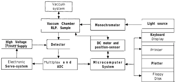
-22 OPTICAL PROPERTIES OF HYDROGENATED AMORPHOUS SILICON Vaccum system
s ,
I , Vaccum Chamber RLP. Sample Monochromator Llght source I I I f + & Keyboard Hlgh Voltage DisplayPower Supply Detector DC motor and i posltlon-sensor 1 --+ Printer $ Electronic
Servo-system - Multiplex a n dADC _ M l c r o c o m p u t e r _System Plotter
--+ F~~PDY
Disk
FIG. 1 Schematic functional block diagram of automatic RLPR System
hydrogen arc lamp is used in the VUV and UV region. A 150 watt Xenon arc lamp is used . in the UV and visible light region. The Halogen Tungstan fused quartz lamp is used in the visible and near infra-red (IR) light range. The optical components and electro-optical devices used in our system is listed in table I.
TABLE I: E-O and Optical components related to measuring wavelenght
ssoo- 1 2 0 0 0 2 5 0 0 - 9 0 0 0 I300 - 3 5 0 0
Light Source Tunqstan Ouartz L a m p 150 Watt I K Watt Xe - Arc Lamp tiyarogen Arc LanD omractlon
Grating 6 0 0 1200 2 4 0 0
Grove Denslty(G/mml D l r r r a c t l o n
, I I
Vaccum I * IO-b tow
5ystem NO No Yes
The photon detectors used in our measurement are Hamamatsu photomultiplier tube (PMT) S-l and S-20. The S-l PMT is used for the photon energy lower than 3.0 eV and S-20 PMT is used over the photon energy of 1.5 to 5.5 eV. The front surface of the rotat-ing light pipe (fuse quartz of supersil no. 1) is coated with the phosphorus (usrotat-ing sodium salicylate phosphorus) and S-20 PMT is used over the photon energy of 3 eV to 9.5 eV. The chamber is mounted inside the vaccum working chamber. The chamber is pumped
down to 1 * 10” torr for VUV region. The schematical block diagram of rotating light pipe set up is shown in Fig. (2). The absolute accuracy of reflectivity R(w) in our measurement system is around 2% but the relative accuracy of R(w) value is around 0.3%.
R o t a t l n g speed i
(a) Side vlew of rotatlng light pipe
r________---- _______________________--- e____-.
Vaccum c h a m b e r :
(Ph1O-6 torr) !
Rotating light pipe
: Torold mirror i ( MgFz coating 1 Monochromatlc llght source : __--- ____________________________-____---. (b) T o p V i e w O f geometriCal arrangement
FIG. 2 The schematical block diagram of rotating light pipe set up
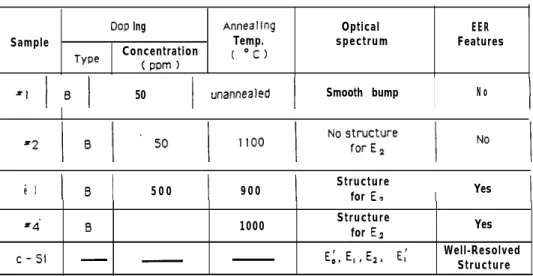
The samples used in this experiment were prepared by the glow-discharge technique. The chaiacteristics and prepartion conditions are summarized and listed in table II. All samples are boron-doped a-Si:H alloy except c-Si. The doping concentration and annealing temperature are listed at the second and third column of table II. The samples have been annealed at temperature of w 1000” C for about 10 Min.
TABLE II. Summary of preparation condition for a-Si:H samples and experimental results
00~ Ing Annealing Optical EER
Sample Temp. spectrum Features
Type Concentration ( OC)
( pm 1
/ ft j B 1 50 / unannealed / Smooth bump
I
NoI I I Structure ‘ 3 B 5 0 0 I 9 0 0 I for E, I Yes I 24 0 cs1 -1000 Structurefor El E:, E,, El. E:
Yes Well-Resolved
24 OPTICAL PROPERTIES OF HYDROGENATED AMORPHOUS SILICON IV. EXPERIMENTAL RESULTS AND DATA ANALYSIS
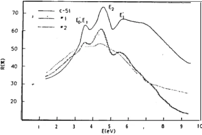
We have measured the reflectivity of c-Si and a-Si:H(B) samples at room temperature carried out by our measurement system. The experimental results are shown in Fig. (3) and Fig. (4). The imaginary part of the dielectric function is calculated from the measured
I 2 3 4 5 6 , 8 9 IO
E(eV) .
FIG. 3 The reflectance spectra for high temperature annealing a-Si:H(B), unannealed a-Si:(H) and c-Si.
I I I I I
I 2 3 4 5 Q : :, gl
E(eV)
FIG. 4 The’reflectance spectra for high temperature annealing a-Si:H(B), and c-Si.
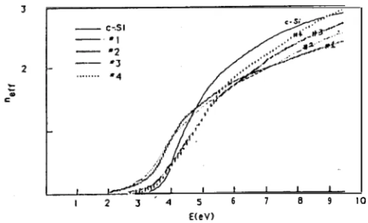
reflectivity spectrum using Kramers-Kronig analysis and shown in Fig. (5) and Fig. (6). The effective electron number per single Si-atom is calculated from the imaginary part of the dielectric function e2 and shown in Fig. (7).
In Fig. (3) shows the reflectivity spectra of the unannealed and high temperature thermal annealed boron-doped with 50-PPM concentration as well as c-Si. The e2 spectral of those samples are shown in Fig. (5). The reflectivity and e2 spectra of the c-Si agree closely with Philip’s results (1 S- 17). The reflectance and the e2 spectra of the unannealed boron-doped a-Si:H sample shows a featureless broad bump spectra. This is similar to Weiser’s result (12, 18). The samples of the high temperature thermal annealed a-Si:H(B) shows the little optical feature at Eb, E, and E; transition not well resolved feature at E2 in
e2 spectrum.
FIG. 5 The imaginary part e2 (E) of the dielectric function for high temperature annealing a-Si:H(B), un-annealed a-Si:H(B) and c-Si.
4 0 - c-51 - ‘5 - - 4 IO w” 2 0 IO . I 2 3 4 S 6 7 0 Y 10 E(cV)
FIG. 6 The imaginary part e2 (E) of the dielectric function for high temperature annealing a-Si:H(B), and c-Si.
S 6 7 6 9 IO
FIG. 7 The effective number of electron per atom contributing to opfical absorption.
Figure (4) and Fig. (6) show the reflectance and E 2 spectra of the high temperature thermal ahnealed a-Si:H with heaviv boron-doped alloy. In Fig. (5) presents the little
--..--26 OPTICAL PROPERTIES OF HYDROGENATED AMORPHOUS SILICON
optical features at EL, E, transition resolved features at EZ and E; energy position.
Figure (7) shows the effective electron number per single Si-atom calculated from the imaginary part of the dielectric function. The experimental results are summarized in table II.
V. DISCUSSIONS AND CONCLUSION
The most striking observation by comparing the optical spectra of a-Si and c-Si is the complete loss of fine structure in the disordered state. The fine structure is related to the singularities of the band structure and depends quite sensitive on the long range order in the material. These features are broaden rapidly with the loss of long range order (12). The featureless broad bump in E 2 spectrum will present in amorphous state due to the short range order. The fine structure in reflectivity and e2 spectra show the more informations about the crystalline state. The imaginary part of the dielectric function provide the detail-ed information about the crystalline improvement of the a-Si:H alloy.
.
No fine structure in ez spectrum is found in the sample #I. It indicates that the unannealed a-Si:H alloy with low concentration of boron-doped exhibits the amorphous state. The reflectivity and e2 spectra of the sample #2 show the fine structure at Eb , E, and E; transition but not well resolved fine structure at E2 transition. It presents the short range order rather than the long range order. The crystallinity of a-Si:H(B) improved by the high temperature thermal annealing. This results have shown by the report of R. Tsu et al. using Raman characterization technique (19).
The reflectance and e2 spectra of samples #3 and #4 show the fine structure at critical points clearly. These optical features are from interband transition at the critical points. The annealing temperature of samples #3 and #4 are the same as sample #2 except the higher concentration of boron impurity. W. Beyer et al. (7) have shown the structure defecs can be modified by the thermal annealing and/or boron-doped. Electrolyte electrore-flectance (EER) technique is a powerful tool to determine the optical transitions at critical point rapidly (20-2 1). When we check the EER spectrum of our measured samples, we found only sample #3 and #4 presented the EER energy features. But these features are not as fine and narrow as c-Si sample.’ This evidences support that the high terpeiature thermal annealing and heavily boron-doped will improve the crystallinity of a-Si:H alloy. The major difference between samples #3 and #4 and c-Si is the El , Eb features which are greatly depressed in the former materials. This effect may be related to the presence of a large number of free carriers. Aspnes (13) has also found that a depression of the 3.4 eV structure relative to Ez in heavily-doped silicon. Our results indicate the high temperature thermal annealed and heavily boron-doped a-Si:H alloy is sufficient to obtain a high degree of structure order. This result is quite different compared with heavily n-doped hydro-genated’ and fluorinated amorphous silicon (a-Si:F:H) alloy which formed the microcry-stalline structure (2 1).
should also alter the optical transition elements. These changes are repsonsible for the large variation of the height of the peak (7). Thus we calculated the effective number neff (0) of electrons per single Si-atom excited at given photon energy h&. For c-Si neff rises deeply above the direct energy band gap near 3 eV and saturated outsidevthe range plotted here between 16 to 20 eV at a value of 4 corresponding to the 4 valence electron (20). The lower value of neff can be due to decreasing optical transition matrix element. The same observation has been reportqd by Bauer (23) for c-Si and .amorphous germanium. He in-terpreted the lack of oscillator strength as an increasing localization of the deeper valence states in the disordered solid. The sample #1 exhibits the amorphous phase and has the lower value of the neff than samples #2, #3, #4. The neff value of the sample #2 is be-tween that of samples #l and #3. That means the crystallinity of the samples #3 and #4 is better than #l and #2. The’dopant of bbron may play an important role in a-Si:H alloy as well as high temperature thermal annealing process.
ACKNOLEDGEMENT
.
We would like to thank professor Fred H. Pollak at the physics department of the Brooklyn college of the City university of New York to provide the samples and facilities of the VUV range measurement. We also like to acknowledge the National Science Council supported this research project under contract no. NSC-73-0204-M002-02 and NSC-74-020%M1002-19.
REFERENCES
1. M. H. Brodsky and R. S. Tittle, Phys. Rev. Lett. 23, 581 (1969). 2. D. Beaglehole and M. Zavetova, J. NonCryst. Solids 4, 272 (1970). 3. W. E. Spear and P. G. Le Comber, Solid State Commun. l,7, 1193 (1975). 4. W. E. Spear and P. G. Le Comber, J. Non-Cryst. Solids &la, ,727 (1972). 5. D. E. Carlson, U. S. Patent No. 4,064 521 (1977).
6. J. C. Knights, J. M. Hayes, and J. C. Mikkelsen, Jr., Phys. Rev. Lett. -39, 712 (1977). 7. W. Beyer and H. Wagner, J. of NonCryst. 59-60, 161 (1963).
8. G. E. Jellison and F. A. Modine, Phys. Rev. (B) 27,7466 (1983).
9. W. B. Jackson, D. K. bieglesen, R. J. Nemanich and J. C. Knights, Appl. Phys. Lett. 42, 105 (1983).
10. D. E. Aspnes and A. A. Atudna, Phys. Rev. (B) 27,985 (1983).
11. M. Erman, J. B. Theeten, P. Chambon, S. M. Kelso, and D. E. Aspnes, J. Appl. Phys. 56,2664 (1984).
12. G. Weiser, D. Ewald, and M. Milleville, J. of Non-Cryst. Solids 35-36, 447 (1980); Phil. Mag. B40, 29 1 (1979).
28 oPTI~ALPR~PERTIES~FHYDR~OENATEDAM~RPH~USSILIC~N 14. 15. 16. 17. 18. 19. 20. 21. 22. 23.
Materials, eds. C. L. Anderson, G. K. Cellar and G. A. Rozgonyi, (Electro-ChemicaI Society, Princeton, 1980) pp. 414.
See, for example, M. L. Theye in Optical Properties of Solids - New Developments, ed. by B. 0. Seraphin (North Holland, N. Y., 1976) pp, 335, and references therein.
H. R. Phillip and H. Ehrenerich, Phys. Rev. 129, 1550 (1963). H. R. Phillip and H. A. Taft, Phys. Rev. 120,37 (1960). H. R. Phillip, J. Phys. Chem. Solid, 32, 1935 (1971). D. T. Pierce and W. E. Spicer, Phys. Rev. B5, 3017 (1972).
R. Tsu, S. S. Chao, M. Izu, S. R. Ovshinsky, G. J. Jan and Fred H. Pollak, Proc. of the 9-th Intl. Conf. of Amorphous And Liquid Semicond., Grenohle, France (198 1). F. H. Pollak, in Proc. of the Sot. of Photo-Optical Instrumentations Eng., Bellingham, Washington, 276, 142 (198 1).
M. Cardona, Modulation Spectroscopy, Academic Press, New York (1969). G. J. Jan, F. H. Pollak and R. Tsu Solar Energy Materials, 8, 241 (1982).
R. S. Bauer, Proc. 5th Int. Conf. Amorphous and Liquid Semiconductors, Garmisch -Partenkirchen, pp. 595 (1973).