行政院國家科學委員會專題研究計畫 成果報告
InAs/GaAs 量子點及量子點分子中之激子衰變與拉比震盪研
究(第 3 年)
研究成果報告(完整版)
計 畫 類 別 : 個別型 計 畫 編 號 : NSC 97-2112-M-151-001-MY3 執 行 期 間 : 99 年 08 月 01 日至 100 年 07 月 31 日 執 行 單 位 : 國立高雄應用科技大學電子工程系 計 畫 主 持 人 : 洪冠明 計畫參與人員: 碩士班研究生-兼任助理人員:林暉智 碩士班研究生-兼任助理人員:謝念辰 碩士班研究生-兼任助理人員:李健利 碩士班研究生-兼任助理人員:許智威 碩士班研究生-兼任助理人員:黃暐程 報 告 附 件 : 出席國際會議研究心得報告及發表論文 處 理 方 式 : 本計畫可公開查詢中 華 民 國 100 年 08 月 28 日
行政院國家科學委員會補助專題研究計畫
■ 成 果 報 告 □ 期中進度報告InAs/GaAs 量子點及量子點分子中之激子衰變與拉比震盪
研究
計畫類別:█ 個別型計畫 □ 整合型計畫
計畫編號:NSC 97-112-M-151-001-MY3
執行期間: 97 年 8 月 1 日至 100 年 7 月 31 日
計畫主持人:洪冠明
共同主持人:
計畫參與人員:林暉智、謝念辰、許智威、黃暐呈、李建利、洪緯峻
成果報告類型(依經費核定清單規定繳交):□精簡報告 █完整報告
本成果報告包括以下應繳交之附件:
□赴國外出差或研習心得報告
□赴大陸地區出差或研習心得報告
█出席國際學術會議心得報告
□國際合作研究計畫國外研究報告書
處理方式:除產學合作研究計畫、提升產業技術及人才培育研究計畫、列管計
畫及下列情形者外,得立即公開查詢
□涉及專利或其他智慧財產權,□一年□二年後可公開查詢
執行單位:國立高雄應用科技大學
中 華 民 國 100 年 8 月 30 日
目錄
一、
中文摘要及關鍵詞
二、
英文摘要及關鍵詞
三、
報告內容
四、
參考文獻
五、
計畫成果自評
六、
附錄。
一、中文摘要及關鍵詞
近年來由於砷化銦/砷化鎵量子點結構具有許多特點,如長激子生命期、成熟的成長技術等,因 而開啟該結構的多種應用潛力,如量子資訊、量子計算、單光子源與量子點雷射等之應用。此 外,在過去的研究中亦發現,當該系統中之激子與光聲子耦合時將造成拉比共盪效應,此亦可 稱為激子-偏極子共振。在理論與實驗上證明,該共振結合低光躍遷率之激發態將是量子點分子 中延長激子衰變的主因。由於量子點與量子點分子中拉比震盪頻率及震幅與激子之貣始分布有 密切關聯,因此觀測拉比震盪亦提供讀出儲存於量子點或量子點分子中之量子資訊的可行方 法。然而,在過去的研究中已發現,虛擬聲子散射效應將造成激子之去相干,因此本計劃中吾 人將探討虛擬聲子散射效應、多激子條件及多激子能階下對拉比震盪之影響。計畫中吾人將以 二次量化來描述量子點及量子點分子系統,並以玻色子近似來描述激子之行為,系統中吾人亦 將考慮虛擬聲聲子與虛擬光聲子及真實光聲子之散射效應。本計劃之成果將能釐清虛擬聲子、 多激子條件及多激子能階下對拉比震盪之影響。 關鍵詞:量子點、量子點分子、拉比震盪、激子偏極子、激子衰變、聲子二、英文摘要及關鍵詞
Recently, the advantages, such as long excitonic lifetime and mature technology of crystal growth, of InAs/GaAs quantum dots (QDs) and quantum-dot molecules (QDMs) open the potential in the applications of quantum information, quantum computing, single-photon source and QD laser etc. In the past research, researchers have been found that the exciton coupling to optical phonons results in a Rabi oscillation, so called excitonic-polaron resonance. Both theory and experiment prove that the oscillation associated with dark or weak-bright state of the exciton is the main reason for enhancing the exciton lifetime. Since the oscillating frequency and amplitude strongly depend on the initial distribution of excitonic population, observation of the Rabi oscillation provides a feasible way to read the quantum information that is stored in the qubit made from QDs or QDMs. In the past researches, it has been found that the virtual-phonon scattering makes exciton de-coherent. Therefore, we plan to further study the influence of virtual-phonon, multiple-exciton and multi-level effects on the Rabi oscillation. In this plan, the second quantization is used to describe the systems of QDs/QDMs. The boson approximation is applied to describe the behavior of exciton. In the model system, both virtual and real phonon scatterings, including acoustic and optical phonons, are taken into account. The achievements of this plan will make clear the influence of virtual-phonon, multiple-exciton and multi-level effects on the Rabi oscillation.
Keywords: quantum dot; quantum-dot molecule; Rabi oscillation; excitonic polaron; exciton decay; phonon
三、報告內容
前言及目的由於量子位元具有極高的資訊表達效率,且位元與位元間的量子纏縛態具有非侷 限性的特性,在近十數年來的研究下,已逐漸發展出可行的量子資訊與通訊技術[1]。然而在量 子資訊與通訊的硬體設施中,有以原子分子為量子位元的,有以光子為量子位元的,也有以半 導體材料製作成量子位元的,如量子點及量子點分子。由於量子點具有與原子分子同樣的特性, 因此量子點又稱之為『人造原子』。此外,量子點亦具備較原子分子強之電偶極矩,亦既具有較 強的載子-光子交互作用。再加上成熟的半導體長晶及製程技術,及半導體元件具有較容易整合 於積體電路中的優勢,因此由半導體材料所建構的量子位元,已是目前研究的重點之ㄧ[2-5]。 另外,在進期的研究中,量子點亦可做為光量子位元中的單光子源[6,7]與量子點雷射[8], 及量子資訊應用中之量子暫存器、量子邏輯閘及量子資訊讀寫裝置等[1]。由於量子位元是以物 質波的特性(如波的干涉、穿透等)所建構的,若要表現出物質波的特性,量子點的尺吋必須小於 或接近物質波的波長。在固態材料中電子的波長為數奈米到數十奈米不等,依材料的介電常數 及材料中載子的等效質量而定,此時元件的大小必須為奈米尺度。其中砷化銦/砷化鎵量子點及 量子點分子,則是目前被廣泛研究的結構之ㄧ。此外,若要以量子點做為量子資訊元件時,必 須具備載子的生命期(lifetime)及波的去相干時間(dephasing time)要高於量子運算時間,否則運算 尚未結束資訊已然消失,就如動態記憶體一樣。然而造成去相干的原因很多,在固態材料中以 原子的振動而造成載子的散射為主,此既聲子散射效應[9-11]。由於量子點具有較大的能階差,因此真實的聲聲子(real acoustic phonon)散射對其影響十分 有限,故主要的散射源係來自光聲子散射。但近期研究中卻發現,零溫度散射係來自於虛擬聲 聲子及虛擬光聲子[9-11]。因此從上述的研究結論中,一般認為聲子的貢獻總是負面的。然而在 吾人的研究中卻發現,光聲子散射於量子點分子中可增加激子的生命期或衰變時間[12,13]。其 增加的原因係來自於,激子藉由吸收及釋放光聲子而在激子的基態與激發態間共振(此稱為拉比 (Rabi)震盪,亦稱為激子-偏極子共振(excitonic-polaron resonance)),再加上激發態(既反對秤態) 於量子點分子中具有甚小之光躍遷率的特性而減少其總光躍遷率,故而增加激子之衰變時間, 如圖一所示。從圖中清楚可見,三能階理論(如圖二所示)不能完全與實驗吻合[6,12],而必須考 慮更多之激子能階方可[12]。此外,虛擬聲子所扮演的角色為何?多激子能階下其共振行為如 何?多激子於量子點中之共振行為又為何?等一系列之理論物理研究,將是本計劃之執行重點。 研究方法 第一年: I. 激子-偏極子共振於量子資訊之讀寫上的應用。 吾人在 2007 年的研究成果中,發現激子-偏極子共振之頻率及振幅與激子之貣始分布 息息相關,其關鍵方程式為(拉氏對偶空間 s 下之方程式)激子基態與激發態之動態分布 函數: ) 1 ( ) ( 1 ) 1 ( ) 0 ( ) ( 1 ) 1 ( ) 0 ( ) ( 2 0 2 0 2 0 2 0 B e g B e g e B e g B e g g g N Q P P N Q P P N QN P P QN P P N s N , (1) B e g B e g g B e g B g e e e QN P P QN P P N N Q P P N Q P P N s N 2 0 2 0 2 0 2 0 ) ( 1 ) 0 ( ) 1 ( ) ( 1 )] 1 ( 1 [ ) 0 ( ) ( 。 (2)
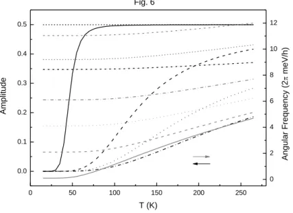
其 中 Pi 1(s2i) , Q(sg e) [(sg e)22] 及 Ne Ng LO g e E E E E ,而g及e為激子於基態與激發態時之光躍遷率,Eg及 Ee 為 激 子 之 基 態 及 激 發 態 能 量 , ENg 及 ENe 為 激 子 偶 合 光 子 與 光 聲 子 之 修 正 位 能 (normalization energies),LO為縱向光聲子之能量,0為激子與所有模態之光聲子的總 偶合強度。將(1)式及(2)式取拉氏反變換,即可得激子於基態與激發態之動態分布函 數。該分不函數除顯現激子因釋放光子所產生之衰變外,亦顯現激子與光聲子偶合後 而產生之激子-偏極子共振(既拉比震盪)。由於當激子一開始處於激發態時會自發性放 射光聲子,故激子一開始處於基態及一開始處於激發態將表現出不同的震盪頻率與振 幅,如下圖所示。 0 50 100 150 200 250 0.0 0.1 0.2 0.3 0.4 0.5 0 2 4 6 8 10 12 Amp lit u d e T (K) Fig. 6 Ang u la r F re q u e n cy (2 me V/ h )
Fig. 6. The oscillating frequency (gray) and oscillating amplitude (black) of the RO with the parameters of g 0.355eV, e 0, 0 4.6meV for =0.1meV (solid), 2.1meV (dash), 4.1meV (dot), and 6.1meV (dash-dot) with the initial conditions of Ng(0)=1 and Ne(0)=0, and for =0.1meV (short dash) and 6.1meV (short dash-dot) with
the conditions of Ng(0)=0 and Ne(0)=1. [12]
由於量子點及量子點分子中,拉比震盪之震幅及頻率與激子一開始之分布呈線性 的關係,如式(1)及式(2)所示。倘若激子分布於兩能階中,此時拉比震盪將因具有兩 種不同之共振頻率而產生互調,因此吾人將可藉由時間解析之光學量測方法量測此二 震盪頻率與振幅,在由式(1)及式(2)的關係式求出激子之分布,因而讀出量子點或量 子點分子中所儲存之資訊。此外,由於量子點分子於外加電場的作用下,可改變激子 之分布,例如電子及電洞分布於同一量子點(intra-dot exciton)或不同量子點(inter-dot exciton)。因此,吾人可利用此結果,將資訊寫入到量子點分子中,進而達到資訊寫入 的目的。 在第一年的部分計畫中,吾人將以之前所發展的理論(如上所簡述或參閱文獻[12])
為基礎,發展以量子點分子為量子位元時之資料的讀寫理論。 II. 虛擬聲子(含虛擬光聲子與虛擬聲聲子)對激子-偏極子共振之影響及其應用。 吾人在上年度的研究中,考慮量子點及量子點分子中之激子與光聲子的偶合,進 而得到拉比震盪的結果,接下來的研究中,吾人將考慮虛擬光聲子及虛擬聲聲子對拉 比震盪的影響。吾人將以下列二次量化所描述之系統的漢彌頓量為出發點,吾人亦將 沿用玻色子近似來描述激子態,
j i q j i q q i p i p pi q q q q p p p p i i i i c c d c c a d d a a E H , , , , .) . ( .) . ( 。
(3)
其中i(i)、ap(a )及p dq(dq)分別為激子、光子及聲子(含真實光聲子、虛擬光 聲子及虛擬聲聲子)之消滅(生成)算符,E 、i p及q分別為激子、光子及聲子之裸 能量。第四項為激子與光子之交互作用項,其作用強度為pi,而第五項為激子與聲子 之交互作用項,其作用強度為q。 本研究中吾人將先以標準轉換(canonical transformation),消除虛擬聲子之交作用 項,該轉換將引發不同激子態間之躍遷,激子與激子間之引力作用,及第二顆激子所 引發之不同激子態間之躍遷等。由於標準轉換後之漢米頓量變得很複雜不易處理,因 此本計劃中將仿照上年度之作法[12],先考慮三激子能階之系統,並同樣以運動方程 法(equation of motion)來求解激子之動態分布。 由於激子與光子之偶合強度遠遠小於激子與聲子之偶合強度,亦既拉比震盪之週 期遠遠小於激子因釋放光子而衰變之衰變時間,故當吾人僅關心一開始之拉比震盪行 為時,光子與激子之交互作用是可忽略的。這樣的近似下,吾人將可求得激子之動態 分布函數的解析式。從該解析式中,吾人將可探討虛擬聲子在拉比震盪中所扮演的角 色。 第二年: I. 量子點及量子點分子中激子與光聲子之偶合強度的理論計算。 在激子偏極子共振中,激子與光聲子之偶合強度是決定共振頻率、振幅及聲子作用瓶頸 (phonon bottleneck)之關鍵量。因此,第二年的部份計畫中,吾人將計算量子點及量子點分 子中,侷限性光聲子(confined optical phonon)與激子之交互作用強度。在 X.-Q. Li 等人(Phys. Rev. B59, 5069 (1999).)的研究中,假設光聲子為完美侷限於量子 點中,此時電子與侷限性光聲子之作用強度為 ) sin( ) sin( ) sin( 1 1 | | 4 0 3 q x q y q z q e z y x LO q 。 (4) 其中為立方體量子點之尺寸,及0分別為量子點材料之高頻及靜態介電常數。吾人將擴 展該理論,使其適用於激子與光聲子之交互作用強度的計算,及適用於量子點分子之交互 作用計算。
II. 多能階系統下之激子-偏極子共振行為模式之理論探討。 吾人於 2007 年所發展的理論中,是以較簡單的三激子能階模型所推演之理論,但以該 理論為背景,吾人不難想像多能階對激子衰變的貢獻。下圖所示為四能階之激子共振的示 意圖,在激發態|e1>及|e2>為弱發光態的情況下,由於圖(a)之共振路徑,將使得激子停留 於基態的機率縮短為三分之ㄧ,故最大延長衰變時間為原衰變時間之三倍,而圖(b)路徑則 使得激子停留於基態的機率僅縮短為二分之ㄧ,故最大延長衰變時間為原衰變時間之兩 倍。以此推論,可知多能階對激子衰變時間的影響甚為重要。故第二年的計劃中,吾人將 考慮多激子能階對激子-偏極子共振的影響研究。
q dark state|e1> |g> bright state |vac> pg q' |e2> dark state
q dark state|e1> |g> bright state |vac> pg q' |e2> dark state (a) (b) 吾人所用之二次量化的漢彌頓量為
j i q j i q q i p i p pi q q q LO p p p p i i i i c c d c c a d d a a E H , , .) . ( .) . ( ,
(5) 此漢彌頓量僅考慮激子與光聲子及激子與光子之交互作用,以簡化模型的複雜度。同樣的, 吾人亦將以運動方程法來求解激子之動態分布函數。在整個理論的推演中,由於多能階之 複雜度很高,求其解析解略顯困難,但於適度近似下或能獲得解析式。倘若依舊不能求得 解析解,則只能訴諸數值計算,以分析其特性。 第三年: 由於在較強的激發光源下,量子點或量子點分子中之激子數量將大於一,亦既多激子條件, 此時系統之動態特性為何,將是本年度計畫執行重點。吾人將以二次量化下之多激子系統 之漢彌頓量為出發點,如下式所示:
j i j j i i ij j i q j i q q i p i p pi q q q q p p p p i i i i V c c d c c a d d a a E H , , , , .) . ( .) . ( 。 (6) 式中除最後一項外,其餘各項則如式(3)所描述,而最後一項之位能則包含激子與激子間之 庫倫交互作用、交換交互作用(exchange interaction)及聲子所引發之交互作用,其中後二者之作用屬引力之作用,也就是具有負的偶合常數。在不考慮激子與光子及激子與聲子之交 互作用下,式(6)式是可正解的,且不會產生拉比震盪。 如前所述,由於拉比震盪之週期遠遠小於激子因釋放光子而衰變之衰變時間,故當吾 人僅關心一開始之拉比震盪行為時,將忽略光子與激子之交互作用,以簡化系統之複雜度。 即使在這樣的近似條件下,慾求激子之動態分布函數之解析式亦非易事,但如假設 Vij為常 數下,則該系統或可求得解析解。 結果與討論近代物理中,影響現代科技及生活最大的莫過於量子力學的發明,舉凡半導體的 特性、電晶體的發明、光電元件及發光體的原理等,都是拜量子力學之賜,才有今日的應用 與發展。雖然在我們的生活中,隨手捻來都是量子力學的應用,但多數人並不清楚甚麼是量子 力學,他對未來資訊科技所扮演的角色又是甚麼。在此筆者藉由本文來簡述量子力學的原理及 其於資訊科技上的應用,並簡述連結量子力學與量子資訊的關鍵元件(量子元件)之基本架構與 原理。同時亦藉由此機會,簡述筆者在近期研究中,所發現之量子元件的特有現象及其應用。 二十世紀初,物理學家從實驗的觀察中發現,物質(如電子、中子、質子等)除具有粒子的 特性外亦具有波的特性(如干涉現象),端賴於觀察者的觀測尺度而定。『遠看像朵花,近看像苦 瓜』,這句諺語正一語道破粒子與波的雙似性原理。當我們以大尺度(如微米或喱米的尺度)去觀 察物質時,就像是我們在遙遠的距離去觀察一朵花一樣,看到的只是一個大致的輪廓,甚或只 是個點狀物,而看不到花朵的結構。同樣的,以大尺度觀察電子時,我們所看到的電子就像顆 非常小的點狀粒子,而看不到波的特徵。當我們以奈米的尺度去觀察電子時,就像近看一朵花 一樣,可以清楚看到花瓣的形狀、突貣及缺陷。同樣的在奈米尺度下,我們會發現電子不像粒 子而像波,而且是『機率波』,也就是電子在時空座標中出現的機率是以波的型態出現。 因為是波,所以也就會有干涉的現象,其建設性干涉的條件,會使得電子等物質波像電磁 波一樣,產生能量量化、動量量化及角動量量化的結果,故稱之為『量子』。而破壞性干涉的結 果,將造成粒子的衰變。也因為是波,所以能像電磁波遇到介質時產生穿透與反射一樣,物質 波遇到位能障時也會有穿透及反射的現象。同樣的只要是波,就會有『測不準原理』的現象, 也就是不能同時精確測定物質波之動量與座標或時間與能量,因為動量與座標及時間與能量互 為傅立葉轉換下之對偶空間。 然而,每一種波必定存在一相對應的波動方程,1925 年薛丁格在假設卜郎克常數為一不為 零的常數下,發現只要將古典的能量方程(不考慮相對論效應下,系統之總能量等於動能加位 能,E pp 2M V(r))中之動量換成對空間座標的微分(pi , 為卜郎克常數除以 2),而將總能量換成對時間的微分(E i t),則可得到用以描述物質波的波動方程,此方 程稱之為薛丁格方程 ) ( 2 2 2 r V M t i 。 (1) 薛丁格方程的解為複數函數,稱之為波函數亦稱之為狀態向量。薛丁格方程的解有無窮多個, 每一個解均可對應到一個能量、動量甚或角動量,且各解之間彼此正交,既
i*jdvi,j,其該解可由一個或一組整數來標記之,此量化的整數即稱之為量子數。 由於解為複數函數,在真實世界中此波函數是無法直接被觀測的,但波函數的絕對值平方 (既* )則是可觀測的量,此量的意義可視為該粒子在某時空座標下出現的機率,亦可視為該粒 子的分布函數。由機率的觀點得知,只要該粒子存在於某空間中,則於整體空間中找到該粒子 的總機率必為一,既
*dv1或|1。 圖一、布拉格球[1] 近十數年來的發展中,物質的機率波特性開啟了資訊與通訊的另一個新時代『量子資訊』 與『量子通訊』。 任何具有兩個以上的離散態的系統,均可用來表示一組資訊,例如:0 與 5 伏特的電壓準位 可用來表示一個二進位數的 0 與 1,我們稱之為位元。同樣的,在量子系統中任兩個離散態(如 電子的兩個自旋態、光子的兩個極化態或原子中電子的兩離散態等),亦可用來表示一組資訊, 只是該資訊可以是任意數。舉例而言:假設有一系統具有兩個最低能量的電子態|0>及|1>,當 系統中恰有一電子時,該電子可以有一定的機率存在於這兩個態之中。換句話說,此電子的物 質波波函數或機率函數,可以是這兩個態的線性組合,既|a0 |0a1|1。其中a 及0 a 為1 複數的組合係數,以極座標來表示該系數時則為ai riexp(ii),i 為 0 或 1。以兩係數之相對相 位表示之,該電子之波函數則為|r0|0r1exp[i(10)]|1。若更進一步要求電子出現之 總 機 率 為 一 ( 既 |1 ) , 則 該 波 函 數 又 可 簡 化 為 (cos 2)|0 (sin 2)exp( )|1
| i ,其中相對相位定義為 10。此狀態向量恰為二
維之布拉格球(Bloch sphere)如圖一所示,於該球上的任一向量|>均可代表一不同資訊。此雙量 子態系統最早於 1995 年由舒馬赫所提出,並稱之為量子位元(quantum bit,簡稱 qubit)。由於和 可連續分布於 0 到 2之間,故一個量子位元可用來表示無窮多個資訊,與一個傳統的二進位位 元只能表示 0 與 1 相較,量子位元於資訊的表達上的確具有極高的效率。 傳統位元與量子位元的另一個最大不同點,就是傳統位元可以被複製,但量子位元是不可 被複製的,此特性從機率的觀點是很容易被證明的。以前述的雙量子態系統為例,所謂複製就 是必須先讀取原量子位元所儲存的資訊,再複製到另一個新的量子位元。但因量子位元中所儲 存的資訊 2 0 | | a 及 2 1 | | a ,代表著電子存在於狀態|0>及|1>的機率,這與『薛丁格的貓』的問題是
同樣的問題。一旦關貓的黑盒子被開啟,則貓是死是活立可得知,此時再談貓的死活機率則毫 無意義,此既機率的崩解。同樣的,量子位元所儲存的資訊,一旦被量測則機率分布立刻崩解, 亦既非a0 1,a1 0即a0 0,a1 1,因此原資訊是不可能被複製的。另外從波的干涉現象,亦 可證明量子資訊的不可複製性,證明細節請參閱文獻[1]本文不再贅述。此不可複製的特性,目 前已被廣泛應用於量子密碼學中,用以確保資訊的機密安全。 何謂纏縛態?想像一猜謎遊戲:有兩個紙箱各放一枚硬幣,當某甲各伸一隻手於不同的紙 箱中抓取硬幣,抓取後握拳伸出紙箱。對某乙而言,某甲左右手中各握有硬幣之機率為百分之 五十,且左右手握有硬幣之機率彼此毫無關聯,既彼此為可分離之事件。若某甲同時將雙手伸 入同一紙箱中,且其中一隻手必須握有硬幣,於抓取硬幣後同時握拳伸出紙箱。此時對某乙而 言,某甲之左右手各別握有硬幣的機率就不再是獨立的事件,其可能的狀態為|01>(既左手無硬 幣而右手則有一枚硬幣)及|10>(既左手有硬幣而右手則無),此既稱之為纏縛態。某甲的雙手可 類比為量子位元,而硬幣則可類比為電子態、電子自旋態或光子極化態等。此兩量子位元的纏 縛態亦可以貝爾(Bell states)態表式之,既 ) 10 | 01 (| 2 1 | 。 另外,亦可想像一紙箱中放有兩枚硬幣,某甲之左右手伸入該紙箱中,兩手可同時握有一枚硬 幣或同時都不握硬幣,而後握拳伸出紙箱。此時對某乙而言,某甲之左右手各別握有硬幣的機 率也不再是獨立的事件,其可能的狀態為|00>(既左右手皆無硬幣)及|11>(既左右手各 圖二、穿透式電子顯微鏡下之砷化銦/砷化鎵量子點分子結構之側面圖[2],較暗處為砷 化銦,較亮處為砷化鎵。由於砷化銦的能隙小於砷化鎵,故電子及電洞皆侷限於砷化銦 的量子點中。 有一枚硬幣),其貝爾態則為 ) 11 | 00 (| 2 1 | 。 上述之纏縛態具有非侷限性,意既一但兩量子位元形成纏縛態後,即使將兩量子位元分別 遠置兩地,其纏縛特性依舊存在,且其作用是立即的不受相對論限制的(也就是作用速度可遠遠 超越光速)。因此,若將形成纏縛態的兩量子位元分別置於甲乙兩地,藉由量子單元運算(quantum unitary operation) , 則 可 將 量 子 資 訊 藉 由 此 纏 縛 態 做 傳 遞 , 此 既 『 量 子 通 訊 』 (quantum teleportation)。量子通訊是不需物質媒介的,也不需能量轉移的,有如心靈感應般的神奇。這或 許也提供了心靈感應合理的物理解釋吧!
邏輯閘及量子資訊讀寫裝置等。所謂『量子元件』,係指以物質波的特性(如波的干涉、穿透等) 所建構的元件之統稱。然而,要表現出物質波的特性,元件的尺吋必須小於或接近物質波的波 長。由於物質波波長非常短,以電子為例:真空中的電子之波長僅不到 0.06 奈米,此時元件的 尺吋必需是原子分子的大小;而固態材料中電子的波長則為數奈米到數十奈米不等,依材料的 介電常數及材料中載子的等效質量而定,此時元件大小則為奈米尺度。 圖三、蜉蝣的腳可類比載子,水則因表面張力(類比晶格鍵結力)及蜉蝣的腳所給的壓力(類 比載子與離子間的庫倫力)而產生的形變(類比為光聲子),當載子移動時光聲子則跟著移 動。 目前量子資訊元件的研究中,有以原子分子為量子位元的,也有以半導體材料製作成量子 位元的(如量子點)。由於量子點具有與原子分子同樣的特性,因此量子點也稱之為『人造 原子』。在筆者的研究中,量子點的特性與應用,為筆者的主要研究對象。 所謂『量子點』,就是以奈米材料技術,將載子(電子或電洞)侷限於奈米尺度的空間中謂之。 由於半導體長晶及製程技術非常成熟,再加上半導體元件具有較容易整合於積體電路中的優 勢,因此由半導體材料所建構的量子位元已是目前研究的重點之ㄧ。其中砷化銦/砷化鎵量子點 及量子點分子(其結構如圖二所示),則是目前被廣泛研究的結構之ㄧ。若要以量子點做為量子 資訊元件時,必須具備載子的生命期(lifetime)及波的去相干時間(dephasing time)要高於量子運算 時間,否則運算尚未結束資訊已然消失,就如動態記憶體一樣。然而造成去相干的原因很多, 在固態材料中以原子的振動而造成載子的散射為主,此既聲子散射效應。 通常光聲子比較容易出現於離子鍵的材料中,例如 III-V 及 II-VI 族半導體。由於離子帶電, 在電場的作用下會產生晶格的形變。當帶電的載子(如電子或電洞)出現在結晶材料中時,由帶電 載子所造成的局部性電場,將使得該載子周圍的晶格變形(如圖三的類比說明)。也就是載子或光 聲子所帶的能量,可藉由庫倫力的作用而彼此相互轉移,因而產生釋放或吸收光聲子的效應。 想像當蜉蝣腳抬貣時,則水面的形變消失,此時形變位能則轉為抬腳位能,這相當於吸收光聲 子,反之則釋放光聲子。 一般認為,聲子在量子點中所扮演的角色只有負面的。然而,在筆者近期的研究中發現, 光聲子在量子點中可與帶電載子產生共振,因而提升載子的生命期,且該共振之特性亦提供量 子點中所儲存的資訊的讀寫方法。
圖四、激子-偏極子共振[12]。其中|e>代表激子之激發態,|g>代表激子之基態,|vac>代 表真空態,虛線表示光聲子的釋放與吸收,鋸齒線代表光子的釋放。 在量子點或量子點分子中,激子雖是電中性,但由於量子點結構中常存在帶電雜質、帶電缺 陷、壓電電場及內建電場,導致激子的極化而形成電偶極。此時激子可藉由此電偶極場與光聲 子產生交互作用,進而產生能量交換,既釋放或吸收光聲子。 圖五、橫座標為樣品之絕對溫度,縱座標為激子衰變時間的變化百分比。實心方塊為 InAs/GaAs 量子點分子之實驗量測結果,實心三角型為 InAs/GaAs 量子點之實驗量測結果。 變化較大之實線、虛線、點線、點虛線及雙點虛線,為激發態不發光時,且在不同的激子 -光聲子偶合強度下之理論計算結果。變化較小之實線、虛線、點線、點虛線及雙點虛線, 為激發態會發光時,在不同的激子-光聲子偶合強度下之理論計算結果[12]。 現在讓我們考慮一具有三個不同能階的激子態的系統,如圖四所示。當基態或激發態的激子 消滅時(即電子與電洞結合),激子將以釋放光子的方式釋放出能量,此結果將造成激子的衰變。 通常在量子點中,基態及激發態的激子釋放光子的機率是彼此相當的。但是在量子點分子中, 因對秤與反對秤的關係,使得激發態(又稱反對秤態)釋放光子的機率會遠小於基態(又稱對秤態)。 此外,基態的激子也可以吸收一個光聲子的方式躍遷至激發態,反之激發態的激子亦可以 釋放一個光聲子的方式回到基態。當激子重複吸收、釋放同一個光聲子的行為時,則激子可以 在 基 態 與 激 發 態 之 間 上 下 遷 移 而 形 成 共 振 現 象 , 此 既 激 子 - 偏 極 子 共 振 (excitonic-polaron resonance)。此共振的結果,將延長量子點分子中激子之生命期或衰變時間,如圖五所示,其原 理說明如下。 想像有一沙漏,漏口有一閘門,當沙漏位於激發態時漏口關閉(此類比不會發光的激子激發
q
|e> |g> |vac> pg態),反之當沙漏位於基態時漏口開啟(類比會發光之激子基態)。若沙漏一直處於基態時,其 圖六、量子點中激子之分布隨時間而變化的情形,其中實線為激發態之激子,虛線為基態 之激子。貣始條件為(a)激子一開始處於激發態,(b)激子一開始處於基態。[12] 漏沙時間假設為一個單位。則當沙漏上下遷移,且機率分佈為各百分之五十時,則總漏沙速率 將是基態與激發態速率之平均值。由於處於激發態時的沙漏不會漏沙的緣故,將使得沙漏的總 漏沙時間將延長一倍。 然而,沙漏上下遷移的機率是取決於光聲子數量的多寡,也就是溫度的高低。於絕對溫度 零度下,光聲子之數量為零,因而沒有光聲子可供激子吸收,此時激子僅能停滯於基態,故漏 沙時間為一個單位。當溫度上升時,光聲子之數量亦隨之上升,激子吸收光聲子的機率亦隨之 增加,因而增加激子於激發態的機率,而使得漏沙時間隨之延長。但由於最大分布機率為上下 各百分之五十,故最大延長時間為原來時間的兩倍。此原理可充分解釋實驗上所觀測到的現象, 如圖五所示。 若激子一開始是處於高能量的激發態,此時激子將會自發性的釋放光聲子而躍遷至基態, 再吸收該光聲子回到激發態而形成共振,如圖六所示。這種共振條件,即使溫度為絕對溫度零 度,也就是無外在因素所提供之光聲子存在,激子依然能因自發性釋放光聲子而產生共振,此 完全不同於激子一開始處於基態之共振。這兩種共振的不同處是:(1)前者頻率較低,且會隨溫 度的升高而提升。而後者頻率較高,且對溫度較不敏感。(2)前者共振振幅會隨溫度的提升而增 加,而後者則不隨溫度的變化而變化。此二不同點即可用來判斷激子的貣始狀態,進而讀出儲 存於量子點中的資訊。 由於激子與聲子具有共振的特性,吾人亦利用此特性設計一量子點系統,如圖七(a)所示。 該系統之激態與第一激發態間,可藉由激子與光子之交互作用而上下震盪,於第一激發態與第 二激發態間,則可藉由激子與光聲子之交互作用而往復震盪。此激子波函數(如下式所示)將可構 成一量子位元,並用來
圖七、(a)量子點能階示意圖;(b)量子資訊表示是意圖。[14] 代表一量子資訊。 ( ) ( )|0 ( )|1 ( )|2 | t a t bt c t 其 Rabi 軌跡則如圖八所示。 由圖中可知,該系統即使在系統溫度高達 100K 下,只要修正資訊的表示法亦能有效的運作。 該表示法由兩個基底向量來定義量子資訊,即r1T [RT(0)RT(2)] 2 與 T c T T R R r2 () , 其中 2 )] 2 ( ) 0 ( [ T T T c R R R
而RT(PA)為溫度 T 下且脈衝面積(Pulse Area)PA 下之布拉赫向量(Bloch Vector),如圖七(b)
所示。以該基底向量為基礎,則量子資訊將可表為下式 T T T r r r ()cos1 sin2 其中PA 2。在本表示法下,單一量子位元之 NOT 與 Hadamard 閘運算則可分別藉由 2-脈衝 與 /2-脈衝來達成。 目前量子計算與量子通訊之演算法已然成熟,實驗上雖然也能驗證,但只能做些簡單運算。 此外,為提高載子生命期並減少外界干擾,量子元件正常操作時的環境溫度通常在零下 260C 左右。本研究之成果,可從理論的設計、分析與驗證,說明載子之生命期與系統操作溫度之關 聯,並可藉由聲子共振來提升其生命期。此外本研究中,吾人利用單一量子點之激子與光聲子 共振之特性,設計一新的量子位元及量子資訊表示法,該量子位元於理論上證明將可操作於 100K 以下之環境溫度,此項設計十分有助於提升量子位元之操作溫度。
圖八、各種溫度下之 Rabi 軌跡。[14]
四、參考文獻
[1] Galindo and M. A. Martin-Delgado, Rev. Mod. Phys. 74, 347 (2002).
[2] W. Langbein, P. Borri, U. Woggon, V. Stavarache, D. Reuter, and A. D. Wieck, Phys. Rev. B70, 033301-1 (2004).
[3] P. Borri, W. Langbein, S. Schneider, U. Woggon, R. L. Sellin, D. Ouyang, and D. Bimberg, Phys. Rev. Lett. 87, 157401 (2001).
[4] C. Bardot, M. Schwab, M. Bayer, S. Fafard, Z. Wasilewski, and P. Hawrylak, Phys. Rev. B72, 035314-1 (2005).
[5] G. Ortner, R. Oulton, H. Kurtze, M. Schwab, D. R. Yakovlev, M. Bayer, S. Fafard, Z. Wasilewski, and P. Hawrylak, Phys. Rev. B71, 125335-1 (2005).
[6] G. J. Beirne, C. Hermannsta¨dter, L. Wang, A. Rastelli, O. G. Schmidt, and P. Michler, Phys. Rev. Lett. 96, 137401 (2006).
[7] Wen-Hao Chang, Wen-Yen Chen, Hsiang-Szu Chang, Tung-Po Hsieh, Jen-Inn Chyi, and Tzu-Min Hsu, Phys. Rev. Lett. 96, 117401 (2006).
[8] S. Strauf, K. Hennessy, M. T. Rakher, Y.-S. Choi, A. Badolato, L. C. Andreani, E. L. Hu, P. M. Petroff and D. Bouwmeester, Phys. Rev. Lett. 96, 127404 (2006).
[9] E. A. Muljarov, T. Takagahara, and R. Zimmermann, Phys. Rev. Lett. 95, 177405-1 (2005); A. Vagov, V. M. Axt, and T. Kuhn, Phys. Rev. B67, 115338 (2003); A. V. Uskov, A.-P. Jauho, B. Tromborg, J. Mork, and R. Lang, Phys. Rev. Lett. 85, 1516 (2000).
[10] P. Borri, W. Langbein, U. Woggon, V. Stavarache, D. Reuter, and A. D. Wieck, Phys. Rev. B71, 115328 (2005); M. Bayer and A. Forchel, Phys. Rev. B65, 041308 (2002).
[11] A. Vagov, V. M. Axt, T. Kuhn, W. Langbein, P. Borri, and U. Woggon, Phys. Rev. B70, 201305 (2004); A. Vagov, V. M. Axt, and T. Kuhn, Phys. Rev. B66, 165312 (2002).
[12] K.-M. Hung, J. Appl. Phys. 102, 023111 (2007).
[14] K.-M. Hung*, W.-J. Hong, K.-J. Su, T.-H. Shieh, K.-Y. Wu, and H. H. Cheng, “Temperature-dependent Rabi rotation in semiconductor quantum dots”, Appl. Phys. Lett. 96, 251903 (2010).
五、計畫成果自評
國科會補助專題研究計畫成果報告自評表
請就研究內容與原計畫相符程度、達成預期目標情況、研究成果之學術或應用價
值(簡要敘述成果所代表之意義、價值、影響或進一步發展之可能性)
、是否適
合在學術期刊發表或申請專利、主要發現或其他有關價值等,作一綜合評估。
1. 請就研究內容與原計畫相符程度、達成預期目標情況作一綜合評估
■達成目標
□ 未達成目標(請說明,以 100 字為限)
□ 實驗失敗
□ 因故實驗中斷
□ 其他原因
說明:
2. 研究成果在學術期刊發表或申請專利等情形:
論文:■已發表 □未發表之文稿 □撰寫中 □無
專利:□已獲得 □申請中 ■無
技轉:□已技轉 □洽談中 ■無
其他:
(以 100 字為限)
3. 請依學術成就、技術創新、社會影響等方面,評估研究成果之學術或應用價
值(簡要敘述成果所代表之意義、價值、影響或進一步發展之可能性)(以
500 字為限)
目前量子計算與量子通訊之演算法已然成熟,實驗上雖然也能驗證,但只能
做些簡單運算。此外,為提高載子生命期並減少外界干擾,量子元件正常操作時
的環境溫度通常在零下 260
C 左右。本研究之成果,可從理論的設計、分析與
驗證,說明載子之生命期與系統操作溫度之關聯,並可藉由聲子共振來提升其生
命期。此外本研究中,吾人利用單一量子點之激子與光聲子共振之特性,設計一
新的量子位元及量子資訊表示法,該量子位元於理論上證明將可操作於 100K 以
下之環境溫度,此項設計十分有助於提升量子位元之操作溫度。
七、 附錄
2011 出席國際會議心得報告
本年度中,計畫主持人帶領六位參與本計劃之碩士生前往中國西安出席 The International
Workshop on Physics and Mathematics (IWPM 2011)國際研討會,並發表三篇壁報論文。論文主題分別
為:(一)”VALENCE-BAND OFFSET IN ULTRA-THIN HfO2 FILM ON GaAs “;(二)”VALENCE-BAND
OFFSET IN ULTRA-THIN HfO2 FILM ON Si1-xGex/Si SUBSTRATE”;(三)” CHARGE-INDUCED
FERROMAGNETIZATION IN TWO-CARBON CLUSTERED Si”。
此次參加國際研討會收穫頗豐,除論文發表外,同時亦了解來至世界各國之專家學者的研究現況
與成果,也認識許多中國當地及其他國家之專家學者。此外,帶領學生參加本次國際會議,亦讓研究
生得以實際參與國際研討會,並認識來至世界各地的專家學者及其研究內涵,以增加國際交流與增廣
CHARGE-INDUCED FERROMAGNETIZATION IN TWO-CARBON CLUSTERED
Si
H.-C. Chang1, T.-H. Shieh2, H.-W. Ting1, K.-M. Hung1,a), J.-L. Li1 and Y.-H. Hsu1
1
Dept. of Electronics Engineering, National Kaohsiung University of Applied Sciences, Kaohsiung, Taiwan
2
Dept. of Electronics Engineering, Kun Shan University, Tainan Hsien, Taiwan
Introduction
The Si-base ferromagnetic semiconductors (FS) are of great interest as a spin-reservoir material in spintronic metal-oxide-semiconductor field-effect transistor (SMOS) and non-volatile magnetic memory (NMM) due to the convenience of the processing compatibility with modern Si fabrication technology. Even though, many diluted magnetic semiconductors, such as Co/GaAs [1], Mn/GaAs [2] and Si vacancies in SiC [3], have been proposed and widely studied, the main difficulty in realizing Si-base SMOS and NMM is still short of a suitable FS that is compatible with Si matrix. In this paper, we report a phenomenon of field-induced ferromagnetism in bulk Si with diluted two-carbon clusters (SDTC). This property not only makes the realization of Si-base SMOS possible, but also available in the applications where the field-controllable ferromagnetism is important.
Theory and Structure Model
In this work, the density functional theory (DFT) as implemented in the CASTEP and DMOL3 codes is applied to study the band structures and magnetic properties of SDTC. The DMOL3 code uses atomic-orbital basis to fully treat the interaction between core and valence electrons, while the CASTEP uses plane wave to expand the system wave functions and applies pseudo-potential approximation instead of the core states to reduce the basis and, thus, to decrease the computation. Since the DMOL3 package is more accurate in lattice constant estimation than CASTEP code, but is worse in band-gap estimation than the latter, the DOML3 code is first applied to calculate the fully relaxed structure of SDTC. This relaxed structure, then, is used to estimate the band structure and density of states using the CASTEP package with a 64-atom supercell, as shown in Fig. 1. The k-point sampling is 2x2x2 and the cutoff energy is 600eV. The interaction between core and valence electrons is included by an effective (Norm-conserving) pseudo-potential in the CASTEP package, and the generalized gradient approximation of Perdew and Wang is used for the exchange-correlation functional [4].
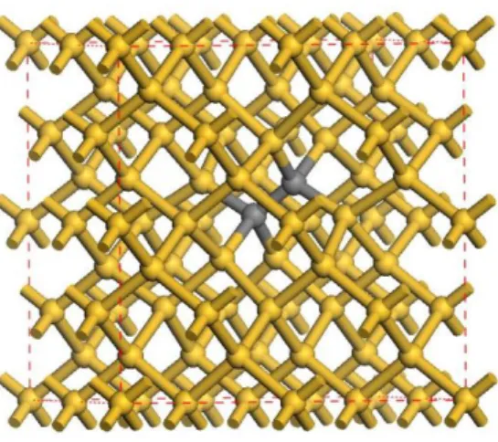
Fig. 1 A 64-atom supercell with a two-carbon cluster.
Results and Discussions
The fully-relaxed structures with (a) one electron charge (q=-1), (b) neutral charge (q=0) and (c) one hole charge (q=1) are shown in Fig. 2. The calculated results show two main features: (i) the C-C bond lengths for three different charging conditions are
the high electro-negativity of carbon atom attracts the electron from its neighbor Si atoms to the carbon site, as shown in Table-I. The additional electrons at C sites increase the Coulomb repulsive force between C atoms.
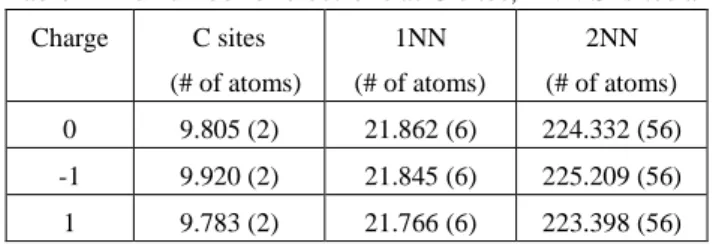
Table-I The number of electrons at C sites, 1NN Si sites and 2NN Si sites.
Charge C sites (# of atoms) 1NN (# of atoms) 2NN (# of atoms) 0 9.805 (2) 21.862 (6) 224.332 (56) -1 9.920 (2) 21.845 (6) 225.209 (56) 1 9.783 (2) 21.766 (6) 223.398 (56)
The repulsive force weakens the bond strength and pushes the carbons away from each other to elongate the bond length. For the case of q=+1, the additional hole charge mainly populates the second nearest-neighbor (2NN) Si sites that surround the C cluster. The surrounding positive charge associated with the electron charge at C sites forms an attractive force to further stretch the C-C bond length. For q=-1, a small part of the additional electron charge populates C sites and the most part populates 2NN Si sites. The increase of electron charge at C sites increases the repulsive force between C atoms, however, this force is somewhat balanced by the repulsive force according to the increased charge at 2NN Si sites. Hence, the C-C bond-length is slightly contracted in comparison with the case of q=+1.
Fig. 2 The relaxed structures of (a) q=-1, (b) q=0, and (c) q=+1, where the blue area is the net spin equi-surfaces.
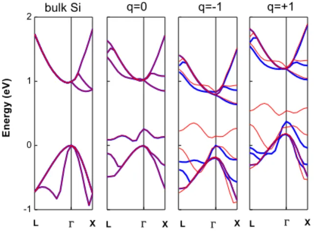
In order to understand the ferromagnetic properties of SDTC under different conditions, we calculate the band structures for bulk Si, q=0, q=-1, and q=+1 as shown in Fig. 3. The band structure of q=0 in comparison with bulk Si clearly shows an impurity band that is slightly above the valence-band maximum. A non-magnetic property is observed because the total net spin is zero as shown in Fig. 4 (black line). For q=-1, the impurity spin-up (thick-blue lines) states are occupied by additional electron charge but leaves the spin-down (thin-red lines) states empty. For q=+1, the impurity spin-up states are partially filled by the additional hole charge and the spin-down states are empty. Moreover, the spin-down heavy-hole band is lifted above the Fermi level for q=+1. The net-spin density of states as plotted in Fig. 4 exhibits a non-zero total spin in the cases of q=-1 and q=+1. The estimated total net spin is 1.297 and 1.145 for the conditions of q=+1 and q=-1, respectively. These results clearly indicate a ferromagnetic property for the cases of q=-1 and q=+1.
Conclusion
The structure of two-carbon clusters in bulk Si is studied using density functional theory. The band structure and net-spin density of states indicate that SDTC system with q=0 is non-magnetic but is ferromagnetic as the system is charging with one electron or one hole. This phenomenon can be applied to design and fabricate Si-base SMOS, NMM, and other Si-base spintronic devices where the field-controllable ferromagnetism is important.
-1 0 1 2 L X L X E n e rg y ( e V ) bulk Si q=0 q=-1 q=+1 L X L X
Fig. 3 The band structures of bulk Si and SDTC with the charges q=0, q=-1 and q=+1.
-15 -10 -5 0 5 -3 -2 -1 0 1 2 3 D ens ity of St at es (elec trons /eV) Energy (eV)
Fig. 4 The net-spin density of states for the conditions of q=0 (black line), q=-1 (red line) and q=+1 (blue line).
Acknowledgement
This work is supported by the Science Council of the Republic of China, Taiwan, under Contract No. NSC97-2112-M-151-001-MY3.
References
a) To whom all correspondence to be sent: [email protected].
[1] G. A. Prinz, Science 250, 1092 (1990); J. Islam, Y. Yamamoto, E. Shikoh, A. Fujiwara and H. Hori, Journal of Magnetism and Magnetic Materials 320, 571 (2008).
[2] S. Lee, J. H. Chung, X. Liu, J. K. Furdyna and B. J. Kirby, Materials today 12, 4 (2009); M. N. Samarth, Nature Materials 9, 955 (2010).
[3] M. Zhao, F. Pan and L. Mei, Appl. Phys. Lett. 96, 012508 (2010); F. Pan, M. Zhao and L. Mei, Appl. Phys. Lett. 108, 043917 (2010).
VALENCE-BAND OFFSET IN ULTRA-THIN HfO
2FILM ON Si
1-xGe
x/Si
SUBSTRATE
W.-C. Huang1, T.-H. Shieh2, H.-W. Ting1, K.-M. Hung1,a), J.-H. Yin 1, K.-H. Chou1 and H.-C. Chang1
1
Dept. of Electronics Engineering, National Kaohsiung University of Applied Sciences, Kaohsiung, Taiwan
2
Dept. of Electronics Engineering, Kun Shan University, Tainan Hsien, Taiwan
Introduction
Strained Si1-xGex is of great interest as one of candidate channel material in complementary metal oxide
semiconductor (CMOS) devices due to its high carrier mobility and the advantage of energy gap variation in band gap engineering associated with changing the mole fraction x of Ge atom [1]. However, there are many difficulties in realizing Si1-xGex CMOS devices according to different physical and chemical properties of Si1-xGex in comparison
with silicon. The most challenging issues that have been widely studied include the structural evolution (SE) of HfO2
during post-dielectric processes with a large thermal budget [2], the interface instability and VBO between HfO2 and
Si1-xGex [3]. However, the most studies are focused on bulk or thicker (>2nm) HfO2. The knowledge on the properties
of ultra-thin HfO2 film on Si1-xGex is poor. In this letter, the density functional theory (DFT) is applied to study the
properties of ultra-thin HfO2 film on Si1-xGex. The structural evolution of cubic-HfO2 (c-HfO2) associated with O-rich
surfaces into superstoichiometric HfOy is observed, and the variation of VBO has the range from 2.57eV to 2.82eV as
functions of Ge-atom location. Theory and Structure Model
In this work, the DFT as implemented in the CASTEP code is applied to calculate the formation energy and partial density of states (PDOS) of the structure HfO2/Si1-xGex/Si. For simplicity but without loss of generality, this study
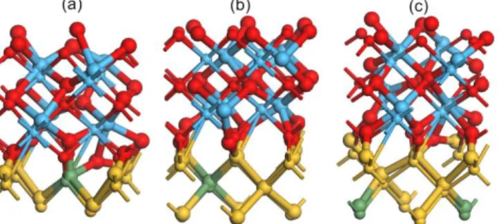
focuses on the structure of Ge mole fraction x=0.125. The interaction between core and valence electrons is included by an effective (ultra-soft) pseudo-potential. The generalized gradient approximation of Perdew and Wang [4] is used for the exchange-correlation functional. The k-mesh point is 4x4x1 and the cutoff energy for the basis functions is 300eV. The structure of HfO2/Si1-xGex/Si is modeled as a supercell which includes (i) a five-monolayer (100) Si with
fixed atomic positions, (ii) the Si layer sandwiched among two four-monolayer Si0.875Ge0.125, and (iii) a
seven-monolayer (100) c-HfO2 associated with O-rich surfaces stacked on Si0.875Ge0.125, as plotted in Fig. 1. The
modeled structures with Ge atom respectively located at the first (denoted by S1, Fig. 1(a)), second (S2, Fig. 1(b)) and
third (S3, Fig. 1(c)) layers below the HfO2 surface are applied to study SE during post-dielectric treatment with high
temperature.
Fig. 1 The relaxed (large atoms) and unrelaxed (small atoms) structures of the configurations (a) S1, (b) S2, and (c)
S3.
Results and Discussions
7-coordinated for S3, and (ii) a portion of 4-coordinated oxygen atoms relax into 2- or 3-coordinated for all
configurations. (iii) A substoichiometric SiOx is formed at the interface. Such a strongly structural deformation (iv)
causes a superstoichiometric HfOy, as shown in the figure.
The instability during structural evolution is studied by measuring the variation of formation energy. The formation energy is calculated using the equation
Si Si O O Ge Ge HfO HfO tot f E n E n E n n E E 2 2 , (1)
where Etot is the energy for the supercell containing nHfO2 bulk c-HfO2 molecules, nO excess O atoms, nGe bulk Ge
atoms, and nSi bulk Si atoms. EHfO2 is the energy per molecule of bulk c-HfO2. ESi(Ge) is the energy per atom of bulk Si
(Ge), and O is one half of O2 chemical potential.
The calculated results, as shown in Table-I, show that the Ge atom raises the formation energy as the atom moves toward the interface. In contrast, the compressive stress in Si0.875Ge0.125, as shown in Fig. 1 where the SiGe layer in S1
configuration has higher bond-length change in comparison to the others, weakens the Si-Ge bond and forces the Si atoms migrated toward the interface to release the stress. These features are well agreement with the experimental result [5], where the Ge atoms migrate toward the substrate during post-deposition annealing.
Table-I
Ef (eV) VBO (eV)
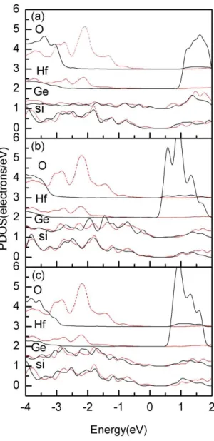
Si-HfO2 VBO(eV) SiGe-HfO2 S1 unrelaxed -7.18 0.655 0.633 Relaxed -10.62 2.13 2.57 S2 Unrelaxed -8.86 0.685 0.675 Relaxed -11.37 2.78 2.82 S3 unrelaxed -8.78 0.655 0.633 Relaxed -12.46 2.24 2.68
The VBO of the structure is directly measured from PDOS [6]. The figure 2 shows the calculated PDOS for the centered Si, Si0.875Ge0.125 and HfOy layers. The valence band maximum (VBM) of HfOy is the average of Hf and O
layers. The VBO between different materials is read to be the difference of the corresponding VBMs. The results for S1, S2 and S3 configurations with/without relaxation are shown in Table-I. As seen from the table, the VBO is
significantly affected by structural relaxation and charge redistribution. The strain-induced bond breaking in hafnia layer gives rise to a superstoichiometric HfOy with y=2.06 for S1, y=2.125 for S2, and y=2.111 for S3. The excess
oxygen in hafnia layer attracts the valence electrons in Si0.875Ge0.125/Si substrate into oxygen sites due to high oxygen
electro-negativity. The effect of charge redistribution results in a dipole around the interface, increases potential difference between hafnia and Si0.875Ge0.125/Si layers, and, thus, increases VBO in comparison with unrelaxed
structure. Conclusions
The VBO of ultra-thin c-HfO2 film on Si0.875Ge0.125/Si substrate is studied using DFT theory. The heavy stress in hafnia
layer significantly causes the structure deformation and results in a superstoichiometric HfOy. The calculated
formation energy shows that the Ge atom more farther from the interface is more stable, which is well agreement with experiment. The excess O atom in HfOy redistributes the charge density and increases its VBO. This effect should be
Fig. 2 The PDOS of (a) S1, (b) S2 and (c) S3 with (solid lines) and without (dashed lines) relaxations.
Acknowledgement
This work is supported by the Science Council of the Republic of China, Taiwan, under Contract No.
NSC97-2112-M-151-001-MY3.
References
b) To whom all correspondence to be sent: [email protected]. [1] T. J. Park, et al., J. Appl. Phys. 92, 232906 (2008).
[2] M.H. Cho et al., Appl. Phys. Lett. 84, 1171 (2004). [3] Jiyoung Jang et al., Appl. Phys. Lett. 92, 232906 (2008). [4] J. P. Perdew and Wang Yue, Phys. Rev. B, 33, 8800 (1986).
[5] T. J. Park, et al., Electrochemical and Solid-State Letters 10, G97 (2007). [6] P.W. Peacock and J. Robertson, Phys. Rev. Lett 10, 1103 (2004).
VALENCE-BAND OFFSET IN ULTRA-THIN HfO
2FILM ON GaAs
Z.-W. Hsue1, T.-H. Shieh2, H.-W. Ting1, K.-M. Hung1,a) and B.-Y. Hou1, J.-L. Li1, C.-H. Nin1, Y.-C. Tsai1
1
Dept. of Electronics Engineering, National Kaohsiung University of Applied Sciences, Kaohsiung, Taiwan
2
Dept. of Electronics Engineering, Kun Shan University, Tainan Hsien, Taiwan
Introduction
GaAs is of great interest as one of candidate channel material in complementary metal oxide semiconductor (CMOS) devices due to its high electron and hole mobility [1]. There are many difficulties in realizing GaAs CMOS devices according to different physical and chemical properties of GaAs in comparison with Si. The most challenging issues that have been widely studied include the structural evolution (SE) of HfO2 during
post-dielectric processes with a large thermal budget [2], the interface instability and valence band offset (VBO) between HfO2 and GaAs [3], especially, for the HfO2 film being smaller than 2nm, which has been widely used
in modern CMOS technology with the channel length smaller than 45nm [4]. However, the most studies are focused on the film greater than 2nm. The knowledge on the properties of ultra-thin HfO2 film on GaAs is poor.
In this letter, the density functional theory (DFT) is applied to study the properties of ultra-thin HfO2 film on
GaAs. The oxygen-rich cubic-HfO2 (c-HfO2) and monoclinic-HfO2 (m-HfO2) are studied. The partial density of
states (PDOS) and valence band offset (VBO) are calculated. Theory and Structure Model
In this work, the DFT as implemented in the CASTEP code is applied to calculate the formation energy, partial density of states (PDOS) and VBO of ultra-thin HfO2 film on GaAs. The interaction between core and valence
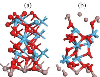
electrons is included by an effective (ultra-soft) pseudo-potential. The generalized gradient approximation of Perdew and Wang [5] is used for the exchange-correlation functional. A Monkhorst-Pack k-point sampling mesh 4x4x1 is used, and the cutoff energy for the basis functions is 300eV. The structure of HfO2/GaAs is modeled as
a supercell which includes (i) a fifteen-monolayer (100) GaAs with fixed atomic positions and with Ga rich surfaces, (ii) a seven-monolayer (100) c(m)-HfO2 with O-rich surfaces being stacked on the GaAs, as plotted in
Fig. 1(a) (Fig. 1(b)).
The fully-relaxed structure (large atoms) shows that the hafnia layer is strongly deformed to relax the highly tensile strain that is forced by GaAs substrate according to a large lattice mismatch. The dilation of hafnia layer breaks a part of Hf-O bonds to absorb the stress, and results in: (i) the 8-coordinated Hf atom in c-HfO2
collapses into 6-coordinated, and the 7-coordinated Hf atoms in m-HfO2 collapse into 5-, 6- and 7-coordinated;
(ii) the 4-coordinated O atoms in c-HfO2 relax into 3-coordinated, and the 3- and 4-coordinated O atoms in
m-HfO2 relax into 2-, 3- and 4-coordinated. (iii) Since the lattice constants of m-HfO2 (a=5.18 Å, b=5.185 Å and
c=5.284 Å) is more close to GaAs (5.65 Å) than c-HfO2 (5.115 Å), the structure deformation of m-HfO2 is
weaker than c-HfO2 as shown in Fig. 1. Such a weaker deformation in m-HfO2, however, results in a
superstoichiometric HfOy (y=2.2), but the stronger deformation in c-HfOy retains y=2. In addition, the m-HfO2
has different surfaces along (100) and (100), where a two-oxygen surface presents in (100) plane but a three-oxygen surface in (100) plane.
Fig. 1 The relaxed (large atoms) and unrelaxed (small atoms) structures of (a) c-HfO2/GaAs and (b)
m-HfO2/GaAs.
Results and Discussions
The structure instability during structural evolution is studied by measuring the variation of formation energy. The formation energy is calculated using the equation
As As O O GaAs GaAs HfO HfO tot f E n E n E n n E E 2 2 , (1)
where Etot is the energy for the supercell containing nHfO2 bulk c-HfO2 molecules, nO excess O atoms, nGaAs bulk
GaAs molecules, and nAs bulk As atoms. EHfO2 is the energy per molecule of bulk c-HfO2. EGaAs is the energy per
molecule of bulk GaAs, EAs is the energy per atom of bulk As, and O is one half of O2 chemical potential.
The calculated results, as shown in Table-I, show that the c-HfO2 is more stable than m-HfOy.
Table-I
Ef (eV) VBO (eV)
c-HfO2 unrelaxed -1.0971 2.2125 relaxed -11.446 1.2175 m-HfO2 unrelaxed 3.2097 0.7576 relaxed -3.0927 1.8894
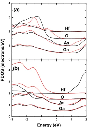
The VBO of the structure is directly measured from PDOS [6]. In Figure 2, the calculated PDOSs for the centered GaAs and HfO2 layers are plotted. The valence band maximum (VBM) of GaAs is the average of Ga
-3 -2 -1 0 1 2 0 1 2 3 4 0 1 2 3 4 -3 -2 -1 0 1 2 0 1 2 3 4 0 1 2 3 4 P D O S ( e le c tr o n s /e V ) Energy (eV) (b) Hf Ga As Ga O O Hf (a) As
Fig. 2 The PDOS of (a) c-HfO2/GaAs and (b) m-HfO2/GaAs with (black lines) and without (red lines)
relaxations.
The VBO is read to be the difference of VBMs of GaAs and HfO2. The calculated results for c-HfO2/GaAs and
m-HfO2/GaAs with/without relaxation, as shown in Table-I, indicate that the VBO is significantly affected by
structural relaxation. The strain-induced bond breaking in hafnia layer gives rise to an additional charge transfer between HfO2 and GaAs, and results in VBO variation. For c-HfO2, the VBO decreases after relaxation
according to the charge transfer from c-HfO2 to GaAs, contrarily, increases for m-HfO2 due to a backward
charge transfer from GaAs. The backward charge transfer is mainly resulted from the excess O atoms in superstoichiometric HfOy, because the large electro-negativity of O atom attracts the valence electrons in GaAs
into O sites. Conclusions
The VBO of ultra-thin c-HfO2 and m-HfO2 films on GaAs substrate is studied using DFT theory. The heavy
stress in hafnia layer significantly causes the structure deformation and results in a charge transfer and superstoichiometric m-HfOy. The calculated formation energy shows that the c-HfO2 is more stable than
m-HfO2, which is well agreement with experiment. The VBO of the structure c-HfO2/GaAs is increased, while
that of m-HfO2/GaAs is decreased after structure relaxation, according to the charge transfer between HfO2 and
GaAs. These characteristics of ultra-thin HfO2 film should be observed in CMOS devices made from an
ultra-thin HfO2 dielectric film stacked on GaAs channel.
Acknowledgement
References
a) To whom all correspondence to be sent: [email protected]. [1] T.J.Park et al., J. Appl. Phys. 92, 232906 (2008).
[2] Weichao Wang, et al., Applied Surface Science 256, 6569 (2010).
[3] Weichao Wang et al, J. Appl. Phys. 114, 22610 (2010).
[4] Intel, Meet the world’s first 45 nm processor, see for example, http://www.intel.com/technology/
silicon/45nm_technology.htm (January 2006).
[5] J. P. Perdew and Wang Yue, Phys. Rev. B, 33, 8800 (1986).
國科會補助計畫衍生研發成果推廣資料表
日期:2011/08/28國科會補助計畫
計畫名稱: InAs/GaAs量子點及量子點分子中之激子衰變與拉比震盪研究 計畫主持人: 洪冠明 計畫編號: 97-2112-M-151-001-MY3 學門領域: 半導體物理-理論無研發成果推廣資料
97 年度專題研究計畫研究成果彙整表
計畫主持人:洪冠明 計畫編號:97-2112-M-151-001-MY3 計畫名稱:InAs/GaAs 量子點及量子點分子中之激子衰變與拉比震盪研究 量化 成果項目 實際已達成 數(被接受 或已發表) 預期總達成 數(含實際已 達成數) 本計畫實 際貢獻百 分比 單位 備 註 ( 質 化 說 明:如 數 個 計 畫 共 同 成 果、成 果 列 為 該 期 刊 之 封 面 故 事 ... 等) 期刊論文 0 0 100% 研究報告/技術報告 0 0 100% 研討會論文 0 0 100% 篇 論文著作 專書 0 0 100% 申請中件數 0 0 100% 專利 已獲得件數 0 0 100% 件 件數 0 0 100% 件 技術移轉 權利金 0 0 100% 千元 碩士生 6 0 100% 博士生 0 0 100% 博士後研究員 0 0 100% 國內 參與計畫人力 (本國籍) 專任助理 0 0 100% 人次 期刊論文 3 0 100% 其中 Appl. Phys. Lett. 96, 251903 (2010)論文,亦獲 選為 2010 年七月 所發行之 Virtual Journal of Nanoscale Science and Technology 的 文 章。 研究報告/技術報告 0 0 100% 研討會論文 7 0 100% 篇 論文著作 專書 0 0 100% 章/本 申請中件數 0 0 100% 專利 已獲得件數 0 0 100% 件 件數 0 0 100% 件 技術移轉 權利金 0 0 100% 千元 碩士生 6 0 100% 博士生 0 0 100% 博士後研究員 0 0 100% 國外 參與計畫人力 (外國籍) 人次其他成果