Nanogap Structure Optimization and Electron Emission Study
of the Surface Conduction Electron Emitter Fabricated
by Palladium Hydrogenation
Chih-Hao Tsai and Fu-Ming PanzDepartment of Materials Science and Engineering, National Chiao-Tung University, Hsinchu, 30050 Taiwan
High-pressure Pd hydrogenation was used to fabricate a single nanogap on the Pd strip electrode of the surface-conduction electron emitter共SCE兲. The large stress induced by the Pd hydrogenation resulted in formation of a nanogap in the Pd electrode at the step area over the Pt/Ti contact pad in the SCE structure. The gap width was a function of not only Pd hydrogenation conditions but also the dimension of the SCE structure. Finite element analysis was used to study the stress distribution in the SCE structure with the Pt/Ti contact pad of various thicknesses so that an SCE structure with a minimized gap width could be obtained. Among the SCE emitters under study, the optimal SCE structure, which was with a Pt/Ti contact pad thickness of 20 nm and had a Pd nanogap width of 18 nm, exhibited the best field-emission performance. Compared to the conventional SCE emitter with a planar nanogap, the hydrogenated SCE emitter demonstrated a much higher emission efficiency 共⬃4%兲. The better electron emission performance of the hydrogenated SCE emitter was ascribed to so that the emitter cathode had a rugged and protruding edge structure.
© 2009 The Electrochemical Society. 关DOI: 10.1149/1.3083231兴 All rights reserved.
Manuscript submitted December 1, 2008; revised manuscript received January 16, 2009. Published February 26, 2009.
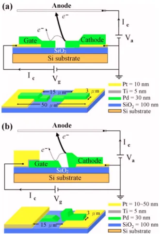
When the prototype of the surface-conduction electron-emitter display共SED兲, which is one kind of flat-panel display 共FPD兲 based on a field-emission mechanism, was brought to the public by Canon cooperation, it immediately attracted wide attention.1-5 SED has many performance advantages over many other FPDs, such as better brightness, lower power consumption, and faster response time. The electron field-emission device of the Canon SED, surface-conduction electron共SCE兲 emitter, has a nanosized gap ⬃4 to 6 nm wide with a planar sidewall structure, where electron field emission takes place. Figure1a schematically shows the conventional SCE emitter structure. Although the Canon SED offers many perfor-mance advantages over most commercially available FPDs, the fab-rication process of the SED is complicated and expensive. One of the difficult fabrication steps is to fabricate the matrix array of SCE emitters in which the nanogap was produced on the palladium oxide line electrode via a series of tedious electrical forming and activa-tion processes. Moreover, the SED has a very low electron emission efficiency共⬍1 to 3%兲, which is an important parameter for display performance, such as power consumption and luminous efficiency. In a previous study, we developed a simple method to fabricate nanogaps on a Pd line electrode by high-pressure hydrogenation.6 The mechanistic principle of the Pd nanogap fabrication is based on the well-known phenomenon that hydrogenation of a Pd thin film may lead to hydride formation and concurrent phase transformation, which is accompanied by the buildup of a large compressive stress in the Pd film due to a large volume increase共12%兲.7By appropri-ately controlling hydrogenation parameters, we have successfully fabricated a nanogap 25 nm wide on the Pd line electrode at room temperature. The nanogap had a protruding cathode structure with an inclining sidewall as schematically shown in Fig. 1b. Electron trajectory simulations using the three-dimensional 共3D兲 finite-difference time-domain particle-in-cell method showed that the pro-truding nanogap structure provided better emission efficiency and focusing capability in comparison to the conventional SCE emitter with the planar nanogap.8 In this work, we further optimized the SCE structure to minimize the nanogap separation with the assis-tance of finite element analysis of the hydrostatic stress distribution in the SCE structure, and the electron emission property of the hy-drogenated SCE emitter was studied.
Experimental
The detailed fabrication process of the hydrogenated SCE emitter can be found in the previous report.6In brief, as illustrated in Fig.
1b, the Pd nanogap SCE emitter was fabricated on a p-type 共100兲 silicon wafer. The Si wafer was first thermally oxidized to form a SiO2 insulator layer 150 nm thick. Liftoff photolithography was used to pattern the SCE structure. Before the Pd line electrode was patterned, a Pt/Ti contact pad having a width of 30 m and various
zE-mail: [email protected]
Figure 1.共Color online兲 Schematic diagrams of the two-dimensional and 3D
configuration of共a兲 the conventional SCE and 共b兲 the hydrogenated SCE structures. Electron emission trajectories from the cathode toward the anode 共thick arrow兲 and the gate electrode 共dashed line兲 are also illustrated. The thickness of each component thin film in the SCE structures is given by the color bars.
thicknesses was deposited on the SiO2layer. A Pd strip 30 nm thick, 3m wide, and 50 m long was deposited on the wafer with one end overlapping the Pt/Ti contact pad and the rest deposited on the SiO2 layer. Deposition of the Pd, Ti, and Pt thin films were all performed by electron-beam evaporation deposition. Hydrogenation of the Pd/Pt/Ti stacked structure was then performed at 25°C at a pressure of⬃2 ⫻ 104mbar for 30 min to develop a nanogap on the Pd strip at the step between the Pt/Ti contact pad and the SiO2layer. After the Pd hydrogenation, the pressure was evacuated to 0.3 mbar for 30 min at 330°C for hydrogen desorption. After the nanogap formation, a Pt共50 nm兲/Ti共5 nm兲 contact pad was deposited at the end of the gate side of the ruptured Pd strip to complete the prepa-ration of the SCE emitter structure. Electrical properties of the SCE emitters, such as the conduction current共Ic兲 and the emission cur-rent共Ie兲, were measured at room temperature under a vacuum con-dition of⬍5 ⫻ 10−6Torr using a Keithley 237 measurement sys-tem and a power source syssys-tem 共Matsusada Precision Inc., AU-10R6兲. The anode was a mechanically polished stainless steel plate with a mirrorlike surface and was placed 550m above the SCE emitter array. For comparison, a planar nanogap 25 nm in gap width was also prepared at the middle on a Pd strip in the SCE structure similar to that shown in Fig.1aby a focused ion beam共FIB兲 system 共FEI Company兲 using the gallium ion source at a beam energy of 30 keV. The width and length of the Pd strip and the underlying Pt/Ti contact pads of the FIB-prepared SCE emitter were the same as those of the hydrogenated SCE emitters. The thickness of the Pd strip and the Pt/Ti pad were 30 and 15 nm, respectively. The tailed preparation process of the FIB-cut nanogap has been de-scribed in a previous report.9
Results and Discussion
On the basis of previous model studies, the electron emission efficiency of an SED display, which decides the luminous perfor-mance of the FPD, is closely related to the nanogap separation and the geometric shape of the nanogap structure.8,10,11 Although the nanogap separation determines the turn-on voltage of the SCE emit-ter according to the Fowler–Nordheim共F-N兲 theory, the geometric shape of the nanogap structure can significantly modify the electric field distribution on the SCE emitter, thereby affecting the electron emission behavior. Therefore, optimization of the electron emission efficiency of an SED display can be achieved by minimizing the nanogap separation and fabricating a suitable nanogap structure, al-lowing effective electron emission toward the screen anode.
Optimization of the SCE emitter structure.— According to hy-drostatic stress distribution study by finite element analysis, the film stress resulting from Pd volume expansion due to hydrogenation is highly concentrated near the step between the Pt/Ti contact pad and the SiO2substrate, and the magnitude of the stress accumulation is strongly dependent on the height of the Pt/Ti pad. To optimize the SCE structure, we prepared four separate SCE structures with the Pt/Ti contact pads of various total thicknesses 共10, 15, 20, and 25 nm兲, in which the Ti layer had a fixed thickness of 5 nm. In the following discussion, we will refer to these SCE structures as SCE-10, SCE-15, SCE-20, and SCE-25 nm, where the number in the abbreviations denotes the thickness of the Pt/Ti contact pad. After hydrogenation at 25°C at a pressure of⬃2 ⫻ 104mbar for 30 min, one single nanogap was successfully produced on the Pd strip both in the SCE-15 and SCE-20 nm structures. Cracking also occurred in the Pd strip in the SCE-10 and SCE-25 nm structures, but the crack did not fully develop into a complete nanogap across the Pd strip 共i.e., the regions around the two sides of the step were not broken兲. Figure 2a-c shows the plane-view scanning electron microscope 共SEM兲 images of the nanogaps developed separately in SCE-15, SCE-20, and SCE-25 nm structures, respectively. In order to show the incomplete rupture in the SCE-25 nm structure, the SEM image of Fig.2chas a smaller magnification than the SEM images of Fig.
2aand b. The nanogaps developed in the SCE-15 and SCE-20 nm structures had a gap separation of 25 and 18 nm, respectively. The
nanogap separation was evaluated by averaging the measured dis-tances across the nanogap in ten different regions in the plain-view SEM images of Fig.2. For the SCE-25 nm structure, as shown in Fig. 2c, a discontinuous crevice but not a through nanogap was formed in the Pd strip at the corner area of the middle section of the step. The cross-sectional SEM images of the SCE-15, SCE-20, and SCE-25 nm structures are also shown in Fig.2d-f. One edge of the nanogap exhibited a rugged and protruding feature. According to Fig.2f, some thin connections between the two sides of the crack in the SCE-25 nm structure can be clearly seen.
Finite element analysis was performed to study the hydrostatic stress distribution in the SCE structure after the high-pressure hy-drogenation. The finite element analysis showed that, after the vol-ume expansion due to Pd hydrogenation, the Pd film strip in the SCE-20 nm structure had the largest stress developed around the step. Figure3shows the cross-sectional and 3D maps of the hydro-static stress distribution in the SCE-15, SCE-20, and SCE-25 nm structures. Parameters required for the finite element analysis, such as the thermal expansion coefficient, elastic modulus, and Poisson ratio of the constituent materials, have been reported elsewhere.6,12 According to Fig.3a-c, the SCE structure had a large stress buildup around the step corner of the hydrogenated Pd strip overlying on the Pt/Ti contact pad. It can be clearly seen from Fig. 3b for the SCE-20 nm structure that the stress induced by the Pd hydrogena-tion was heavily distributed diagonally in the region across the step corner of the Pd strip, as indicated by the dashed open circle, to the step edge of the Pt/Ti contact pad. The top area near the step edge of the Pd strip exhibited much less stressed as marked by the square. Figure 2. The plane-view and cross-sectional SEM images of nanogaps
developed separately in different SCE structures by hydrogenation treatment at 25°C:共a兲 and 共d兲 for SCE-15 nm, 共b兲 and 共e兲 for SCE-20 nm, and 共c兲 and 共f兲 for SCE-25 nm structures. Note that the image magnification in 共c兲 is smaller than共a兲 and 共b兲 for better view of the crevice at the step in the SCE-25 nm structure. The cross-sectional SEM specimens were prepared by etching out a deep crater in the SCE structure using a FIB.
Pd atoms in the highly stressed region at the step bottom would diffuse toward the top area near the step edge, where it was the least stressed as compared to another area around the step.6As a result, a rugged protrusion structure could be formed on the cathode side as the nanogap developed in the Pd strip via stress-induced atom mi-gration. The protruding sidewall on the cathode of the hydrogenated SCE structure can be clearly observed in the cross-sectional SEM images of Fig.2d-f. The rugged protruding sidewall of the cathode can greatly enhance the emission efficiency of the SCE emitter as will be discussed later.
Although the SCE-15 nm structure had a smaller stress accumu-lation at the step, it had a wider nanogap separation than the SCE-20 nm structure. We believe that a joint dynamical behavior of stress relaxation and stress-induced atom migration during Pd hy-drogenation determines the observed gap separation. Once a nan-ogap is fully developed along the step, the stress is rapidly relieved in the area adjacent to the nanogap and atom diffusion from the gap edges toward the longitudinal direction will eventually stop, thereby preventing the nanogap from growing wider. The much larger stress strength developed in the SCE-20 nm structure would result in a faster nanogap formation and could thus lead to a narrower nanogap separation as compared to the SCE-15 nm structure. The 3D stress distribution maps of Fig.3may provide a more explicit illustration on the stress distribution along the step across the 3m wide Pd strip and give a better understanding of how the accumulated stress relaxes. For the SCE-20 nm structure, the stress is largely concen-trated along the step bottom, apparently extends to the two side ends of the step, and the area near the top edge of the step is the least stressed. Compared to the SCE-20 and SCE-15 nm structures, the SCE-25 nm structure was the least stressed in the step region. Be-cause the SCE-20 nm structure has stress distribution more concen-trated both in the longitudinal and lateral directions near the step region of the hydrogenated Pd strip, a complete nanogap can rapidly
develop along the step via atomic diffusion driven by the stress gradient. When the stress accumulation is less concentrated at the step, the stress can be relaxed more evenly in all directions in the narrow Pd strip electrode, and thus a thorough crack along the step cannot be readily achieved. For the SCE-25 nm structure, both the cross-sectional and 3D stress distribution maps show a less drastic change in the stress distribution along the step as compared to the SCE-15 and SCE-20 nm structures, suggesting that an effective stress-induced cracking is more difficult to take place. This could explain the observation in the SEM image of Fig.2cthat a crevice but not a through nanogap was formed on the Pd strip in the SCE-25 nm structure.
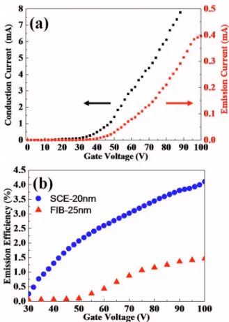
Emission characteristics of the SCE emitter.— On the basis of the F-N theory, an electron field emitter with a smaller distance between the cathode and the anode can exhibit better field emission characteristics in terms of the current density and the turn on volt-age. Therefore, the SCE with the 18 nm nanogap is certainly ex-pected to have a better field emission performance than the one with the 25 nm nanogap. Figure 4a shows the field emission current 共hereafter will be referred to conduction current, Ic兲 as a function of the applied voltage between the cathode and the gate electrodes 共gate voltage, Vg兲 of the SCE-20 and SCE-15 nm emitters. It can be clearly seen that the SCE emitter with the 18 nm nanogap 共SCE-20 nm兲 had a larger conduction current than the one with the 25 nm nanogap共SCE-15 nm兲 at the same gate voltage. A very high conduction current of 1.5 mA was measured for the 18 nm nanogap at the gate voltage of 50 V. Figure 4b is the F-N plot of the SCE-20 nm emitter, which shows a linear feature in the high gate voltage regime, indicating that the electron conduction in the nan-ogap followed the F-N field emission mechanism. The turn-on volt-age, which is defined herein as the gate voltage at which the curve of the F-N plot begins to exhibit linear rising feature, is ⬃30 and Figure 3. 共Color online兲 The
cross-sectional and 3D maps of the hydrostatic stress distribution in the hydrogenated SCE structures: 共a兲 and 共d兲 SCE-15 m emitter, 共b兲 and 共e兲 SCE-20 nm emitter, and共c兲 and 共f兲 SCE-25 nm emitter. In Fig.
3b, the area marked by the dashed circle is with the maximal stress and by the square the least stressed.
⬃41 V for the SCE-20 and SCE-15 nm emitters, respectively. Also shown in Fig.4ais the current-voltage共I-V兲 curve of an SCE emit-ter with a planar nanogap structure similar to that of the conven-tional SCE structure schematically shown in Fig. 1a. The planar nanogap was 25 nm in gap width and prepared by etching a Pd strip using a FIB instead of Pd hydrogenation and will be referred to as FIB-25 nm hereafter. Unlike the hydrogenated SCE emitters, the FIB-25 nm emitter had a flat cathode surface with smooth gap edges.9Compared to the hydrogenated SCE-15 nm emitter, the FIB-prepared SCE had a smaller Ic with a larger turn-on voltage 共⬃50 V兲. According to previous model studies, a tilting and pro-truding cathode structure of the nanogap emitter can yield a better electron field emission efficiency due to the highly concentrated electric field at the cathode edge.8,10Thus, the better field emission characteristics of the hydrogenated SCE can be ascribed to the pro-truding cathode structure and a rugged cathode edge, both of which can effectively enhance the local electric field around the cathode, thereby improving the field emission performance.
The majority of electrons field emitted from the cathode flows into the gate electrode, converting into the conduction current共Ic兲, whereas some electrons field emitted from the gap-edge side of the cathode can be extracted to the screen anode, becoming the emission current共Ie兲 as shown in Fig.1a. Because Icis much larger than Ie, the electron emission efficiency 共兲 of the SED display, which is defined as = Ie/Ic, is generally very low共⬍3%兲.5Figure5ashows the plots of Icand Ieas a function of the gate voltage共Vg兲 under a fixed anode voltage of 1.1 kV for the SCE-20 nm emitter. Also shown in Fig.5bis the plot for against Vg. It should be noted that no emission current could be measured before the conduction cur-rent began to flow in the SCE emitter共i.e., before field emission took place in the nanogap兲. This indicates that electrons emitted
toward the screen anode are not due to the diode-type field emission between the screen anode and the cathode of the SCE emitter. Both Ic and Ie increased with the gate voltage, and exhibited an asymptotic increase against the gate voltage. An value as high as ⬃4% can be achieved at a gate voltage of 100 V. The SCE-15 nm emitter had a similar trend of variation in Icand Ieagainst Vgas the SCE-20 nm emitter共not shown兲, and the value nearly the same as that of the SCE-20 nm emitter over the gate voltage range under study. The asymptotic increase of the value with the gate voltage indicated that Ieis not a simple linear proportional function of Ic. The emission efficiency of the FIB-25 nm emitter is also shown in Fig. 5b, and a much smaller value 共⬃1.03%兲 was measured at Vg= 100 V. In addition to the gate voltage, is also greatly depen-dent on the anode voltage共Va兲. The values of the 20, SCE-15, and FIB-25 nm emitters as a function of the anode voltage are shown in Fig.6. To measure the-Vacurves, we kept the Icat 1 mA for all three emitters and Vawas varied from 0 to 1.1 kV. Like the -Vgcurve, the-Va plot also showed an asymptotic increase fea-ture. As can be seen from Fig.6, the values of the SCE-20 and SCE-15 nm emitters are almost the same, and much larger than that of the FIB-25 nm emitter. This suggests that the geometric shape of the cathode is a characteristic factor determining the electron emis-sion efficiency of an SCE emitter.
According to model studies of the electric field distribution, cou-pling of the gate and the anode voltages will create two electric field distribution zones around the conventional nanogap SCE emitter.13 The inner zone determines how field-emitted electrons travel on the SCE surface and the outer zone decides the emission electron tra-jectory toward the screen anode from the SCE emitter. Asai et al.12 Figure 4.共Color online兲 共a兲 The conduction current 共Ic兲 as a function of the
gate voltage共Vg兲 of 共1兲 SCE-20 nm, 共2兲 SCE-15 nm, and 共3兲 FIB-25 nm emitters.共b兲 The F-N plot of the SCE-20 nm emitter.
Figure 5. 共Color online兲 共a兲 Plots of the conduction current 共Ic兲 and the
emission current共Ie兲 as a function of the gate voltage 共Vg兲 under a fixed anode voltage of 1.1 kV for the SCE-20 nm emitter.共b兲 The emission effi-ciency共兲 against Vgof the SCE-20 nm and the FIB-25 nm emitters. The SCE-15 nm emitter had a similar-Vg curve feature as the SCE-20 nm emitter.
proposed that electrons emitted from the cathode may reach the gate surface near the nanogap edge, as shown by the dotted line in Fig.1, in compliance with the downward field developed on the gate elec-trode, and subsequently undergo multiple elastic scattering on the gate surface before they are finally attracted toward the anode.13 Kim et al.13and Lo et al.,14taking inertial force and Lorentz force, respectively, into account, have demonstrated by electron trajectory simulation that those electrons attracted to the anode screen are mostly emitted directly from the top surface area near the cathode edge. Changes in the gate and anode voltage can significantly alter the electric field distribution around the nanogap region, thereby varying the emission current density and the electron trajectory from the emitter toward the screen anode. This is particularly true for the hydrogenated SCE emitter, of which the cathode has a tilting pro-trusion structure. Compared to a planar nanogap structure of the conventional SCE emitter, a less symmetric electric field distribution can be developed across the nanogap in the hydrogenated SCE emit-ter, and the electric field strength is much higher around the tip corner of the protruding cathode.10,11 The much higher emission efficiency for the SCE-15 and SCE-20 nm emitters than for the FIB-25 nm emitters suggests that the protruding cathode structure with a rugged morphology plays the major role in improving the electron emission performance.
Conclusion
We have fabricated the Pd nanogap in the SCE emitter by prop-erly controlling the location and strength of the compressive stress developed in a Pd strip electrode during the high-pressure Pd hydro-genation. We used finite element analysis to study hydrostatic stress distribution in the SCE structure and optimized the SCE structure by tuning the thickness of the Pt/Ti contact pad. The stress distribution
analysis showed that the SCE structure with a Pt/Ti contact pad of 20 nm in thickness had the most concentrated stress developed in the Pd strip at the step of the Pt/Ti contact pad. The optimal SCE structure had a Pd nanogap 18 nm in width and demonstrated the best field emission performance among all the SCE structures under study in terms of the field emission current and the turn-on voltage. Compared to the conventional SCE emitter with a planar nanogap structure, the hydrogenated SCE emitter had better field emission properties and a higher emission efficiency. An emission efficiency as high as 4% was obtained at the gate voltage of 100 V for hydro-genated SCE emitters, which was about four times the emission efficiency of the FIB-prepared SCE emitter. The much better elec-tron emission characteristics of the hydrogenated SCE emitter can be ascribed to the tilting protruding structure and the rugged mor-phology of the nanogap on the cathode side. The study demonstrates that the Pd hydrogenation is an ideal method to fabricate Pd nan-ogaps in SCE emitters for SED applications.
Acknowledgments
This work was supported by the National Science Council of Taiwan under contract no. NSC96-2221-E009109-MY3 and by Chunghwa Picture Tubes, Ltd., Taiwan. Technical support from Na-tional Nano Device Laboratories is gratefully acknowledged. We thank Professor Yiming Li of National Chiao Tung University for the discussion about electron emission simulation for the SCE emit-ter.
National Chiao Tung University assisted in meeting the publication costs of this article.
References
1. M. I. Elinson, A. G. Zhdan, G. A. Kudintseva, and M. E. Chugunova, Radio Eng.
Electron. Phys., 10, 1290共1965兲.
2. I. Nomura, K. Sakai, E. Yamaguchi, M. Yamanobe, S. Ikeda, T. Hara, K. Hatanaka, and Y. Osada, in Proc. IDW’96, p. 523共1996兲.
3. K. Sakai, I. Nomura, E. Yamaguchi, M. Yamanobe, S. Ikeda, T. Hara, K. Hatanaka, Y. Osada, H. Yamamoto, and T. Nakagiri, in Proc. EuroDisplay’96, p. 569共1996兲. 4. E. Yamaguchi, K. Sakai, I. Nomura, T. Ono, M. Yamanobe, N. Abe, and T. Hara, J.
Soc. Inf. Disp., 5, 345共1997兲.
5. K. Yamamoto, I. Nomura, K. Yamazaki, S. Uzawa, and K. Hatanaka, SID Int.
Symp. Digest Tech. Papers, 36, 1933共2005兲.
6. C. H. Tsai, K. J. Chen, F. M. Pan, M. Liu, and C. N. Mo, Appl. Phys. Lett., 90, 163115共2007兲.
7. F. A. Lewis, The Palladium/Hydrogen System, pp. 13–49, 94–117, Academic Press, London共1967兲.
8. Y. Li and H. Y. Lo, J. Phys. D, 41, 085301共2008兲.
9. C. H. Tsai, K. J. Chen, F. M. Pan, H. Y. Lo, Y. Li, M. C. Chiang, and C. N. Mo, J.
Electrochem. Soc., 155, J361共2008兲.
10. W. Benenson, J. W. Harris, H. Stocker, and H. Lutz, Handbook of Physics, pp. 239–240, Springer, New York共2002兲.
11. H. Y. Lo, Y. Li, H. Y. Chao, C. H. Tsai, and F. M. Pan, Nanotechnology, 18, 475708共2007兲.
12. A. Asai, M. Okuda, S. Matsutani, K. Shinjo, N. Nakamura, K. Hatanaka, Y. Osada, and T. Nakagiri, SID Int. Symp. Digest Tech. Papers, 10, 127共1997兲.
13. Y. S. Kim, Y. G. Kim, D. I. Kim, J. G. Kang, S. O. Kang, E. H. Choi, and G. Cho,
Jpn. J. Appl. Phys., Part 2, 39, L684共2000兲.
14. H. Y. Lo, Y. Li, C. H. Tsai, H. Y. Chao, and F. M. Pan, IEEE Trans. Nanotechnol.,
7, 434共2008兲. Figure 6. 共Color online兲 Plots of the emission efficiency 共兲 values as a
function of the anode voltage共Va兲 for 共a兲 SCE-20 nm, 共b兲 SCE-15 nm, and 共c兲 FIB-25 nm emitters.