New Transient Detection Circuit for System-Level ESD Protection
Cheng-Cheng Yen, Chi-Sheng Liao, and Ming-Dou Ker Nanoelectronics and Gigascale Systems Laboratory
Institute of Electronics, National Chiao-Tung University, Hsinchu, Taiwan
A
BSTRACTA new on-chip transient detection circuit for system-level electrostatic discharge (ESD) protection is proposed. By including this new proposed on-chip transient detection circuit, a hardware/firmware solution cooperated with power-on reset circuit can be co-designed to fix the system-level ESD issues. The circuit performance to detect different positive and negative ESD-induced fast electrical transients has been investigated by HSPICE simulator and verified in silicon chip. The experimental results in a 0.18-Pm CMOS process have confirmed that the proposed on-chip transient detection circuit can detect fast electrical transients during system-level ESD zapping.
I
NTRODUCTIONSystem-level ESD issue is an increasingly significant reliability issue in CMOS IC products [1]. This tendency results from the strict requirements of reliability test standards, such as system-level ESD test for electromagnetic compatibility (EMC) regulation [2]. In the system-level ESD test standard of IEC 61000-4-2, the electrical/electronic product must sustain the ESD level of +8kV (+15kV) under contact-discharge (air-discharge) test mode to achieve the immunity requirement of “level 4.” Such high-energy ESD-induced noises often cause damage or malfunction of CMOS ICs inside the equipment under test (EUT). It has been found that some CMOS ICs are very susceptible to system-level ESD stress, even though they have passed the component-level ESD specifications such as human-body-model (HBM) of r2kV, machine-model (MM) of r200V, and charged-device-model (CDM) ofr1kV [3].
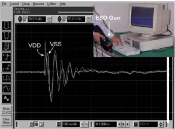
The inset figure in Figure 1 shows an EUT (keyboard) which is stressed by an ESD gun with charged voltage of +1kV zapping on the horizontal coupling plane (HCP). During the system-level ESD test, the power and ground lines of the microcontroller IC no longer maintain their normal voltage levels, but an underdamped sinusoidal voltage with the amplitude of several hundred volts instead, as shown in Figure 1. Such a high-voltage-level fast transient causes the keyboard to be upset or frozen after the system-level ESD zapping.
In order to meet the system-level ESD specifications, two useful methods have been reported [4], [5]. One effective method is to add some discrete noise-decoupling components or board-level noise filters into the CMOS IC products to decouple, bypass, or absorb the electrical transient voltage (energy) under system-level ESD test, such as capacitor filters, ferrite bead, or, transient voltage suppressor (TVS) [4]. The other method to improve the system-level ESD immunity of CMOS ICs is to regularly check the system abnormal conditions by using an external hardware timer, such as a retriggerable monostable multivibrator [5]. However, the additional discrete noise-bypassing components increase the total cost of microelectronics system. Therefore, an integrated on-chip solution in standard CMOS processes without adding additional discrete noise-decoupling components on the printed circuit board is strongly requested by IC industry [6].
Figure 1. Measured VDD and VSS waveforms of the microcontroller
ICs inside the keyboard with ESD voltage of +1kV zapping on the HCP under system-level ESD test.
In this paper, a new on-chip transient detection circuit is proposed to detect the fast electrical transients under the system-level ESD tests. The new proposed transient detection circuit can be combined with the power-on reset circuit to provide a hardware/firmware system co-design for system-level ESD solution. The performance of new proposed on-chip transient detection circuit to sense different fast electrical transients has been investigated by HSPICE and verified in silicon chip. The transient-induced latchup (TLU) measurement method and the system-level ESD gun are both used to evaluate the detection function of the proposed on-chip transient detection circuit [7]. The experimental results in a 0.18-Pm CMOS process have verified that the proposed on-chip transient detection circuit can successfully detect fast electrical transients during system-level ESD zapping.
T
RANSIENTD
ETECTIONC
IRCUITA. Circuit Structure
Figure 2 shows the proposed on-chip transient detection circuit. The RC-based circuit structure is designed to realize the transient detection function. The PMOS device (Mp1) is designed to help to
memorize the logic state before and after system-level ESD stresses. The NMOS device (Mnr) is used to provide the initial reset function
to set the initial voltage level on node VA and the initial output
voltage (VOUT) level to 0V. In Figure 2, the node VX is biased at VDD
during the normal power supply operation condition. Under the system-level ESD stress, the ESD voltage has fast rise time in the order of nanosecond (ns). The voltage level of VX has much slower
voltage response than the voltage level at VDD because the RC
circuit is designed to have a time constant in the order of microsecond (Ps). Due to the longer delay of the voltage increase at the node VX, the PMOS device (Mp1) can be turned on by the
overshooting ESD voltage and conducts a voltage to node VA. The
turned-on Mp1 device can pull up the voltage level at node VA.
Therefore, the logic level stored in the node VA is changed to detect
the system-level ESD event. The output voltage of the proposed on-chip transient detection circuit is finally changed from 0V to 1.8V to memorize the occurrence of system-level ESD events.
Figure 2. The new proposed on-chip transient detection circuit.
B. Simulation
The simulation tool (HSPICE) is used to investigate the on-chip detection circuit performance under the system-level ESD test. In simulation, the underdamped sinusoidal waveforms are used to simulate fast electrical transients on the power lines of the proposed on-chip transient detection circuit under system-level ESD tests.
The simulated VDD, VSS, and VOUTwaveforms of the proposed
on-chip transient detection circuit with a positive-going underdamped sinusoidal voltage on both VDD and VSS are shown in
Figure 3. The positive-going underdamped sinusoidal voltage with amplitude of +4V is used to simulate the positive ESD stress under the system-level ESD test. Under ESD stress, VDD(VSS) begins to
increase rapidly from 1.8V (0V). VOUTis disturbed simultaneously
during VDD and VSS disturbance. During this period, the proposed
on-chip transient detection circuit can detect the occurrence of disturbance on VDD and VSS. As a result, after VDDfinally returns to
its normal voltage level of 1.8V, VOUT will be changed from 0V to
1.8V.
The simulated VDD, VSS, and VOUTwaveforms of the proposed
on-chip transient detection circuit with a negative-going underdamped sinusoidal voltage on both VDD and VSS are shown in
Figure 4. The negative-going underdamped sinusoidal voltage with amplitude of -4V is used to simulate the negative ESD stress under the system-level ESD test. The VOUT is influenced by the VDD and
VSS disturbance through the coupling paths. Finally, the output
(VOUT) of the transient detection circuit is changed from 0V to 1.8V.
Figure 3. Simulated VDD, VSS, , and VOUT waveforms of the
proposed transient detection circuit with positive-going underdamped sinusoidal voltage on both VDDand VSS.
Figure 4. Simulated VDD, VSS, and VOUT waveforms of the
proposed transient detection circuit with negative-going underdamped sinusoidal voltage on both VDD and VSS.
By using HSPICE, the capability of the proposed transient detection circuit to sense fast electrical transients has been analyzed. From the simulations, the output voltage of the proposed transient detection circuit can be changed and kept at stable voltage level of 1.8V after system-level ESD events. The HSPICE simulation can be used to design the device sizes in the proposed on-chip transient detection circuit to detect fast electrical transients.
T
RANSIENT-I
NDUCEDL
ATCHUP(TLU) T
ESTA. Measurement Setup
With the system-level ESD test, it can only judge whether the EUT passes the required criterion through its abnormal function (e.g. EUT shuts down). Nevertheless, it is hard to directly evaluate the system-level ESD immunity of a single IC inside the EUT. To solve this problem, a component-level TLU measurement setup with the following two advantages is used [8]. First, the transient-induced latchup (TLU) immunity of a single IC can be evaluated by the measured voltage and current waveforms through oscilloscope. Second, with the ability of generating an underdamped sinusoidal voltage, how an IC inside the EUT is disturbed by the ESD-generated noise under the system-level ESD test can be accurately simulated. Figure 5 depicts such a component-level TLU measurement setup. An electrostatic-discharge simulator is used as the TLU-triggering source, VCharge, to produce an underdamped
sinusoidal voltage stimulus. Through applying a positive (negative) charged voltage (VCharge), the intended positive-going
(negative-going) underdamped sinusoidal voltage can be generated as the voltages generated from ESD gun under the system-level ESD test.
In the measurement setup shown in Figure 5, a charging capacitance of 200pF is used to store charges offered by the TLU-triggering source, VCharge, and then these stored charges are
discharged to the device under test (DUT) through the relay. The intended underdamped sinusoidal voltage can be produced to simulate the transient voltage on the power pins of CMOS ICs under the system-level ESD test, no matter which polarity (positive or negative) the ESD voltage is. Moreover, a small current-limiting resistance (5:) is recommended to protect the DUT from electrical-over-stress (EOS) damage during a high-current (low-impedance) latchup state.
Figure 5. Measurement setup for transient-induced latchup (TLU).
B. Measurement Results
The proposed on-chip transient detection circuit has been fabricated in a 0.18-Pm CMOS process. With the TLU measurement setup in Figure 5, the VDD and VOUT transient responses can be
recorded by the oscilloscope.
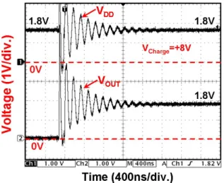
Figs. 6 and 7 show the measured VDD and VOUT transient
responses of the proposed on-chip transient detection circuit under the stress with VCharge of +8V and -1V, respectively. As shown in
Figure 6, under the stress with VCharge of +8V, VDD begins to
increase rapidly from 1.8V. VOUT is disturbed simultaneously with
positive underdamped sinusoidal voltage on VDD power line. After
the TLU test with an initial VCharge of +8V, the output (VOUT) of the
transient detection circuit is changed from 0V to 1.8V. As shown in Figure 7, under the stress with VCharge of -1V, VDD begins to
decrease rapidly from 1.8V. VOUTis disturbed simultaneously with
negative underdamped sinusoidal voltage on VDD power line. After
the TLU test with an initial VCharge of -1V, the output voltage (VOUT)
of the proposed on-chip transient detection circuit is significantly increasesd from 0V to a stable voltage of 1.8V.
From the TLU test results, the proposed on-chip transient detection circuit can successfully detect fast electrical transients on VDD power line. With positive and negative underdamped sinusoidal
voltages on VDD power line, the output voltages (VOUT) of the
proposed on-chip transient detection circuit are changed from 0V to a stable voltage of 1.8V.
Figure 6. Measured VDD and VOUT transient responses on the
proposed on-chip transient detection circuit under TLU test with VCharge of +8V.
Figure 7. Measured VDD and VOUT transient responses on the
proposed on-chip transient detection circuit under TLU test with VCharge of -1V.
S
YSTEM-L
EVELESD T
ESTA. Measurement Setup
In the test standard of IEC 61000-4-2 [2], two test modes have been specified: air-discharge test mode and contact-discharge test mode. Figure 8 shows the measurement setup of the system-level ESD test with indirect contact-discharge test mode, which consists of a wooden table on the ground reference plane (GRP). In addition, an isolation plane is used to isolate the EUT from horizontal coupling plane (HCP). The HCP are connected to the GRP with two 470k: resistors in series.
By using the digital oscilloscope, the transient responses on power lines of CMOS IC products can be recorded and analyzed. Before each ESD zapping, the initial output voltage (VOUT) of the
proposed transient detection circuit is measured to make sure the correct output voltage of 0V. After each ESD zapping, the VOUT
voltage is measured to check the final voltage level in order to verify the detection function. Thus, the circuit performance of the proposed transient detection circuit can be evaluated with this measurement setup.
Figure 8. Measurement setup of the system-level ESD test with indirect contact-discharge test mode. The ESD gun zapping on the horizontal coupling plane (HCP) could cause underdamped sinusoidal voltage waveform on the power lines of CMOS ICs inside the EUT.
B. Measurement Results
The system-level ESD test with indirect contact-discharge test mode is used to experimentally verify the proposed transient detection circuit. With both positive and negative fast electrical transients, the VDD transient response can be recorded by the
oscilloscope. This can clearly indicate whether the detection circuit works correctly during the system-level test. With the system-level ESD tests, the measured waveforms can be compared with the simulated waveforms.
The measured VDDand VOUT waveforms of the proposed on-chip
transient detection circuit with ESD voltage of +0.2kV zapping on the HCP under system-level ESD test are shown in Figure 9. VDD
begins to increase rapidly from the normal voltage (+1.8V). Meanwhile, VOUT begins to greatly increase due to such a
high-energy ESD stress. During the period with disturbance on VDD, VOUT
is disturbed simultaneously. Finally, the output voltage (VOUT) of the
transient detection circuit is changed from 0V to 1.8V. As a result, the proposed on-chip transient detection circuit can memorize the occurrence of the system-level ESD stress. The experimental result in Figure 9 is consistent with the HSPICE simulation results in Figure 3.
The measured VDD and VOUT transient waveforms of the
proposed transient detection circuit with ESD voltage of -0.2kV zapping on the HCP under system-level ESD test are shown in Figure 10. During VDD disturbance, VOUT is disturbed
simultaneously. Obviously, VOUT is finally pulled up to 1.8V after
the system-level ESD test. The experimental result in Figure 10 is consistent with the HSPICE simulation results in Figure 4.
The detection capability of the proposed on-chip transient detection circuit under the system-level ESD test has been proven by both the experimental results in silicon chip and the HSPICE simulation. From the experimental results, the proposed on-chip transient detection circuit can indeed detect and memorize the occurrence of system-level ESD stress. For microelectronic products, the detection results from the proposed on-chip transient detection circuit can be used as a system recover signal for firmware check. When the fast electrical transient happens, the on-chip transient detection circuit can detect the fast electrical transients and change the output state (VOUT) from 0V to 1.8V. Then, the firmware can
execute the recover procedure to recover all system functions after system-level ESD stress.
Figure 9. Measured VDDand VOUT transient responses with ESD
voltage of +0.2kV zapping on the HCP under system-level ESD test.
Figure 10. Measured VDDand VOUT transient responses with ESD
voltage of -0.2kV zapping on the HCP under system-level ESD test.
C
ONCLUSIONA new on-chip transient detection circuit for system-level ESD protection has been proposed and implemented in a 0.18-Pm CMOS process. The detection capability under different positive and negative fast electrical transients has been also investigated by HSPICE. The experimental results have verified that the proposed on-chip transient detection circuit can detect fast electrical transients due to system-level ESD zapping. The proposed on-chip transient detection circuit can be combined with the firmware design and power-on reset circuit to provide an effective solution to solve the system-level ESD issue in CMOS IC products.
R
EFERENCES[1] M.-D. Ker and S.-F. Hsu, “Physical mechanism and device simulation on transient-induced latchup in CMOS ICs under system-level ESD test,” IEEE Trans. Electron Devices, vol. 52, no. 8, pp. 1821–1831, Aug. 2005.
[2] IEC 61000-4-2 Standard, “EMC – Part 4-2: Testing and
measurement techniques – Electrostatic discharge immunity test,” IEC, 2001.
[3] M.-D. Ker and Y.-Y. Sung, “Hardware/firmware co-design in a 8-bits microcontroller to solve the system-level ESD issue on keyboard,” in Proc. EOS/ESD Symp., 1999, pp. 352–360.
[4] M.-D. Ker and S.-F. Hsu, “Evaluation on board-level noise filter networks to suppress transient-induced latchup in CMOS ICs under system-level ESD test,” IEEE Trans.
Electromagnetic Compatibility, vol. 48, no. 1, pp. 161–171,
Feb. 2006.
[5] M. I. Montrose, Printed Circuit Board Design Techniques for
EMC Compliance, IEEE Press, 2000.
[6] M.-D. Ker, C.-C. Yen, and P.-C. Shin, “On-chip transient detection circuit for system-level ESD protection in CMOS ICs,” in Proc. IEEE Custom Integrated Circuits Conference, 2006, pp. 361–364.
[7] M.-D. Ker and S.-F. Hsu, “Component-level measurement for transient-induced latchup in CMOS ICs under system-level ESD considerations,” IEEE Trans. Devices Mater. Reliab., vol. 6, no. 3, pp. 461–472, Sep. 2006.
[8] M. Kelly, L. Henry, J. Barth, G. Weiss, M. Chaine, H. Gieser, D. Bonfert, T. Meuse, V. Gross, C. Hatchard, and I. Morgan, “Developing a transient induced latch-up standard for testing integrated circuits,” in Proc. EOS/ESD Symp., 1999, pp. 178– 189.