國 立 交 通 大 學
電子工程學系 電子研究所碩士班
碩 士 論 文
具有奈米線通道的多晶矽薄膜電晶體之特性改善
Performance Enhancement in
Thin-Film-Transistors with Poly-Si Nanowire
Channels
研 究 生:蔡銑泓
指導教授:林鴻志 博士
黃調元 博士
具有奈米線通道的多晶矽薄膜電晶體之特性改善
Performance Enhancement in Thin-Film-Transistors with Poly-Si
Nanowire Channels
研 究 生:蔡銑泓 Student:Hsien-Hung Tsai
指導教授:林鴻志 博士 Advisor:Dr. Horng-Chin Lin
黃調元 博士 Advisor:Dr. Tiao-Yuan Huang
國 立 交 通 大 學
電子工程學系 電子研究所碩士班
碩 士 論 文
A Thesis
Submitted to Department of Electronics Engineering & Institute of Electronics College of Electrical and Computer Engineering
National Chiao Tung University in partial Fulfillment of the Requirements
for the Degree of Master in
Electronics Engineering June 2006
具有奈米線通道的多晶矽薄膜電晶體之特性改善
研究生:蔡銑泓
指導教授:林鴻志 博士
黃調元 博士
國立交通大學
電子工程學系 電子研究所
摘 要
在本論文中,我們研製一種新型奈米線薄膜電晶體,並使用兩種方法來
降低在該新型奈米線薄膜電晶體的漏電流。第一種方法是在頂部的閘極
與汲極交疊區域中,閘極與氧化層之間,加入一層額外的氮化矽,藉此
降低閘極/氧化層交界處的電場強度,以有效減少閘引致汲極漏電流
(GIDL)漏電流。第二種方法則是加入快速升溫退火製程來改善晶體的特
性,藉此降低缺陷對漏電流的貢獻。由研究中結果來看,兩種方法均為
有效。
此外,針對奈米線通道品質的改進,我們也使用金屬誘導側向結晶
(MILC)的方式來加以改善,並藉此大幅提昇奈米線薄膜電晶體的特性。
由電子顯微鏡分析的結果發現,沿著電晶體通道方向有大的針狀形的晶
體結構,使得通道有類似單晶體的結構與特性,因此元件的電特性包含
載子遷移率、次臨界擺幅等可得到明顯的改善。此外,在本研究中也比
較了不同位置的成核開口配置對元件特性的影響。
Performance Enhancement in Thin-Film-Transistors with Poly-Si
Nanowire Channels
Student: Hsien-Hung Tsai Adviser: Dr. Horng-Chih Lin
Dr. Tiao-Yuan Huang
Department of Electronics Engineering & Institute of Electronics
National Chiao Tung University
Abstract
In this study, a novel nanowire (NW) transistor was fabricated and characterized. Two methods were explored to reduce leakage current of the newly-proposed nanowire
devices. One is to insert a Si3N4 layer in between the gate oxide and gate in the top
gate-to-drain overlap region to effectively reduce the strength of electrical field and thus the magnitude of the gate-induced drain leakage (GIDL). The other scheme is to apply an additional RTA step to improve the film quality. Both methods are shown to be effective in this regard.
MILC method was also employed to improve the channel film crystallinity and the characteristics of NW-TFTs. Transmission electron microscopy (TEM) characterization indicates that the needle-like grain with crystallization direction along the NW channel is
resulted, and leads to a single-crystal-like structure as the lateral size of the grain approach to the NW dimensions. Electrical characteristics including carrier mobility and subthreshold swing were dramatically improved with this approach. The impact of seeding window arrangements were also explored in this study.
誌 謝
在這篇論文完成的同時,首先我要感謝我的指導老師黃調元老師及林鴻志老 師,黃調元老師即使生病了,仍然不遺餘力的引導我,使我在半導體的領域可以一 步步的前行;而林鴻志老師以身作則,鍛練出我正確的研究方式以及獨力思考、分析 的能力。我真的相當感謝兩位老師無私的指導,讓我在兩年來收穫很多也能夠在此 時順利將論文完成。 再來,我要感謝帶著我做實驗、量測、分析的蘇俊榮學長,學長對求知的積極 以及做研究的嚴謹態度都深深地使我受到影響。此外,盧文泰學長、李耀仁學長、 葉冠麟學長、呂嘉裕學長、李明賢學長、林宏年學長、盧景森學長、張尹鋒學長、 房新原學長、林賢達學長、李聰杰學長、藍文廷學長,這兩年來很感謝你們對我的 幫助。 接著我要感謝在實驗室一起努力的好夥伴,黃健銘、趙志誠、洪振家、謝雨霖、 徐行徽、張凱翔、呂建松還有雖然不是我們實驗室但常常來我們實驗室一起努力的 沈香谷。這兩年因為大家互相幫忙,使我在遇到問題不怕無法解決,在做研究總能 達到事半功倍的效果;也因為大家,我很喜歡去實驗室,實驗室不只是一個做研究的 好地方,也是一個充滿了我溫馨回憶的地方。 我要感謝和我一起在交大的大學同學,張家源、溫思凱、蔣宗翰、賴宏斌、唐 仕豪、蔡宗翰、李佳蓉、林晏慶以及孫汝玉,因為你們的扶持,讓我在進入陌生的 交大時,不會感到無助。 最後我要感謝我的父母以及家人,很感謝我的父母在這二十多年來對我的栽培 以及我家人對我的支持,使我在求學的時候沒有後顧之憂。 要感謝的人太多,還有許多是上述所沒提到的,在此致上最誠摰的歉意及無限 的謝意。再次感謝所有的陪我一路走來的人,謝謝。Contents
Abstract (in Chinese) ...i
Abstract (in English)...iii
Acknowledgement (in Chinese)... v
Contents ...vi
Table Captions ...viii
Figure Captions...ix
Chapter 1 Introduction... 1
1.1 Overview of polycrystalline silicon thin film transistors... 1
1.2 Overview of nanowires ... 2
1.3 Metal induced lateral crystallization of amorphous silicon ... 3
1.4 Thesis organization ... 5
Chapter 2 Device Fabrication and Measurement ...6
2.1 Device structure and process flow ... 6
2.2 Electrical characterization and measurement setup ... 8
Chapter 3 Leakage current reduction in NW-TFTs ...10
3.1 Leakage mechanisms ...10
3.1.1 Leakage mechanisms in channel region... 10
3.1.2 Leakage current mechanism in gate-to-drain overlap
region... 11
3.2 Effects of Si
3N
4hard mask layer ...12
3.3 Effects of NH
3plasma hydrogenation...15
Chapter 4 NW-TFTs fabricated by MILC ...17
4.1 Electrical characteristics of NW-TFTs fabricated by MILC ...17
4.2 Analysis for NW-TFTs with different MILC seeding window
arrangement ...18
Chapter 5 Conclusions...21
References...22
Table Captions
Table 3-1. Electrical characteristics of as-fabricated device and devices
which received 2-hr and 3-hr NH
3plasma treatment. ...28
Table 4-1. Comparisons of device parameters between n-type SPC and
MILC NW-TFTs. ...29
Table 4-2. Comparisons of device parameters between p-type SPC and
Figure Captions
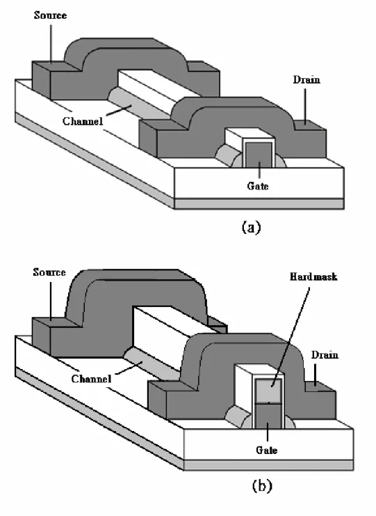
Fig. 2-1. Schematics of (a) control NW-TFT (b) NW-TFT with hard mask.
...31
Fig. 2-2. Top view of NW-TFT...32
Fig. 2-3. The definition of the poly-Si nanowire channel. ...32
Fig. 2-4. SEM picture of a device fabricated by SPC. ... 33
Fig. 3-1. Leakage mechanisms in channel. (a) Thermionic emission. (b)
Thermioic field emission. (c) Band-to-band tunneling...34
Fig. 3-2. Band diagram illustrating GIDL occurrence. ... 35
Fig. 3-3. Schematic layout illustrating the gate-to-drain overlap region.
...36
Fig. 3-4. Transfer characteristics of NW-TFTs with HM, both with and
without plasma treatment...37
Fig. 3-5. Leakage currents of NW TFTs with HM having various gate
widths. ...38
Fig. 3-6. (a) comparison of leakage currents of NW TFTs with and w/o
HM having various gate widths, (b) comparison of the normalized
off-state current for devices with and w/o HM as a function of gate
width. |V
GD| = 10 V...39
Fig. 3-7. Transfer characteristics
of NW-TFT with HM at various
temperatures...40
Fig. 3-8. Off-state activation energies of NW-TFTs with and without HM.
...41
Fig. 3-9. Energy band diagram in gate-to-drain overlap region for
NW-TFTs with HM. ...42
Fig. 3-10. TEM of NW-TFT with HM. ...43
Fig. 3-11. Transfer characteristics of as-fabricated device and devices
which received 2-hr and 3-hr NH
3plasma treatment at (a) V
D=0.5V,
(b) V
D=3V... 44
Fig. 3-12. Transfer characteristics of control NW-TFTs. ...45
Fig. 3-13. Off-state I
D-V
Gcharacteristics of NW-TFTs after 2hr-NH
3plama treatment. ...46
Fig. 3-14. Off-state currents of control NW-TFTs (w/o Si
3N
4mark mask)
having various gate widths. ...47
Fig. 3-15. (a) comparison of leakage currents of NW TFTs with and w/o
RTA having various gate widths, (b) comparison of the normalized
off-state current for devices with and w/o RTA as a function of gate
width. |V
GD| = 10 V...48
Fig. 3-16. Off-state activation energies of NW-TFTs with and without
RTA. ...49
Fig. 4-1. Crystallization mechanism of MILC. The arrows represent the
crystallization direction. ...50
Fig. 4-2. The plane-view TEM of MILC NW-TFT. ...51
Fig. 4-3. Comparison of transfer characteristics between n-type MILC
and SPC NW-TFTs. ...52
Fig. 4-4. Comparison of transfer characteristics between n-type MILC
Fig. 4-5. Comparison of transfer characteristics between p-type MILC
and SPC NW-TFTs ...54
Fig. 4-6. Configurations of MILC seeding window. (a) Asymmetric
seeding window (at source). (b) Asymmetric seeding window (at
drain). (c) symmetric seeding window. ...55
Fig. 4-7. I
D-V
Gcharacteristics of devices fabricated by asymmetric MILC
seeding window...56
Fig. 4-8. I
D-V
Gcharacteristics of RTA devices fabricated by asymmetric
MILC seeding window. ...57
Fig. 4-9. Comparison of I
D-V
Gcharacteristics between devices fabricated
Chapter 1
Introduction
1.1
Overview of polycrystalline silicon thin film
transistors
Thin film transistors (TFTs), which employ a thin semiconductor film on an insulating substrate as the active device channel, were first demonstrated in 1961 by Dr.
Weimer of RCA [1-3]. In 1966, the first polycrystalline silicon TFT (poly-Si TFT) was
fabricated by Fa et al. [4]. Since then, conduction mechanism, fabrication process and electrical properties of polycrystalline silicon films were extensively studied [5] [6]. Compared with amorphous silicon TFTs (α-Si TFTs), poly-Si TFTs have many advantages, such as superior carrier mobility, CMOS capability, and better device reliability [7]. The growth of interest in poly-Si TFTs has been stimulated by the rapid commercial development of active matrix-addressed flat-panel liquid-crystal displays
(AMLCDs)and high performance EEPROMs [8-10].
Poly-Si material consists of silicon crystallites (grains). Between them, there are regions with high density of impurities, called grain boundaries. The detrimental effects of grain boundaries and in-grain defects on the poly-Si TFT performance have been investigated and are well recognized [11] [12]. The performance degradation of the devices arises from the presence of a high density of trapping states at the grain boundaries. Therefore the crystallization methods that govern the number and size of
grains are very important. Up to date, there are mainly several crystallization methods employed to transfer α-Si into poly-Si, including solid phase crystallization (SPC) [13], metal induced crystallization (MIC) [14] and excimer laser crystallization (ELC) [15]. Besides, it is well known that hydrogen passivation eliminates these traps and improves the performance of poly-Si TFTs [16] [17]. The effect of hydrogen passivation on trap states has been characterized by using field-effect analysis on poly-Si TFTs [18], and the correlations between trap-state density reduction and hydrogen diffusivity in a TFT structure have been reported.
Although poly-Si TFTs with relatively high on/off current ratio have been fabricated, their leakage current still imposes a severe limit on the duration of video information that
can remain on a pixel before it needs to be refreshed.Some mechanisms for the leakage
current of TFTs have been investigated, and two major mechanisms were proposed [19]
[20]. One is related to the thermal emission while the other involves the band-to-band tunneling process. Furthermore, specific device structure may be susceptible to specific leakage current, such as GIDL-like leakage generated at the gate to drain overlap region [21]. Generally, the leakage current is strongly dependent on the number of defects presenting in poly-Si channel. Measuring the off-state current and estimating the associated activation energy are useful to identify the dominant mechanism.
1.2
Overview of nanowires
Minimization of silicon electronics is being actively pursued. One-dimensional structures, such as nanowires (NWs), have great potential for testing and understanding
fundamental concepts about the role of dimensionality and size in electrical properties, and could be the ideal building block for nanoelectronics because they can function both as the devices and interconnect wires that access them. Owing to the inherent high surface-to-volume ratio feature, NWs can suppress short-channel effects encountered in nano-scale MOSFETs [22] and provide high surface sensitivity for sensing devices. Many possible applications of Si NWs have been exploited, including nano CMOS, memory devices [23], NW TFTs [24], and biosensors [25]. The preparation of Si NWs could be categorized into two types, namely, top-down [23] and bottom-up [24][25]. Methods used to assemble and align the NWs prepared by “bottom-up” approach include electric-field-directed assembly [26], microfluidic channel [27] and Langmuir-Blodgett
(LB) technique[28]. Electric field method is to arrange NWs by means of the interactive
electric field between two parallel electrodes and the polarity of NWs. Although electric fields enable more control over assembly, this method is limited by electrostatic interference between nearby electrodes and requirement of extensive lithography to fabricate the electrodes. Microfluidic channel method is to align wires by flowing NWs suspension inside a poly (dimethylsiloxane) (PDMS) mold, and could obtain layer-by-layer assembly of multiple crossed NW arrays. However, the size of fluidic channels may limit alignment of NWs. LB method could assemble a large-area
anisotropic NWs by a compression process, but it is restricted to preparation of one
monolayer. Overall, for practical applications, more refinement is needed to improve the reproducibility and controllability of the above methods.
amorphous silicon
Metal induced crystallization (MIC) of amorphous silicon, amorphous germanium, or amorphous SiGe has been intensely investigated with either double layers of metal and the amorphous semiconducting material [29-31] or metal implanted into Si or Ge [32] [33]. Studies showed that MIC could dramatically decrease the temperature necessary for the crystallization of a-Si and a-Ge. For those metals forming eutectics with Si, it is believed that the dissolution of metal atoms in the a-Si may weaken the Si bonds and enhance the nucleation and growth of crystalline Si [32]. Tan et al. [33] further suggested that the breaking of the metastable metal-Si (or –Ge) bonds facilitated the local rearrangement of atoms required for crystallization. On the other hand, for those metals forming silicides with Si, such as Ni, it has been suggested that the formation of silicides with lattice constants close to that of Si is a necessary prerequisite for MIC. Though this seems to indicate epitaxial growth, the exact mechanism needs to be further clarified.
Furthermore, selective deposition of metal on a-Si thin films was utilized [34] [35]. In this method, MIC occurs in the region where Si is covered by metal, and then MIC continues and transfers to lateral crystallization in the region where Si is without metal coverage. The silicon region outside of the metal coverage can have larger grains because of its lateral crystallization. This approach is called metal induced lateral crystallization (MILC). The devices fabricated by MILC can obtain better electrical characteristics because of larger grains and the elimination of the major grain boundaries transverse to the current flow. Besides, MILC may be influenced by some factors including metal thickness, dopant type, and anneal temperature [36]. In addition, the MIC/MILC grain
boundaries and the MILC/MILC grain boundaries degrade the performance of devices [37-39], therefore an asymmetric MILC was proposed [40]. In this method, the crystallization of a-Si is restricted to grow from only one-side to avoid the MILC/MILC grain boundaries and isolate MIC/MILC grain boundaries from channel.
1.4
Thesis organization
In this thesis, we employ the structure developed previously by the ADT Lab., NCTU [41] to fabricate and characterize the NW devices. Two methods that will be detailed in the thesis are proposed to reduce the leakage current. In addition, we exploit the MILC process in order to enhance the device performance.
In Chapter 2, we briefly describe the device structure and the process flow. The leakage current mechanism is characterized and discussed in Chapter 3. In Chapter 4, we show and analyze the electrical characteristics of the devices fabricated by MILC. Finally, we summarize our conclusions and future work in Chapter 5.
Chapter 2
Device Fabrication and
Measurement
In this study we adopt a simple method developed previously by the ADT Lab., NCTU [41], to fabricate TFTs with polysilicon nanowire channels. Two methods for reducing the leakage current are employed. One is to add an extra dielectric layer between the gate and drain to avoid GIDL generation. The other is to employ an additional RTA process to reduce the defects in the NW channels of the TFTs. Besides, we also employ MILC method to increase the on-current of our devices.
2.1
Device structure and process flow
Test devices were fabricated on 6-inch silicon wafers. First, silicon wafers were capped with an oxide layer. Then a 100nm-thick poly-Si gate layer (to serve as the gate
electrode) and a 100nm-thick Si3N4 hard mask (HM) layer (to serve as the hard mask)
were deposited sequentially. The Si3N4 and poly-Si layers were subsequently etched to
form the gate stack. This was followed by the deposition of a 40nm-thick chemical vapor deposition (CVD) oxide layer serving as the gate dielectric. A 100nm-thick amorphous-Si layer was then deposited by a low-pressure chemical vapor deposition (LPCVD) system. Next, the devices were divided into two splits.
One of the splits was fabricated by SPC performed at 600 ℃ in N2 ambient for 24
hours to transform the amorphous-Si into poly-Si (i.e., SPC split). Subsequently,
source/drain (S/D) implant was performed by P+ implantation at 15 keV and 1×10-15 cm-2.
S/D photoresist patterns were then formed by a standard lithography step. A reactive plasma etch step was subsequently employed to remove the poly-Si layer in order to form the sidewall poly-Si nanowire channels. An RTA process performed at 900 ℃ for 30 s was then executed on some of the wafers in this split. All wafers from this split then received the deposition of a 200-nm thick passivation CVD oxide layer. Finally, the fabrication was completed after the formation of test pads using standard metallization steps.
The other split was fabricated by MILC (i.e., MILC split). Briefly, after the
deposition of amorphous-Si, the S/D implantation was executed by implanting P+ at 15
keV and 1×10-15 cm-2, and then the dry etch step was employed to form the sidewall
poly-Si nanowire channels. Subsequently a 100nm-thick LPCVD oxide was deposited and then MILC windows were formed by a standard lithography step. Afterwards, a thin 5nm Ni film was deposited by physical vapor deposition (PVD), followed by an MILC
annealing at 550℃ in N2 ambient for 16 h to crystallize the amorphous-Si. The remaining
Ni layer was then removed. The remaining process steps, including RTA, passivation oxide deposition, and metallization, were the same as those for the SPC samples in the other split.
The schematics of the control and modified TFTs are illustrated in Fig. 2-1(a) and
Fig 2-1(b), respectively. The modified structure shown in Fig. 2-1(b) features a Si3N4 HM
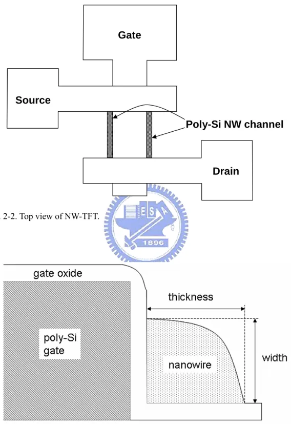
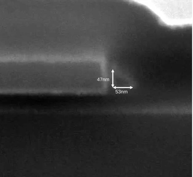
2-3 displays the definition of the nanowire thickness and width used in this study. An SEM picture of the device fabricated by SPC is shown in Fig. 2-4. The thickness and width of the device are 53nm and 47nm, respectively.
2.2 Electrical characterization and measurement
setup
Electrical characterizations were performed using an HP 4156 system. In all measurements, temperature-regulated hot chucks were used to control the temperatures.
In this study, threshold voltage (Vth) was calculated by the linear extrapolation
method [42]. Specifically, the threshold voltage was determined from the extrapolated
gate voltage VGi by
2
D T GiV
V
=
V
−
(2-1)where VGi was determined by the following steps: first, the point on the ID-VG curve
corresponding to the maximum in the transconductance (gm) was determined. Next, a
straight line across the point was used to extrapolate the ID-VG curve and locate the
intercept at the VG axis. In this work, VD was set at 0.5V.
The field-effect mobility in the test devices was determined from the
transconductance (gm) at VD = 0.5V by m FE ox D
Lg
WC V
µ
=
(2-2)increase in the weak inversion region by
(log
)
G DV
SS
I
∂
=
∂
(2-3)Chapter 3
Leakage current reduction in
NW-TFTs
3.1
Leakage mechanisms
According to the structure of the fabricated devices, there are two regions where leakage currents are likely to generate, i.e., the channel near the drain and the gate-to-drain overlap region. In this chapter we first briefly review possible mechanisms in these regions.
3.1.1 Leakage mechanisms in channel region
In poly-Si channels, the band diagram is modulated by the drain and gate biases. According to the strength of the electric field at the drain/channel junction, there are basically three conduction mechanisms illustrated in Figs. 3-1(a), (b), and (c).
(a) At a low drain field, the dominant leakage current mechanism is thermionic emission. This is due to thermal excitation of an electron from valence band into trap-state, and the trapped electron is emitted into conduction band by the same way.
(b) As the drain bias increases, the dominant leakage current mechanism is thermionic field emission. This case comprises two steps: the first step is the thermal activation of an electron from the valence band to a trap state, and the second step is electron
tunneling through the reduced barrier to the conduction band as shown in Fig. 3-1(b). (c) Under a strong electric field, the band gap is pulled more seriously. As a result
band-to-band tunneling becomes the dominant leakage current mechanism. It causes the electrons to tunnel from valence band to conductance band via the traps. .
According to Fig. 3-1 and the above discussions, these mechanisms all belong to trap-assisted leakage mechanisms. Hence the trap state density in the band gap plays an important role in the mechanism. The band-to-band current is strongly dependent on the applied bias. The pure thermal emission current is proportional to the intrinsic carrier
concentration of silicon (ni), and ni is proportional to exp [-Eg/2kT] (where Eg is the
energy band gap of silicon, k is the Boltzmann constant, and T is the temperature in Kelvin). For this reason, the activation energy of the pure thermal emission current
should be approximately equal to Eg/2. In addition, the pure thermal generation current is
nearly independent of gate voltage.
3.1.2 Leakage current mechanism in
gate-to-drain overlap region
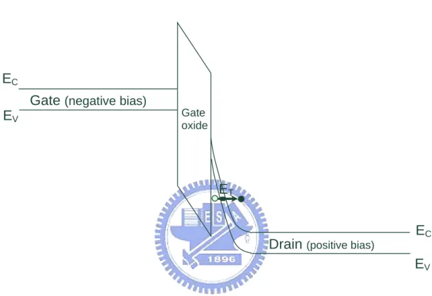
Another possible leakage current component occurring in the gate-to-drain overlap region is the gate induced drain leakage (GIDL). When the gate is negatively biased with respective to the drain and the voltage difference between the two is high, the n-type drain region overlapping the gate can be depleted and even inverted. As shown in Fig. 3-2,
when the potential difference between gate and drain (VGD) increases, the energy band is
avalanche multiplication, band-to-band tunneling and trap-assisted band-to-band tunneling. Hence a lot of extra minority carriers are generated and swept to the source to complete the path for GIDL.
There are many parameters that influence GIDL. VGD and the oxide thickness
between gate and drain are the two most important parameters in the GIDL mechanism because they directly govern the electric field in the depletion region. Another important parameter is the volume in which minority carriers are generated. In this regard, the gate-to-drain overlap area and the drain doping concentration are the two major factors. The drain doping concentration determines the depletion width in the gate-to-drain region. An increasing drain doping concentration leads to a decreasing depletion width, therefore the volume in which minority carriers are generated decreases. Besides, defects that cause necessary trap sites for assisting the leakage flow also play an important role in GIDL mechanism.
3.2
Effects of Si
3N
4hard mask layer
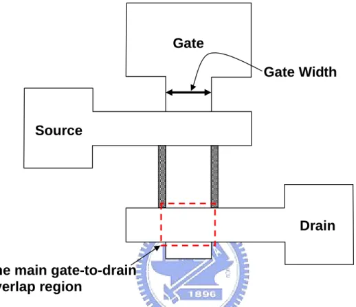
Figure 3-3 illustrates the gate-to-drain overlap region in the fabricated device. As has been identified in previous work [43], this unique feature in the proposed device structure actually contributes to the observed GIDL current. To reduce the GIDL, an extra
Si3N4 layer (HM) between gate and drain is added in this study to reduce the strength of
the electric field. Reduction of the electric field could help suppress the leakage, as mentioned in Section 3.1.2.
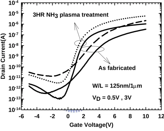
seen that with the 3hr NH3 plasma hydrogenation treatment, the electrical characteristics
of NW TFT with Si3N4 HM shows dramatic improvement as compared with the fresh
device. On-current, subthreshold swing and leakage current are all improved by the NH3
plasma hydrogenation. To clarify the exact region where the leakage current occurs, the
drain current (measured at maximum |VGD|) of the devices with various gate-to-drain
overlap areas are compared. Such analysis is helpful to understand the impact of the gate-to-drain overlap area, which is proportional to the width of the gate electrode as is evidenced by the top view of the device shown in Fig. 3-3, on the off-state leakage. The results are shown in Fig. 3-5. In this figure it is found that the off-state leakage currents for the devices with HM are nearly identical for devices with various gate-to-drain
overlap areas. Fig. 3-6(a) shows the drain current (measured at maximum |VGD|) as a
function of the gate width for NW TFTs with and without the Si3N4 HM, and the drain
current values normalized to that with minimum gate width (0.8 micron) are shown in Fig.
3-6(b). It can be seen that the drain current of NW TFTs with Si3N4 HM is almost
independent of the gate width. In contrast, the leakage current of NW TFTs without Si3N4
HM is strongly dependent on the gate-to-drain overlap area. From these results, we can
infer that the leakage current of NW TFTs without Si3N4 HM mainly occurs in the region
where the gate overlaps the drain, while the leakage current of NW TFTs with Si3N4 HM
mainly occurs in poly-Si nanowire channel.
We also extract the activation energy of devices to gain a deeper insight into the leakage mechanism. The activation energy is extracted using the following relation:
( ) 0 a E kT off
I
=
I e
− (3-1)energy.
The equation also can be expressed as
0
ln(
) ln( ) (
a)
offE
I
I
kT
−
=
+
(3-2)The drain current data measured at 25, 50, 75, 100, and 125 ℃ are exhibited in Fig. 3-7. Next, we use equation (3-2) to extract the activation energy. The extracted activation energies are summarized in Fig. 3-8. It can be seen that the activation energy of off-state
leakage for NW TFTs without Si3N4 HM shows a stronger dependence on the gate
voltage. The activation energy gradually decreases as the gate voltage becomes more
negative. In contrast, the activation energy of off-state leakage for NW TFTs with Si3N4
HM is nearly independent of the gate voltage, indicating that its dependence on the strength of electric field is also weak. In other words, GIDL is greatly suppressed in these
devices because Si3N4 HM can effectively shield the electrical field in the gate-to-drain
overlap region. Fig. 3-9 shows the band diagram in the gate-to-drain overlap region for
NW-TFTs with Si3N4 HM. Strength of electrical field at the Si/oxide interface in the
gate-to-drain overlap region is dramatically reduced due to the appearance of the Si3N4
HM.It is worth noting that even though the presence of Si3N4 HM effectively eliminates
the GIDL, the leakage current is still significant. A plausible reason is that the profile of
poly-Si nanowire channel may have been changed in devices with an extra Si3N4 HM
layer. Fig. 3-10 exhibits the cross-sectional picture of a device with HM. It is evidently seen that the poly-Si nanowire channel has a larger conduction width than the device without HM.
3.3
Effects of NH
3plasma hydrogenation
For operation of poly-Si TFTs, the conduction carriers in the channel have to overcome the barrier at the grain boundaries, the on-currents of the devices are dependent on the amount of defects contained [44]. In addition, the trap density is related to the leakage current as mentioned in Section 3.1. Therefore reducing trap density is a direct method to enhance the performance of TFTs. In this regard, hydrogenation is the most commonly used method to reduce the trap density in TFTs. It has been widely demonstrated that such approach could effectively passivate the dangling bonds at the grain boundaries as well as the intragrain strained bonds with hydrogen species.
Hydrogenation incorporation can be carried out by some different techniques, such
as hydrogen plasma [45], H+ implantation [46], hydrogen-rich Si3N4 capping layer [47]
and NH3 plasma [48]. In this work, we adopt the NH3 plasma treatment to achieve the
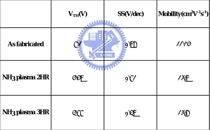
purpose. Fig. 3-11 presents the transfer characteristics of NW-TFTs with HM and
subjecting to various NH3 plasma times. Detailed data are summarized in Table 3-1. After
a 2hr NH3 plasma treatment, the device performance is apparently better than that of the
as-fabricated counterpart. Higher mobility, higher On/Off ratio and lower subthreshold
swing are observed after the plasma treatment, verifying the effectiveness of the NH3
plasma treatment.
3.4
Effects of RTA
was also explored to reduce the leakage current of NW TFTs. ID-VG characteristics of
devices with RTA are shown in Fig. 3-11. The NW-TFT with RTA obviously has better performance. This is believed to be due to the fact that the RTA process improves the
grain quality and thus reduces the defect density. Fig. 3-12 shows ID-VG characteristics of
devices with or without RTA treatment, all receiving an additional 2hr NH3 plasma
hydrogenation. NW-TFT with RTA still exhibits lower leakage current after plasma hydrogenation. Similarly, we have also measured the drain current of the control devices
(i.e., w/o Si3N4 hard mask) with various gate-to-drain overlap areas to analyze their
leakage mechanisms. These results are shown in Fig. 3-13 and Fig.3-14. As can be seen in these figures, although the off-state current of the NW TFTs with RTA is lower than that of their non-RTA counterparts, the dependence on the gate-to-drain overlap area is still evident. This phenomenon indicates that the gate-to-drain overlap zone is the region where the leakage current originates. The extracted activation energy is shown in Fig. 3-15 for NW-TFTs. The activation energy for NW-TFTs with RTA is significantly higher than the case without RTA treatment, albeit both are influenced by the gate voltage under off-state. It is suggested that although the leakage current is reduced, the GIDL remains the major mechanism in NW-TFT with RTA.
Chapter 4
NW-TFTs fabricated by MILC
4.1 Electrical characteristics of NW-TFTs
fabricated by MILC
The device structure is shown in Fig. 4.1. It was fabricated with similar process sequence as described in Chapter 2, except for the different treatments used for enhancing the film crystallization. The major steps are stated below: Briefly, after deposition of a 100nm-thick amorphous Si (a-Si) layer and subsequent S/D doping and patterning step, a 100nm-thick low-temperature oxide (LTO) was deposited by a plasma-enhanced (PE) CVD. For MILC purpose, the seeding windows were opened in the LTO layer. After opening the seeding windows, a 5nm-thick Ni layer was deposited to serve as the seeding
layer. The lateral crystallization was carried out at 550℃ for 16 hours in N2 ambient. The
arrows illustrated in Fig. 4-1 depict the crystallization paths. Fig. 4-2 exhibits the plane-view TEM of MILC NW-TFT. The NW channel is evidently laterally crystallized with large grain size, as shown in Fig. 4-2.
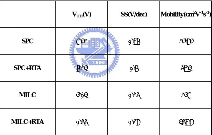
The transfer characteristics of n-type NW-TFTs fabricated by MILC are shown in Fig. 4-3. Detail electrical characteristics of devices are summarized in Table 4-1. The performance of the MILC device is obviously much better than that of the SPC device.
The extracted field-effect mobility is 247 cm2/V-sec for the MILC device, which is one
device is about 0.25 V/dec, much lower than that of the SPC counterpart (about 0.96 V/dec). The performance s is improved by the incorporation of an additional RTA process for both MILC and SPC devices. The MILC NW-TFTs still depict better electrical
characteristics including higher mobility, lower Vth, and lower SS as shown in Fig.4-4
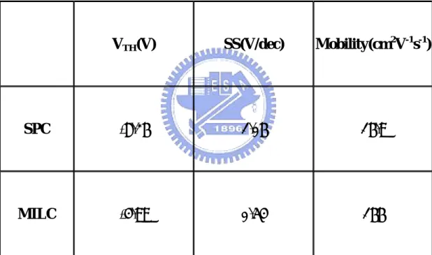
and Table 4-1. The poly-Si channels in MILC devices have larger grains and less grain boundaries that are transverse to the current flow than the SPC devices because of lateral crystallization. The number and height of barrier at grain boundaries which conduction carriers in channel must overcome are reduced so that the MILC NW-TFTs have better conduction behavior. Fig.4-5 and Table 4-1 compare the electrical characteristics between p-type NW-TFTs fabricated by either MILC or SPC scheme. Similar to n-type devices, the p-type MILC devices have much better performance than their SPC counterparts. Though the aforementioned enhancement in device performance is magnificent, the off-state leakage of the devices remains high despite the MILC treatment. This is likely to be due to potential Ni contamination. The formation of silicide at the grain boundaries during the MILC process has been reported previously [49], which would aggravate the leakage. This drawback could be alleviated by adopting the long Ni-offset structure [50] or by proper annealing condition [49].
4.2
Analysis for NW-TFTs with different MILC
seeding window arrangement
The location of MILC seeding window is very important because it can directly influence the electrical characteristics of devices. In this study, we exploit three splits of
samples as illustrated in Fig. 4-6 to address this issue. The splits are divided into two categories, namely, asymmetric and symmetric arrangements. In the symmetric case, two seeding windows are separately located at source and drain, while in the asymmetric case only one seeding window is situated at either source or drain.
Fig. 4-7 and Fig. 4-8 show the ID-VG characteristics of devices with asymmetric
seeding window at source and at drain, respectively. The data can be analyzed by dividing them into three regions. Since the poly-Si NW channels in all devices are the same, the properties are nearly identical in the on-region. In the off-region, the leakage current in the device with seeding window at drain is higher than that with seeding window at source. This is due to the fact that the MIC region is just situated at the gate-to-drain overlap region. The Ni concentration is higher in MIC region than MILC region, and there are many grain boundaries existing at the boundary between MIC region and MILC region. The Ni-related species that accumulate at the grain boundaries or inside the grains would cause a higher trap density in the gate-to-drain overlap region, and the leakage current of the device with seeding window at drain is therefore higher. In
the subthreshold region, the currents are nearly identical at VD=0.5V but the current in
NW-TFT with seeding window at drain is higher than the other at VD=3V. A plausible
reason is that the Ni concentration is higher near the seeding window. For the device with seeding window at drain, the Ni may produce more deep states near the drain edge. These
deep states may not be active at low field (i.e. VD=0.5V) but will serve as the trap sites
for trap-assisted tunneling current occurring at high field (i.e. VD=3V). As a result, the
subthreshold current becomes higher when the drain bias becomes larger.
symmetric seeding window is presented in Fig. 4-9. It is found that the device with asymmetric window at source has higher on-current and lower SS. The NW-TFTs with symmetric window have higher leakage current than NW-TFTs with asymmetric window at source. Note that in the MILC process, the crystallization proceeds radially from the seeding window. In the symmetric case, the fronts of crystallization from the opposite sides meet each other at the central region of the channel. Trace amount of metallic species may be left inside the channel, leading to the degraded on-state performance as compared with the asymmetric case.
Chapter 5
Conclusions
In this work, two methods were proposed to reduce the off-state leakage in the
newly-proposed NW-TFTs. The addition of an extra Si3N4 HM layer between the gate
and drain is found to effectively eliminate the GIDL occurring in the gate-to-drain overlap region, albeit the etched profile of poly-Si nanowire may need to be readjusted for optimization of the electrical characteristics. Finally, an additional RTA process is also found to effectively reduce the leakage current through the improvement of the thin-film quality, although GIDL still acts as the major leakage mechanism in the fabricated devices .
We have also employed the MILC method to improve the device characteristics. Film crystallinity of the NW fabricated by this method is shown to be dramatically improved. Needle-like larger grain structure with crystallization direction along the NW channel is demonstrated. This leads to a single-crystal-like structure and the device characteristics could be significantly improved in terms of extremely high carrier
mobility (>200 cm2/V-sec) and steeper subthreshold swing. Nevertheless, the Ni
contamination would cause leakage problem in our MILC devices. More efforts are needed to address this issue.
References:
[1] I. Yudasaka et al., “Polysilicon thin-film transistors,” Mat Res. Soc Symp. Proc., vol.182, pp.162, 1990.
[2] S. Wolf et al., “Silicon Processing for the VLSI Era,” Lattice Press, California, vol.1, chap.6, pp.161, 1986.
[3] S.D. Brotherton et al., “Polycrystalline silicon thin film transistors,” Semicond. Sci. Technol., pp.721-738, 1995
[4] C. H. Fa et al., “The polysilicon insulated-gate field-effect transistors,” IEEE Trans. Electron Devices, vol.13, pp.290, 1966.
[5] G.Baccarani et al., “Transport properties of polycrystalline silicon films,” J. Appl. Phys., vol.49, pp.5565-5570, 1978
[6] I.-W. Wu et al., “Mechanism and device-to-device variation of leakage current in polysilicon thin film transistors,” IEDM Tech. Dig., pp.867-870, 1990.
[7] J.R. Ayres et al., “Hot carrier effects in device and circuits formed from poly-Si,” IEE Proc. Circuit Device Syst., vol.141, pp.38-44, 1994.
[8] J. Ohwada et al., “Peripheral circuit integrated poly-Si TFT LCD with gray scale representation,” IEEE Trans. Electron Devices, vol.36, pp.1923-1928, 1989.
[9] A.G. Lewis et al., “Polysilicon TFT circuit design and performance,” IEEE J. Solid-State Circuit, vol.27, pp.1833-1842, 1992.
[10] S.D.S. Malhi et al., “Characteristics and three-dimensional integration of MOSFET's in small-grain LPCVD polycrystalline silicon,” IEEE Trans. Electron Devices, vol.32, pp.258-281, 1985.
[11] J. Levinson et al., “Concuctivity behavior in polycrystalline semiconductor thin film transistors,” J. Appl. Phys., vol.53, pp.1193-1202.
[12] J.G. Fossum et al., “Effects of grain boundaries on the channel conductance of SOI MOSFET’s,” IEEE Trans. Electron Devices, vol.30, pp.933-940, 1983.
[13] M.K. Hatalis et al., “Large grain polycrystalline silicon by low-temperature annealing of low-pressure chemical vapor deposited amorphous silicon films,” J. Appl. Phys., vol.63, pp.2260-2266, 1988.
[14] Y. Kawazu et al., “Low-temperature crystallization of hydrogenated amorphous silicon induced by nickel silicide formation,” Jpn. J. Appl. Phys., vol.29, pp.2698-2704, 1990.
[15] N. Kubo et al., “Characterization of polycrystalline-Si thin film transistors fabricated by excimer laser annealing method,” IEEE Trans. Electron Devices, vol.41, pp.1876-1879, 1994.
[16] I.-W. Wu et al., “Effects of trap-state density reduction by plasma hydrogenation in low-temperature polysilicon TFT,” IEEE Electron Devices Lett., vol.10, pp.123-125, 1989.
[17] I.-W. Wu et al., “Passivation kinetics of two types of defects in polysilicon TFT by plasma hydrogenation,” IEEE Electron Devices Lett., vol.12, pp.181-183, 1991. [18] G. Fortunato et al., “Field-effect analysis for the determination of gap-state density
and Fermi-level temperature dependence in polycrystalline silicon,” Phil. Mag. B., vol.57, pp.573, 1988.
[19] K. R. Olasupo et al., “Leakage current mechanism in sub-micron polysilicon thin-film transistors,” IEEE Trans. Electron Devices vol. 43, pp. 1218-1223, 1996.
[20] M. Yazaki et al., “Conduction mechanism of leakage current observed in metal-oxide-semiconductor transistors and poly-Si thin-film transistors,” Jpn. J. Appl. Phys. Vol. 31, pp. 206-209, 1992
[21] A. Bouhdada et al., “Modeling of gate induced drain leakage in relation to technological parameters and temperature,” 1997 Microelectron. Reliab. vol. 37, pp. 649-652, 1997.
[22] H.C. Lin et al., “Nanoelectronic technology: in search of the ultimate device structure,” in Future Trends in Microelectronics: the Nano Millennium, S.Luryi, J.M. Xu, and A. Zaslavsky, eds., pp.4-14 (New York: Wiley 2004).
[23] X. Duan et al., “Nonvolatile memory and programmable logic from molecule-gated nanowires,” Nano Letters, vol.2, pp.487-490, 2002.
[24] X. Duan et al., “High-performance thin-film transistors using semiconductor nanowires and nanoribbons,” Nature, vol.425, pp.274-278, 2003.
[25] Y. Cui et al., “Nanowire nanosensors for highly sensitive and selective detection of biological and chemical species,” Science, vol.293, pp.1289-1292, 2001.
[26] X. Duan et al., “Indium phosphide nanowires as building blocks for nanoscale electronic and optoelectronic devices,” Nature, vol.409, pp.66-69, 2001.
[27] Y. Huang et al., “Directed assembly of one-dimensional nanostructures into functional networks,” Science, vol.291, pp.630-633, 2001.
[28] A. Tao et al., “Langmuir-Blodgett silver nanowire monolayers for molecule sensing using surface-enhanced Raman spectroscopy,” Nano Lett., vol. 3, pp. 1229-1233, 2003.
pp.6394-6399, 1991
[30] B. Mohadjeri et al., “Nickel-enhanced solid-phase epitaxial regrowth of amorphous silicon,” Phys. Rev. Lett., vol.68, pp.1872-1875, 1992.
[31] Z. Jin et al., “Solid-phase reaction of Ni with amorphous SiGe thin film on SiO2,”
Jpn. J. Appl. Phys., vol.36, pp.L1637-L1640, 1997.
[32] C. Hayzelden et al., “In-situ transmission electron microscopy studies of silicide-mediated crystallization of amorphous silicon,” Appl. Phys. Lett., vol.60, pp.225-227, 1992.
[33] Z. Tan et al., “Gold induced gemanium crystallization,” Phys. Rev. B, vol.46, pp.9505-9510, 1992.
[34] S.-W. Lee et al., “Low temperature poly-Si thin-film transistor fabrication by metal-induced lateral crystallization,” IEEE Electron Device Lett., vol.17, pp.160-162, 1996.
[35] S.-W. Lee et al., “Fabrication of high-mobility p-channel poly-Si thin film transistors by self-aligned metal-induced lateral crystallization,” IEEE Electron Device Lett., vol.17, pp.407-409, 1996.
[36] T. Ma et al., “Dopant and thickness dependence of metal-induced lateral crystallization of amorphous silicon films,” J. Appl. Phys., vol.91, pp.1236-1241, 2002.
[37] G. Bhat et al., “Effect of MIC/MILC interface on the performance of MILC-TFT’s,” in Dig. 56th Annu. Device Research Conf., pp.110-111, 1998.
[38] Z. Jin et al., “Nickel induced crystallization of amorphous silicon thin films,” J. Appl. Phys., vol.84, pp.194-100, 1998.
[39] G. Bhat et al., “Analysis and reduction of kink effect in MILC-TFT’s,” in Proc.18th Int. Display Research Conf., pp.433-436, 1998
[40] Z. Meng et al., “High performance low temperature metal-induced unilaterally crystallized polycrystalline silicon thin film transistors for system-on-panel applications,” IEEE Trans. Electron Devices vol. 47, pp. 404-409, 2000.
[41] H. C. Lin et al., “A simple and low-cost method to fabricate TFTs with poly-Si nanowire channel,” IEEE Electron Device Lett., vol. 26, pp.643-645, 2005.
[42] ASTM Standard F617M-95, “Standard method for measuring MOSFET linear threshold voltage,” 1996 Annual Book of ASTM Standards, Am. Soc. Test. Mat., Conshohocken, PA, 1996.
[43] H. T. Lin, “Fabrication and Characterization of a Novel Polycrystalline Silicon Thin Film Transistor with Nanowire Channels,” MS, thesis, Dept. Electronics, Eng, Chiao-Tung University, Hsinchu, Taiwan, 2003
[44] John Y. W. Seto, “The electrical properties of polycrystalline silicon films,” J. Appl. Phys., vol. 46, pp. 5247-5254, 1975.
[45] T. I. Kamins et al., “Hydrogenation of transistors fabricated in polycrystalline-silicon films,” IEEE Electron Device Lett., vol.1, pp.159-161, 1980.
[46] M. Rodder et al., “Effects of H+ implant dose and film deposition conditions on
polycrystalline-Si MOSFET characteristics,” IEEE Electron Device Lett., vol.8, pp.27-29, 1987.
[47] G. P. Pollack et al. “Hydrogen passivation of PolySilicon MOSFET's from a plasma Nitride source,” IEEE Electron Device Lett., vol.5, pp.468-470, 1984.
silicon thin-film transistors,” IEEE Trans. Electron Devices vol. 44, pp. 64-68, 1997. [49] C. K. Chan et al., “Effects of dopants on the electrical behavior of grain boundary in metal-induced crystallized polysilicon film,” IEEE Trans. Electron Devices, vol. 52, pp. 1917-1919, 2005.
[50] Gi. B. Kim et al., “Electrical characteristics of MILC poly-Si TFTs with long Ni-offset structure,” IEEE Trans. Electron Devices, vol. 50, pp. 2344-2347, 2003.
Table 3-1. Electrical characteristics of as-fabricated device and devices which received
2-hr and 3-hr NH3 plasma treatment.
V
TH(V)
SS(V/dec)
Mobility(cm
2V
-1s
-1)
As fabricated
7.1
0.98
11.24
NH3 plasma 2HR
4.49
0.71
15.9
Table 4-1. Comparisons of device parameters between n-type SPC and MILC NW-TFTs.
V
TH(V)
SS(V/dec)
Mobility(cm
2V
-1s
-1)
SPC
7.42
0.96
24.84
SPC+RTA
6.23
0.6
59.3
MILC
4.03
0.25
247
MILC+RTA
0.55
0.18
359.8
Table 4-2. Comparisons of device parameters between p-type SPC and MILC NW-TFTs.
V
TH(V)
SS(V/dec)
Mobility(cm
2V
-1s
-1)
SPC
-8.26
1.06
16.9
Fig. 2-2. Top view of NW-TFT.
Fig. 2-3. The definition of the poly-Si nanowire channel.
Source
Drain
Gate
Fig. 2-4. SEM picture of a device fabricated by SPC.
47nm
Fig. 3-1. Leakage mechanisms in channel. (a) Thermionic emission. (b) Thermioic field emission. (c) Band-to-band tunneling.
EC EV Drain Channel E T EC EV Drain Channel ET EC EV Drain Channel ET (a) (b) (c)
Fig. 3-2. Band diagram illustrating GIDL occurrence.
E
VGate
(negative bias)E
CDrain
(positive bias)E
TE
CE
V GateFig. 3-3. Schematic layout illustrating the gate-to-drain overlap region.
Source
Drain
Gate
Gate Width
The main gate-to-drain
overlap region
Fig. 3-4. Transfer characteristics of NW-TFTs with HM, both with and without plasma treatment.
Gate Voltage(V)
-6
-4
-2
0
2
4
6
8
10
12
Drain Cur
rent(A)
10
-1410
-1310
-1210
-1110
-1010
-910
-810
-710
-610
-510
-43HR NH3 plasma treatment
As fabricated
W/L = 125nm/1
µm
VD = 0.5V , 3V
Fig. 3-5. Leakage currents of NW TFTs with HM having various gate widths.
VG (V)
-6
-4
-2
0
2
I D
(A)
10
-1110
-1010
-910
-8 GW = 0.8µm GW = 1µm GW = 2µm GW = 5µm VD = 5VFig. 3-6. (a) comparison of leakage currents of NW TFTs with and w/o HM having various gate widths, (b) comparison of the normalized off-state current for
devices with and w/o HM as a function of gate width. |VGD| = 10 V.
Gate Width(µm) 0 1 2 3 4 5 6 Dra in c u rre n t( A ) 0.0 5.0e-11 1.0e-10 1.5e-10 2.0e-10 2.5e-10 3.0e-10 NW-TFT with HM NW-TFT w/o HM VD = 5V VG = -5V Gate Width(µm) 0 1 2 3 4 5 6 I D / ID (gat e w idt h =0 .8 µm) 0 2 4 6 8 NW-TFT with HM NW-TFT w/o HM VD = 5V VG = -5V (a) (b)
Fig. 3-7. Transfer characteristicsof NW-TFT with HM at various temperatures.
Gate Voltage(V)
-6
-4
-2
0
2
4
6
Drain Current(A)
10
-1210
-1110
-1010
-910
-810
-710
-610
-5 25 oC 50 oC 75 oC 100 oC 125 oC VD = 3VFig. 3-8. Off-state activation energies of NW-TFTs with and without HM.
Gate Voltage(V)
-6
-5
-4
-3
-2
-1
0
A
c
ti
vati
on E
nergy
(eV
)
0.0
0.1
0.2
0.3
0.4
0.5
0.6
NW-TFT with HM
NW-TFT w/o HM
VD = 3VFig. 3-9. Energy band diagram in gate-to-drain overlap region for NW-TFTs with HM.
Gate
(negative bias)E
CE
VDrain (positive bias)
E
CE
VLower electrical field
Gateoxide
Si3N4
Fig. 3-10. TEM of NW-TFT with HM.
125nm
Fig. 3-11. Transfer characteristics of as-fabricated device and devices which received 2-hr
and 3-hr NH3 plasma treatment at (a) VD=0.5V, (b) VD=3V
Gate Voltage(V) -6 -4 -2 0 2 4 6 8 10 12 Drain Curr ent(A) 10-14 10-13 10-12 10-11 10-10 10-9 10-8 10-7 10-6 10-5 As fabricated NH3 plasma 2HR NH3 plasma 3HR Gate Voltage(V) -6 -4 -2 0 2 4 6 8 10 12 Dra in C u rr en t( A) 10-12 10-11 10-10 10-9 10-8 10-7 10-6 10-5 10-4 As fabricated NH3 plasma 2HR NH3 plasma 3HR (a) (b)
Fig. 3-12. Transfer characteristics of control NW-TFTs.
Gate Voltage(V)
-6
-4
-2
0
2
4
6
8
10
12
Dr
ain Curr
ent(A)
10
-1510
-1410
-1310
-1210
-1110
-1010
-910
-810
-710
-610
-5with RTA
w/o RTA
W/L = 45nm/1
µm
VD = 0.5V , 3V
Fig. 3-13. Off-state ID-VG characteristics of NW-TFTs after 2hr-NH3 plama treatment.
Gate Voltage(V)
-6
-4
-2
0
2
Drain
cu
rren
t(A)
10
-1410
-1310
-1210
-1110
-1010
-910
-8w/o RTA
with RTA
VD = 0.5V , 3V
Fig. 3-14. Off-state currents of control NW-TFTs (w/o Si3N4 mark mask) having various gate widths.
Gate Voltage(V)
-6
-4
-2
0
2
4
Drai
n Cu
rrent
(A)
10
-1210
-1110
-1010
-910
-8GW=0.8
µm
GW=1
µm
GW=2
µm
GW=5
µm
W/L = 45nm/1
µm
VD = 5V
Fig. 3-15. (a) comparison of leakage currents of NW TFTs with and w/o RTA having various gate widths, (b) comparison of the normalized off-state current for
devices with and w/o RTA as a function of gate width. |VGD| = 10 V.
Gate Width(µm)
0
1
2
3
4
5
6
Dr ain Cur rent(A)0.0
5.0e-11
1.0e-10
1.5e-10
2.0e-10
2.5e-10
3.0e-10
NW-TFT with RTA NW-TFT w/o RTA VD = 5V VG = -5V Gate Width(µm) 0 1 2 3 4 5 6 I D /ID (gate w idth = 0 .8 µm) 0 1 2 3 4 5 6 7 8 NW-TFT with RTA NW-TFT w/o RTA VD = 5V VG = -5VFig. 3-16. Off-state activation energies of NW-TFTs with and without RTA.
Gate Voltage(V)
-6
-5
-4
-3
-2
-1
0
Activa
tion E
n
er
gy
(e
V)
0.0
0.1
0.2
0.3
0.4
0.5
0.6
0.7
NW-TFT with RTA
NW-TFT w/o RTA
VD = 3VFig. 4-1. Crystallization mechanism of MILC. The arrows represent the crystallization direction.
Fig. 4-2. The plane-view TEM of MILC NW-TFT.
Poly-Si NW
Gate
Fig. 4-3. Comparison of transfer characteristics between n-type MILC and SPC NW-TFTs.
Gate Voltage(V)
-6
-4
-2
0
2
4
6
8
10
12
Drain Current(A)
10
-1510
-1410
-1310
-1210
-1110
-1010
-910
-810
-710
-610
-510
-4 NW-TFT fabricated by MILC NW-TFT fabricated by SPC VD = 0.5V,3VFig. 4-4. Comparison of transfer characteristics between n-type MILC and SPC NW-TFTs with RTA.
Gate Voltage(V)
-6
-4
-2
0
2
4
6
8
10
12
Drain Current(A)
10
-1610
-1510
-1410
-1310
-1210
-1110
-1010
-910
-810
-710
-610
-510
-410
-3 NW-TFT fabricated by MILC NW-TFT fabricate by SPC VD = 0.5V,3VFig. 4-5. Comparison of transfer characteristics between p-type MILC and SPC NW-TFTs
Gate Voltage(V)
-12
-10
-8
-6
-4
-2
0
2
4
6
Drain Current(A)
10
-1510
-1410
-1310
-1210
-1110
-1010
-910
-810
-710
-610
-510
-4 NW-TFT fabricated by MILC NW-TFT fabricated by SPC VD = 0.5V,3VFig. 4-6. Configurations of MILC seeding window. (a) Asymmetric seeding window (at source). (b) Asymmetric seeding window (at drain). (c) symmetric seeding window. Source Drai Gate seeding window Source Drain Gate seeding window Source Drain Gate seeding window (a) (b) (c)
Fig. 4-7. ID-VG characteristics of devices fabricated by asymmetric MILC seeding window.
Gate Voltage(V)
-6
-4
-2
0
2
4
6
8
10
12
Drain Current(A)
10
-1510
-1410
-1310
-1210
-1110
-1010
-910
-810
-710
-610
-510
-410
-3 seeding window at S seeding window at D VD = 0.5V,3VFig. 4-8. ID-VG characteristics of RTA devices fabricated by asymmetric MILC seeding window.
Gate Voltage(V)
-6
-4
-2
0
2
4
6
8
10
12
Drain Current(A)
10
-1610
-1510
-1410
-1310
-1210
-1110
-1010
-910
-810
-710
-610
-510
-410
-3 seeding window at S seeding window at D VD = 0.5V,3VFig. 4-9. Comparison of ID-VG characteristics between devices fabricated by asymmetric
and symmetric seeding window configuration.
Gate Voltage(V)
-6
-4
-2
0
2
4
6
8
10
12
Drain Current(A)
10
-1510
-1410
-1310
-1210
-1110
-1010
-910
-810
-710
-610
-510
-410
-3Asymmetric seeding window at S Symmetric seeding window