行政院國家科學委員會專題研究計畫期中報告
具有低介電常數阻障介電薄膜製程整合之研究 (1/2)
Study on the integration of barrier dielectric with low dielectric
constant (1/2)
計畫編號:NSC 91-2215-E-009-041
執行期間:91 年 8 月 1 日至 92 年 7 月 31 日
計畫主持人:施 敏
共同主持人:張鼎張
計畫參與人員:莫亦先 國立交通大學電子研究所
蔡宗鳴 國立交通大學電子研究所
林宗衛 國立交通大學電子研究所
一、 中文摘要 當元件結構隨之縮小時,內層導線間的 距離愈來愈接近,由導線電阻與導線結構間 之 電 容 所 形 成 之 訊 號 傳 輸 延 遲 (RC delay) ,已大大降低其元件的切換性能。為 了增加積體電路的速度,降低導線阻值與導 線間的電容值,皆是不錯的方法。而研究發 現,當低介電常數材料與銅整合時,銅會擴 散至介電層中降低其品質。為了克服此一問 題,具有低介電常數值的阻障介電層(barrier dielectric)的研究於是因應而生。其中以碳化 矽(SiC) 阻障介電層具有較氮化矽(k~7)低 的介電常數(k~5)最受矚目。在本年度計畫 中,主要探討不同氮掺雜含量的SiC 的介電 特性及材料特性,我們發現擁有較高氮含量 的SiC 呈現較好的阻障介電特性。此外,根 據SIMS 的材料分析,發現經由 BTS 的可靠 度測試後的 SiC 其介電崩潰主要是由於 Cu 金屬穿透整個SiC 阻障介電層的原故。 AbstractTo reduce the RC delay of interconnects, the low-k dielectrics and Cu interconnects must be adopted. SiC is a candidate for barrier dielectric and owns lower dielectric constant (k~5) related to SiN (k~7).
In this study, we investigate the leaky behavior and barrier characteristics of SiC (k:4~5) doped with different nitrogen concentrations. We find that SiC films contained higher nitrogen concentration exhibit better barrier property. According to the SIMS analysis, the copper penetrates through the SiC film as the SiC is breakdown during BTS test.
二、前言與目的
A continue reduction in chip size and increase in chip complexity is shifting the interconnection technology towards multilevel metallization. As the dimension of device scales down, the spaces between interconnect lines become closer. Therefore, the RC delay caused by the resistance of Al conductors and the capacitance of the structures with
SiO2-based dielectrics is no longer neglected.
In deep submicron region, it is necessary to reduce the resistivity of interconnection by implementation of new materials. Copper is
attracting interest as an interconnection material for future high speed ULSIs because of its low electrical resistivity and high resistance to electron and stress migration [1]. In addition, a lower dielectric constant insulator is needed to counter the problems of parasitic capacitance delays and cross talk across layers. However, copper diffusion into dielectric film is an important issue when copper is integrated in the interconnect structure [2]. Therefore, Barrier dielectric film is developed in order to block copper diffusion in dielectric film [3-4]. The conventional barrier dielectric is SiN which could efficiently prevent the Cu drift [5]. However, the dielectric constant of SiN is lager than oxide. To reduce the effective dielectric constant of IMD and ILD, SiN must be substituted [6]. Studying on barrier dielectrics which own lower dielectric constant related to SiN is attractive. SiC-related dielectrics are the most candidates of the barrier dielectrics. In this study, we investigated the SiCN which owns lower dielectric constant than SiN. The films with various nitrogen-containing have different barrier ability. We use the planar metal-insulator-semiconductor (MIS) capacitors to realize the reliabilities of SiCN
with Cu by electrical and material analysis. 三、研究方法
The silicon carbide films with various
nitrogen additives were deposited with tri-methyl-silane source. The deposition
temperature is about 350oC. Various
concentrations of nitrogen were controlled by
NH3 gas flow rate during deposit process. The
silicon carbide film was deposited on p-type silicon wafer with a resistivity of 15-25 Ω-cm.
The code name of the pure silicon carbide film in this study is “SiC”. In addition, the code names of silicon carbide films with various
flow rate of NH3 gas are “SiC-N1”, “SiC-N2”,
“SiC-N3” and “SiC-N4”. The flow rate of
NH3 gas for SiC-N1, SiC-N2. SiC-N3 and
SiC-N4 were increasing from 250 to 500 sccm. The XPS (X-ray photoelectron spectra) was recorded by a VG Escalab MKII spectrometer using Mg Kα (1253.6eV) radiation, and it was employed to observe the composition of silicon carbide films. The infrared spectrometry was performed from 4000 to 400
cm-1 using a Fourier transform infrared (FTIR)
spectrometer calibrated to an unprocessed bare wafer, for determining the chemical structure of the silicon carbide film. The refractive index and thickness of the silicon carbide with or without nitride additive were measured with an n&k analyzer and SORRA ellipsometer. MIS structures of Cu/silicon carbide/silicon as well as Al/silicon carbide/silicon were used to investigate the behavior of basic electrical characteristic.
The dielectric constants and leakage current of the SiC films were investigated according to the measurement of capacitance-voltage (C-V) and current-voltage (I-V) characteristics by using a metal-insulator-semiconductor (MIS) capacitor structure. A Keithley Model 82 CV
meter was used to measure the dielectric constant of the film with a gate electrode area
of 0.0053 cm2, which was measured at 1 MHz.
The leakage current-voltage (I-V) characteristics of SiC films were also measured by HP4156. The gate-electrode area
of the MIS structure was 0.00133 cm2 for I-V
measurement.
The completed Al and Cu gated MIS capacitors were then bias-temperature-stressed
(BTS) at 150oC with gate electrode biases
(Vgate). The stress time was 1000 sec, which is
long enough for the mobile charges to drift across the stacked insulator layer. The bias was provided by an HP4156B semiconductor parameter analyzer.
四、結果與討論
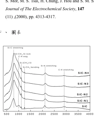
Figure 1 shows FTIR spectra of silicon carbide films without and with the various
flow rate of NH3 gas during deposit process,
and the important regions of silicon carbide film were labeled in the figure and indicated
as followed. The peak at 780 cm-1 is identified
as Si-C stretching bond. In addition,
Si-CH2-Si rock and C-H wag peak are near
990 cm-1, C-F bending peak is at 1100 cm-1,
Si-CH3 bending peak is at 1245 cm-1, Si-H
stretching peak is near 2100 cm-1, and C-H
stretching peak is near 2960 cm-1. All of these
bonds make the surface of the silicon carbide film hydrophobic. From the figure, there was not any nitride derivatives or nitride in all samples, and it was obvious that SiC-N1~SiC-N4 have the stronger Si-C stretching bonds than the pure silicon carbide, SiC.
XPS spectra for all of the specimens are
showed in Fig. 2, and the major peak for Si2p
(~115eV), Si2s (~145eV) and C1s (~285eV) of
every specimens are clearly evident in it. The
peak of N1s (~398eV) appears in
SiC-N1~SiC-N4, but was absent in pure
silicon carbide, SiC. The enlargement of N1s
for all the specimens are showed in Fig. 3. It certificates the existence of SiN bonding in SiCN samples. The peak heights of SiC-N1~ SiC-N4 raise greatly than that of SiC. On the contrary, the carbon contents of the sample SiC-N1~SiC-N4 are smaller than that of the
sample SiC. Moreover, the content of silicon remains constant for all the specimens.
The refractive index (n) and dielectric constant (k) values for all of the specimens were demonstrated in Fig. 4. The pure silicon carbide (SiC) film had a refractive index of
1.88, and the silicon carbide films with NH3
gas flow during depositing process have a larger refractive index from 1.89 to 1.95. The pure silicon carbide film had a dielectric constant about 3.8, and the dielectric constants of nitrogen-containing films, SiCN, were from 4.3 to 4.9. Anyhow, we found that the dielectric constant and the refractive index of
silicon carbide with NH3 gas flow during
PECVD process (SiC-N1 ~ SiC-N4) are larger than the pure one, SiC.
The leakage current densities for all of the films are sketched in Fig.5. It was showed clearly that the leakage current of pure silicon carbide (SiC) is much lager than other SiCN films. The curves of SiC-N1~SiCN4 are almost similar so that we can put them on a par. Increasing the temperature increase the leakage current density. Furthermore, the J-E curves are symmetric both in positive and negatives bias, and the mechanism of leakage current is Poole-Frenkel (P-F) emission as the electrical filed is above 2.5MV/cm. Poole-Frenkel (P-F) [7] emission is due to field-enhanced thermal excitation of trapped electrons in the insulator into the conduction band. The current density is given by:
− = T k E J J B PF PF φ β 1/2 0exp
The theoretical value of β consists with the experimental one in our study.
We investigate the impacts of thermal annealing on the silicon carbide films, so the silicon carbide film, SiC-N4, was transferred into furnace at the temperature from 400 to
550oC for more than 1 hour in N2 ambient. Figure 6 shows the J-E curves of SiC-N4 with Cu gate before and after thermal annealing treatment at the temperature from 400 to
550oC for more than 1 hour. There is almost
no division between the leakage current after thermal annealing and the standard data. In the other hand, the FTIR spectrum doesn’t vary after thermal treatment. Then, thermal
treatment at the temperature till 550oC doesn’t
have obvious effect on the silicon carbide film. The other nitrogen-containing films also have the same manner. Consequently, the thermal stability of silicon carbide film is good enough to meet the prescription in BEOL fabrication process.
SiCN film exhibit an excellent electrical property, such as the leakage current doesn’t show distinct variations after BTS (3MV/cm,
150oC, 1000sec). Figure 7 and 8 exhibit the
Igate-tstress curves of SiC-N1 and SiC-N4 with
either Al or Cu gate during BTS measurement. Compared Fig. 7 to 8, it’s evident that the leakage current of SiC-N1 was almost one magnitude more than that of SiC-N4. The leakage current becomes lowering and saturation in the electric field below 3.50 MV/cm when stress time goes through, but goes up in the electric field greater than 3.75 MV/cm. The leakage currents even increase abruptly that we can gauge it as breakdown respectively, when the electric fields are greater than 4.5 MV/cm for SiC-N1 and 5.0 MV/cm for SiC-N4.
In the cause of finding out the factors making the difference between the increasing and saturation behaviors of leakage currents, certain kind of material analysis were excused. Figure 9 and 10 illustrated the SIMS spectrum of SiC-N4 with either Cu or Al electrode after BTS measurement in the condition of 3.5 and
5.0 MV/cm for 1000sec at 150oC. It’s clear
that the copper counts in the SiCN layer of the MIS structure after 5.0 MV/cm BTS is much larger than that after 3.5 MV/cm BTS, which almost remains zero. Furthermore, the Al counts remained deficient in the silicon carbide layer of the MIS structure not only in the specimen after 3.5 MV/cm BTS but also 5.0 MV/cm BTS, simultaneously.
五、計畫成果自評
In this project, we have investigated the dielectric intrinsic behavior and barrier characteristics of SiC (k:4~5) doped with different nitrogen concentrations. The leakage behavior of SiC is Poole-Frenkel in high field. This is similar to SiN. We perform the bias-temperature stress (BTS) on SiC to test the barrier ability against copper penetration. We find that the SiC doped with nitrogen could sustain the stress of electrical field up to
4MV/cm at 150oC. This experimental results
show that SiC films contained higher nitrogen concentration exhibit better barrier property against copper penetration.
六、參考文獻
[1] T. Sakurai, “Closed-form expressions for interconnection delay, coupling and crosstalk in VLSI’s”, IEEE trans. Elec. Devices, 40, (1993), pp.118
[2] A. Mallikarjunan, S. P. Murarka, and T.-M. Lu,” Metal drift behavior in low dielectric constant organosiloxane polymer”, Appl. Phys. Lett.,79, (2001),1855
[3] M. Vogt, M. Kachel, K. Drescher, “Dielectric Barrier for Cu Metallization System”, Materials for
Avanced Metallization, (1997), pp.51
[4] Soo Geun Lee, Yun Jun Kim, Seung Pae Lee, Hyeok-Sang Oh, Seung Jae Lee, Min Kim, Il-Goo
w a v e n u m b e r ( c m- 1 ) 5 0 0 1 0 0 0 1 5 0 0 2 0 0 0 2 5 0 0 3 0 0 0 3 5 0 0 4 0 0 0 S i C S i C - N 1 S i C - N 2 S i C - N 3 S i C - N 4 S i- C s tr e tc h in g S i- C H3 b e n d in g S i- C H3- S i r o c k C - H w a g S i- ( C H2) - S i S i- H s tr e tc h in g C - H s tr e tc h in g
Binding energy (eV)
0 200 400 600 800 1000 1200 1400 a. u . Si2pSi 2SC 1S N 1S O 1S O KL1O KL2N KL1 C KL2
Kim, JaeHak Kim, Hong-Jae Shin, Jin-Gi Hong, Hyeon-Deok Lee and Ho-Kyu Kang .“Low dielectric constant 3MS α-SiC:H as Cu diffusion barrier layer in Cu dual damascene process”, Jpn. J.
Appl. Phys. ,(2001),Vol.40 Part.1, No.4B,
pp.2663-2668,
[5] Masayuki Tanaka, Shigehiku Saida, Tadashi Lijima and Yoshitaka Tsunashima, “Low-k SiN films for Cu interconnects integration fabricated by ultra low temperature thermal CVD”, Symposium on VLSI
Technology Digest of Technical Papers, (1999),
pp.47-48
[6] M. Tada, Y. Harada, K. Hijioka, H. Ohtake, T.Takeuchi, S. Saito, T. Onodera, M. Hiroi, N. Furutake and Y. Hayashi, Cu Dual Damascene Interconnects in Porous Organosilica film with organic Hand-mask and Etch-stop layers For 70nm-node ULSIs”, proc.
IITC2002,(2002),pp12-14
[7] S. M. Sze, Physics of Semiconductor Devices, Ch. 7, pp. 402, Wiley, New York (1981).
[8] P. T. Liu, T. C. Chang, M. C. Huang, Y. L. Yang, Y. S. Mor, M. S. Tsai, H. Chung, J. Hou and S. M. Sze,
Journal of The Electrochemical Society, 147
(11) ,(2000), pp. 4313-4317.
七、 圖表
Figure 1 FTIR spectra of silicon carbide with or without NH3 gas flow during deposit process.
Figure 2 XPS (X-ray photoelectron spectra) spectra for all of the specimens.
Figure 3 Enlargement of XPS spectra ranging of N1S of
all specimens.
Figure 4 Refractive indexes (n) and dielectric constants (k) for all of the specimens
Binding energy (eV)
390 395 400 405 a. u. SiC SiC-N1 SiC-N2 SiC-N3 SiC-N4 N
D ep th profile (nm ) 0 25 50 75 100 125 150 S e c ondar y I on C ount s 100 101 102 103 104 105 C u 5M V /cm C u 3.5M v/cm S iC N S i E ( M V /c m ) - 5 - 4 - 3 - 2 - 1 0 1 2 3 4 5 J ( A /c m 2) 1 0- 9 1 0- 8 1 0- 7 1 0- 6 1 0- 5 1 0- 4 1 0- 3 1 0- 2 S iC S iC - N 1 S iC - N 2 S iC - N 3 S iC - N 4 Depth profile (nm) 0 25 50 75 100 125 150 S e co nd ar y I o n C o un ts 100 101 102 103 104 105 Al 5MV/cm Al 3.5MV/cm SiCN Si
Figure 5 J-E curves for all of the samples.
Figure 6 J-E curves for all of the samples after thermal annealing
Figure 7 Leakage current-stress time curves of SiC-N1 with Cu/Al gates during BTS
Figure 8 Leakage current-stress time curves of SiC-N4 with Cu/Al gates during BTS.
Figure 9 SIMS depth profile of SiCN4 with Al gate after BTS measurement (3.5/5MV/cm, 150oC, 1000sec)
Figure 10 SIMS depth profile of SiCN4 with Cu gate after BTS measurement (3.5/5MV/cm, 150oC, 1000sec)
E (MV/cm) 0 1 2 3 4 5 J ( A /c m 2) 10-10 10-9 10-8 10-7 10-6 10-5 10-4 10-3 10-2 STD 400o C 450o C 500o C 550oC A l 4.5M V/cm
Stress Tim e (sec)
0 200 400 600 800 1000 Le ak age C u rr e n t ( A ) 0 10-4 2x10⁻⁴ 3x10⁻⁴ 4x10⁻⁴ 5x10⁻⁴ A l 5M V/cm A l 5.5M V/cm C u 4.5M V/cm Cu 5.5M V/cm Cu 5M V/cm S tre s s T im e (s e c ) 0 2 0 0 4 0 0 6 0 0 8 0 0 1 0 0 0 Le ak ag e C u rr e n t ( A ) 0 1 0-4 2 x 1 0-4 3 x 1 0-4 4 x 1 0-4 5 x 1 0-4 C u 4 .5 M V /c m C u 5 .5 M V /c m C u 5 M V /c m A l 4 .5 M V /c m A l 5 M V /c m A l 5 .5 M V /c m