國立交通大學
材料科學與工程學系
博士論文
分子束磊晶低溫成長 III-V 族稀磁半導體之結構與性質
Structures and properties of III-V diluted magnetic semiconductors
grown by low temperature molecular beam epitaxy
研究生:李薇妮
分子束磊晶低溫成長 III-V 族稀磁半導體之結構與性質
Structures and properties of III-V diluted magnetic semiconductors
grown by low temperature molecular beam epitaxy
研究生:李薇妮 Student : Wei-Ni Lee
指導教授:郭正次博士 Advisor: Dr. Cheng-Tzu Kuo
國立交通大學
材料科學與工程學系
博士論文
A Dissertation
Submitted to Department of Materials Science and Engineering, College of Engineering
National Chiao Tung University In Partial Fulfillment of the Requirements
For the Degree of Doctor of Philosophy
in
Materials Science and Engineering January 2006
分子束磊晶低溫成長 III-V 族稀磁半導體之結構與性質
研究生:李薇妮 指導教授:郭正次博士
國立交通大學材料科學與工程學系
摘 要
III-V 族半導體廣為應用在光電及快速元件。然而,同時具有半導體傳導特性與磁 性之奈米薄膜,因具有降低元件膜層間自旋電子散射之特性,而成為可應用在自旋電子 元件的重要關鍵技術之一。在傳統的半導體材料中加入少量磁性元素,形成所謂稀磁半 導體(DMS),例如將 Mn 原子加入傳統的 III-V 族半導體,即屬於此類應用而新發展的 材料。本實驗成功的在GaAs 與 InP 基材上,生長系列稀磁半導體多層膜,並研究其結 構與性質。不同於傳統磊晶的生長方法,利用分子束磊晶低溫(<300℃)成長,降低沉 積時原子間互相擴散而形成介穩態,較傳統方法可加入較高含量的磁性原子以增加其磁 性。利用TEM、DXRD、EPMA 與 SQUID 研究其結構與性質,實驗結果略分為三類: 1、LT-GaAs磊晶層中過量砷析出行為的研究,發現不同方向的GaAs基板之磊晶層中過 量砷濃度在GaAs(311)B> (311)A> (001)。可能因晶面配位數因子與鍵結位置的差異而 形成。比較表面空懸雙鍵與單鍵的鍵結位置,後者配位數因子較高。此外另設計一 LT-GaAs 包含 6 層區域(i-n1-i, i-n2-i, i-n3-i, i-p1-i, i-p2-i, 與i-p3-i多層膜) 結構,調變Si與Be的摻雜濃度(1016 ~ 1018 ㎝-3),發現一有趣結果,當摻雜Si濃度≦1017㎝-3,As析出在n 層形成空乏區,此現象在文獻中從未被報導。此現象可由i-n上、下二界面的德拜長度重 疊區超越n層膜厚度之關係解釋。
2、有關生長摻雜 7 ﹪Mn,後退火處理和DMS厚度對的LT-(Ga, Mn)As稀磁半導體, (LT-(Ga, Mn)As / LT-GaAs / GaAs)三層結構磁性之研究。結果顯示:DMS的居里溫度(Tc)
隨著膜厚度下降與退火處理,而大幅的上升,並且在GaAs(001)方向的基材具最高Tc。
退火處理基本上是將晶格內多出的插入型MnI原子移出,因而減少其類施者型缺陷,使
電洞載子濃度提高而增加Tc 。換句話說,當膜厚度下降,Mn擴散的路徑縮短,在退火
GaAs(311)A面較多。
3、有關在InP基板上變化緩衝層晶格常數效應對摻雜Mn的LT-(In, Al, Mn)As DMS之影響 研究。緩衝層晶格變化包括:與基板晶格常數幾乎吻合的單層膜晶格,以及3 層膜梯度 結構的晶格。磁性量測結果顯示,DMS皆顯示順磁行為,但當Mn的成分≧6%,LT-(In, Al, Mn)As DMS由順磁態變為鐵磁態。利用梯度緩衝層調變晶格常數,Mn濃度可提高到 18 ﹪,且沒有第二相產生。當Mn濃度由 11 ﹪增加到 18 ﹪, Tc從25K變為 40K。
Structures and properties of III-V diluted magnetic semiconductors
grown by low temperature molecular beam epitaxy
Student: Wei-Ni Lee Advisor: Dr. Cheng-Tzu Kuo Department of Materials Science and Engineering,
National Chiao Tung University
ABSTRACT
The III-V compound semiconductors have been widely used for high-speed electronic devices as well as for optoelectronic devices. However, new magnetic semiconducting nanosized film materials to minimize the scattering of electron spins between layers in the devices have been one of the key issues in spintronic device applications. The semiconductor with lower concentration of magnetic material (also called “diluted magnetic semiconductor (DMS)”) is one of the new developing materials for such applications, which can be formed by incorporating magnetic atoms, e.g. Mn, into conventional III-V semiconductors. In this work, series of processes for fabricating DMS multilayer materials based on GaAs and InP semiconductors were successfully developed to examine their structures and properties. The processes include using the low temperature-molecular beam epitaxial (LT-MBE) (<300℃) techniques to minimize the mutual diffusion between elements during the deposition period, so the metastable phases can be obtained with a relative higher concentration of magnetic material than the conventional method to improve their magnetic properties. The structures and propertied were characterized by TEM, DXRD (double crystal XRD), EPMA and SQUID. The experimental results can be roughly divided into three categories:
(1) On examining excess arsenic precipitation behaviors in LT-GaAs deposits, the results indicate that the excess arsenic content (Asex) is depending on crystallographic orientation of
By comparing the double- and single-dangling-bond sites, the latter sites preferentially possess a greater accommodation factor. Furthermore, the results of annealing experiments of the LT-GaAs structure containing six active regions (i-n1-i, i-n2-i, i-n3-i, i-p1-i, i-p2-i, and
i-p3-i multilayers) find an interesting result: the excess arsenic depletion zone or distribution
in i-n-i structures after annealing is depending on the doping concentration. For Si-doped concentration ≦ 1017 cm-3, the arsenic depletion zone in n-layer can be formed in the present cases, which had not reported in the literature. This can be explained by the overlapping the n-layer thickness with the Debye length of the substrate at both sides of i-n interfaces.
(2) As to effects of 7 % Mn addition, post annealing and DMS layer thickness of Mn-doped LT-GaAs on their magnetic properties in three-layers structure (LT-(Ga, Mn)As /LT-GaAs/GaAs), the results show that the Curie temperature (Tc) of DMS can be greatly
increased by a decrease in thickness and via annealing treatment, and indicates the greatest Tc
for (001) GaAs substrate orientation. Annealing treatment is essentially to remove excess MnI
from the interstitial sites in the lattice to decrease the donor-like defects, which may cause an increase in hole concentration and Tc. In other words, the diffusion path of Mn for the thinner
DMS thickness is much shorter, which may result in a more effective removal of excess MnI
from the lattice and a greater increase in Tc after annealing. Effect of substrate orientation is
basically to affect the excess arsenic precipitation behavior. Therefore, a greater excess arsenic antisite defects in (311)A substrate orientation than in (001) orientation may neutralize more holes in the lattice to decrease Tc more in (311)A orientation.
ferromagnetic for Mn % ≧ 6 %. By using the graded buffer structures, the Mn concentration of DMS can reach 18 % without 2nd phase precipitation. The Tc of the DMS
誌 謝
首先,要向我的指導教授 郭正次博士,致上 最高的謝意。感謝他在這些年間,給 我極大的鼓勵與包容,並耐心指導我撰寫論文。使我能順利完成博士學位,並學習到追 求知識的積極態度與研究的方法。 另外要感謝的是清華大學 黃金花博士。他在研究經費上的全力支持,並協助我討 論實驗結果,與寫作技巧。還要感謝清華大學材料中心的長官與同事,使我在這個大家 庭之中,受到大家的支持與鼓勵,才能順利的工作與學習。 特別要感謝我的口試委員們: 成功大學機械研究所李驊登教授、逢甲大學材料研究所何主亮教授中央大學機械研究所 林景琦教授、清華大學材料研究所黃金花教授、交通大學奈米科技研究所許鉦宗教授、 清華大學材料研究所游萃蓉教授、交通大學材料研究所潘扶民教授與交通大學材料研究 所郭正次教授,在百忙之中抽控前來,並提出寶貴的建議。 感謝國科會貴儀中心蔡淑月小姐、陳怡蕙小姐、賴樹琴先生在實驗上的協助。還要 感謝郭行建博士與陳遠富博士在實驗上的大力協助與討論,及劉恩惠博士,何金華小姐 的幫助使我能克服困境,繼續往前。感謝分子束磊晶實驗室的夥伴 林文祥、楊武璋、 方偉權、黃柏瑋及交通大學郭正次教授材料製程實驗室優秀的學弟、學妹們幫忙。 感謝我的父母、兄姐給我的支持與鼓勵。還有丈夫 賴蔚海與子女,陪我分享生活 與學習上的一切苦與樂。 謝謝所有支持我的朋友!願將此成果與大家分享,並祝福大家!List of symbols
a: Lattice constant
α: The angle between the molecular beam and the normal to the substrate
[Asex]: Concentration of excess arsenic
[AsGa]x: Concentration of arsenic atoms which replace the Ga atom sites, where x can be p, i
or n to represent the p-type, undoped or n-type doping, respectively.
BEP: Beam equivalent pressure BF: Bright field image
2DEG: Two-dimensional electron gas DF: Dark field image
DMS: Diluted magnetic semiconductor DXRD: Double-crystal X-ray diffraction
ε0: Permittivity of vacuum
ε: Permittivity of materials
fcc: Face-centered cubic GaAs: Gallium arsenide (Ga, Mn)As: Mn-doped GaAs
HEMT: High electron mobility transistor
(h, k, l)A: (h, k, l) GaAs wafer, where the single- and double-dangling-bond sites are As and
Ga sites, respectively. (Ref. to Fig. 4.4)
(h, k, l)B: (h, k, l) GaAs wafer, where the single- and double-dangling-bond sites are Ga and
As sites, respectively. (Ref. to Fig. 4.4)
HT-GaAs: High temperature growth GaAs (In, Al, Mn)As: Mn-doped InAlAs
i-p-i: 3-layers structure (undoped/Be-doped/undoped GaAs layers)
J: Beam flux of an ideal Knudsen cell Jx: Beam flux of x source material
k: Boltzmann constant ( = 8.617x10⁻⁵eVK-1)
λD: Debye wavelength
LT-GaAs: Low temperature growth GaAs
LT-MBE: Low temperature molecular-beam epitaxy techniques M: Molecular weight
MBE: Molecular-beam epitaxy
Milli-Q: A trademark of ultrapure water purification system MnI: Interstitial Mn atoms
NA: Carrier concentration of acceptor
ND: Carrier concentration of donor
nx: Ionization efficiency of the x source materials
P: Pressure q: Electron charge
RHEED: Reflection high-energy electron diffraction RTA:Rapid thermal annealing
(Si, Be)GaAs: Si- and/or Be-doped GaAs
SQUID: Superconducting quantum interference device magnetometry
Tc: Curie temperature
Contents
Chinese abstract
i
English abstract
iii
Acknowledgment
vi
List of symbols vii Contents ix
Table headings
xi
Figure captions xii CHAPTER 1 INTRODUCTION 1 CHAPTER 2 TECHNICAL BACKGROUND 6
2.1 Structures, properties and applications of GaAs and InP
6
2.2 III-V diluted magnetic semiconductors (DMS) 9
2.3 LT-MBE
13
CHAPTER 3 EXPERIMENTAL METHODS
15
3.1 Flow chart of the experiments 15
3.2 MBE growth system 17
3.3 Raw materials and specimens pretreatments 19
3.4 MBE system calibration 22
3.5 Growth of LT-GaAs and LT-(Si,Be)GaAs on GaAs wafers 25
3.6 Growth and post annealing of LT-(Ga, Mn)As DMS on GaAs wafers 31 3.7 Growth of LT-(In, Al, Mn)As DMS and LT-(In, Al)As buffers on InP wafers 34 3.8 Structure analysis methods 37
3.9 Properties measurements 44 CHAPTER 4 RESULTS AND DISCUSSION 45
45 4.2 Effects of doping type and concentration on precipitation of arsenic clusters in
low-temperature-grown GaAs 56 4.3 Effects of thickness and post-annealing on the magnetic properties of Ga0.93Mn0.07As
63
4.4 Effects of substrates orientation on the magnetic properties of Ga0.93Mn0.07As 71
4.5 Propertyof (In0.52Al0.48)1-xMnxAs / In0.52Al0.48As / InP layer structure 78
4.6 Propertyof (In1-yAly)1-xMnxAs / (In1-yAly)As / InP layer structure 85
CHAPTER 5 CONCLUSIONS 92
CHAPTER 6 FURTURE WORK 95
REFERENCES 96
Vita 109
Table headings
Table 3.1 Sample designations and their growing conditions of the LT-GaAs and LT-(Si, Be)GaAs epi-layers structures 26 Table 3.2 Sample designations and their growing conditions of the Ga0.93Mn0.07As epi-layers
structures 32
Table 3.3 Sample designations and their growing conditions of the (In1-yAly)1-xMnxAs /
Figure Captions
Figure 1.1 Concept of spintronics 2 Figure 2.1 Schematic unit cell of zinc-blende structure 6 Figure 2.2(a) Schematic diagram of HEMT, (b) schematic diagram of 2DEG at the
heterojunctions 8
Figure 2.3 Schematic diagram of carrier-induced ferromagnetism 9 Figure 2.4 Schematic diagram of a spin valve, a material can function as either
(a) a conductoror (b) an insulator for electrons 11 Figure 3.1 Flow chart of the experiments 16 Figure 3.2 Schematic diagram of MBE growth chamber 18 Figure 3.3 The streak pattern of surface reconstructure by RHEED 21 Figure 3.4 (a) X-ray diffraction (XRD) measurements show that the (004) reflection of
(Ga,Mn)As has the zinc-blende structure and the lattice constant a of (Ga,Mn)As increases with the increase of cell temperature (b) A relation of lattice constants of (Ga, Mn)As versus Mn content. 24 Figure 3.5 Schematic structures of alternately undoped and [Si] = 3×1018cm-3-doped
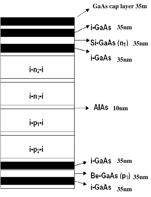
LT-GaAs superlattice samples 27 Figure 3.6 Schematic illustration of the LT-GaAs structure containing six active regions (i-n1-i,
i-n2-i, i-n3-i, i-p1-i, i-p2-i, and i-p3-i multilayers). The “i” denotes 35 nm thick
undoped GaAs layer, “n1”, “n2”, and “n3” (“p1”, “p2”, and “p3”) denote the Si-doped
(Be-doped) GaAs layers with doping concentration of 1016, 1017, and 1018cm-3, respectively. A 10 nm AlAs layer separated each active region. 30 Figure 3.7 Schematic diagram of the LT-(Ga, Mn)As structure 33 Figure 3.8 RHEED intensity oscillation of the reflected beam during MBE growth of GaAs
38
Figure 3.9 Cross-sectional samples preparation for transmission electron microscopy 40 Figure 3.10 Schematic diagram to show TEM method to determine the number density
Figure 4.1(c) Cross-sectional TEM bright-field images of Sample H3 (The annealed LT-GaAs on GaAs(311)B substrate) 50 Figure 4.2(a) Plan-view TEM images of Sample H1 (The annealed LT-GaAs on GaAs(001)
substrate) 51
Figure 4.2(b) Plan-view TEM images of Sample H2 (The annealed LT-GaAs on GaAs(311)A
substrate) 52
Figure 4.2(c) Plan-view TEM images of Sample H3 (The annealed LT-GaAs on GaAs(311)B
substrate) 53
Figure 4.3 DXRD rocking curves of as-grown LT-GaAs of Samples H4, H5, and H6: (004) reflection for sample grown on (001), (311) reflections for samples grown on (311)B and (311)A substrates 54 Figure 4.4 Schematic illustration of ideal atomic structures at (311)A and (311)B surfaces
55
Figure 4.5(a) TEM bright field images of Sample B1 showing arsenic precipitates in different active regions after annealing at 600°C 58 Figure 4.5(b) TEM bright field images of Sample B2 showing arsenic precipitates in different
active regions after annealing at 700°C 59 Figure 4.5(c) TEM bright field images of Sample B3 showing arsenic precipitates in different
active regions after annealing at 800°C 60 Figure 4.6 DXRD rocking curves of GaAs (004) for 1-μm-thick undoped (Sample B6), [Si] =
1018 cm-3 doped (Sample B4), and [Be] = 1018 cm-3 doped (Sample B5) LT-GaAs
samples 61
Figure 4.7 Arsenic cluster number density in each i-x-i region after annealing at 700°C (Sample B2) and 800°C (Sample B3), where x = n or pi i 62
Figure 4.8 M-H curves of (Ga, Mn)As DMS (Sample C1) measured with in-plane magnetic field applied along [110] or [1−10] directions at 10K 65 Figure 4.9 M-T curves of as-grown and post-annealed (Ga, Mn)As DMS (Samples C1, C2
and C3) measured under 1 Oe in-plane magnetic field 66 Figure 4.10 Curie temperature values (TC) vs. thickness of as-grown and post-annealed (Ga,
Mn)As DMS (Samples C1, C2 and C3) 67 Figure 4.11 The DXRD rocking curves of as-grown and post-annealed (Ga, Mn)As DMS
respectively, at 10K 69 Figure 4.12(b) M-H curves of post-annealed sample C1 measured with in-plane magnetic
field applied along [110], [1−10], [100], [010] directions, respectively, at 10K 70 Figure 4.13(a) M-T curves of as-grown and post-annealed (Ga, Mn)As DMS (Samples D1),
with Ga0.93Mn0.07As epi-layer on (001) oriented substrate, measured under 1 Oe
in-plane magnetic field 73 Figure 4.13(b) M-T curves of as-grown and post-annealed (Ga, Mn)As DMS (Samples D2),
with Ga0.93Mn0.07As epi-layer on (311)A oriented substrate, measured under 1 Oe
in-plane magnetic field 74 Figure 4.14(a) M-H curves of Ga0.93Mn0.07As epi-layer on GaAs(001) oriented substrate
(Sample D1), measured with in-plane magnetic field applied along [110], ]
directions at 10K 75
] 10 1 [−
Figure 4.14(b) M-H curves of Ga0.93Mn0.07As epi-layer on GaAs(311)A oriented substrate
(Sample D2), measured with in-plane magnetic field applied along ,
directions at 10K 76
] 1 01
[ − [2−33] Figure 4.15 The DXRD rocking curves of as-grown and post-annealed (Ga, Mn)As DMS
(Sample D3) 77
Figure 4.16 The interfacial micrographs between (In, Al, Mn)As and InAlAs (Sample E4): (a) bright field TEM image and (b) lattice image 80 Figure 4.17 The DXRD rocking curves of (004) for (In, Al, Mn)As on InP (Sample E2, E4,
and E5) 81
Figure 4.18 The M-H curves for (In0.52Al0.48)0.95Mn0.05As epilayer on InP (Sample E2),
measured with in-plane magnetic field at 5K. Closed circles stand for “net” magnetization after subtracting the magnetization of InP substrate and solid line is results of linear fit of the experimental data. Inset shows the applied field dependence of magnetization at 5K for (In0.52Al0.48)0.95Mn0.05As epilayer on InP
(Sample E2) and “bare” InP substrate with same size 82 Figure 4.19. M-H curves of as-grown and post-annealed for (In Al ) Mn As epilayer
Figure 4.21 The DXRD rocking curves of (In1-yAly)1-xMnxAs epilayer on InP substrate
(Samples G1, G2, and G4) 88 Figure 4.22 (a) High-resolution lattice image of the In0.52Al0.48)0.89Mn0.11As/In0.52Al0.48As
interface region (Sample G3) and (b) the selected area diffraction pattern of (In0.52Al0.48)0.89Mn0.11As layer along [110] zone axis 89
Figure 4.23 M-H curves for (In1-yAl )y 1-xMnxAs on InP substrate (Sample G1, G2, G4, and G5)
with in-plane magnetic field applied along the direction. The dash dot line is a linear fit of the M-H curve for Sample G1 90
] 10 1 [−
Figure 4.24 M-T curves under 100 Oe in-plane applied magnetic field along with direction for (In
] 10 1 [−
1-yAly)1-xMnxAs on InP substrate (Samples G2, G3, G4, and G5)
CHAPTER 1
INTRODUCTION
III-V compound semiconductors are widely used for high-speed electronic devices as well as for optoelectronic devices. However the device size is getting smaller, the quantum effect will emerge as the size of device reducing to nanometer range. Thus, new materials of device, e.g. combined with the advantage of charges and spin of electrons, have been speculating by scientists. Conventional semiconductor device relies on electrical charge, while another important property of the electron spin plays no role in information communication and processing. A new class of devices based on the electron spin, rather than on the electrical charge, may yield the next generation of microelectronics. To combine semiconductors with magnetic materials, getting the advantage of charges and spin of carriers will create new device configurations. For instance, spintronics microprocessor could combine storage, logic, and computation on a single chip.
From a materials science point of view, the search for new magnetic semiconductors as well as some spintronic materials is making the field of spintronics more practical. III-V diluted magnetic semiconductors (DMS) are formed by incorporating magnetic atoms such as Mn into conventional semiconductors. Usually GaAs was grown at 600°C and InP at 450°C by MBE. The second phase (NiAs-structure MnAs) will be formed when Mn content is too high, which will interrupt the conductivity of materials. The LT-MBE has been developed; increase the Mn concentrations and suppress the segregation of second phase, thus III-V DMS is produced [Munekata-89-1849; Ohno-96-363]. In this thesis, the growth and
Spintronics
are utilized at the same time.
Charge
(
+
, )
( , )
Spin
For the application of magnetic semiconductors, a Curie point for ferromagnetic above room temperature is required. Zener model of ferromagnetism proposed by Dietl et al.
[Dietl-00-1019] predicts that T
C = Cxp1/3, where x is the mole fraction of substitutional Mn+2 ions,
p is the concentration of hole and C is a constant specific to the host material. The growth substrate temperature (TS) of LT-MBE is around 200~300°C. Either TS or Mn content is too
high the second-phase (NiAs-structure MnAs) formation at the growth front would take place. The RHEED patterns during growth provide the in-situ check of whether the two-dimensional growth is retained. The maximum x obtained so far is 0.08–0.1, and beyond this critical concentration formation of second phase takes place even at low growth temperatures. While ordinary GaAs is grown at 600°C, low temperature growth results in structural disorder, including a high density of donor-like arsenic antisite (AsGa) and
interstitial Mn defects (MnI), which compensate the hole concentration. The concentration of
holes in the layer is only a fraction of the expected one, leading the degradation of magnetic and electrical properties [Yu-02-201303; Blinowski-03-121204].Currently, the value of Tc of (Ga,Mn)As
as high as 150-170K has been reported by several groups [Edmonds-02-4991; Ku-03-2302; Chiba-03-3020],
including the work presented in this thesis.
The recent discovery of ferromagnetism in III-V DMSs [Munekata. 89-1849; Ohno. 96-363] opens up the possibilities of real practical spintronic devices because of the maturity of III-V semiconductor technology. The research for new magnetic semiconductors and other suitable spintronic materials is bringing the field of spintronics closer to the realm of practice. The LT-MBE is the first motivating factor to perform these studies. It is essential to understand the inevitably excess arsenic on the epi-layer during LT-growth and its application for
postgrowth annealing. Nevertheless, control of the density and distribution of arsenic precipitates is crucial for potential device applications. The aim of the study is to study effects of substrate orientation, doping type and concentrations on arsenic precipitation.The arsenic precipitation behavior was carefully characterized by transmission electron microscopy (TEM) and discussed.
(2) Structure and magnetic property of LT-(Ga, Mn)As DMS on GaAs wafers
(Ga, Mn)As growth on substrates with different (001) or (311)A orientations have an influence on the magnetic properties of this material. The extensive research activity in this field caused considerable progresses in understanding the physical phenomena leading to integrated ferromagnetism in III-V DMS. The aim of the study is to study structures and magnetic properties of the (Ga, Mn)As epitaxial films on GaAs substrates, focusing on effects of different orientation substrates, thickness and post-annealing on the magnetic properties of Ga0.93Mn0.07As, where high concentration Mn content exists.
(3) Magnetic property of the layer structures of LT-(In, Al, Mn)As DMS with LT-(In, Al)As buffers on InP wafers
It is well-known that most of III-V DMS are ternary and grown on GaAs substrates. Demonstrating the magnetic properties of new quaternary DMS, e.g. (In, Ga, Mn)As and (In, Al, Mn)As grown on InP substrates is significant for the study of spin transport effects in devices built on InP substrates. Moreover, such quaternary magnetic semiconductor has many potential advantages, for example, it is easy to adjust the bandgap energy, easy magnetization direction, and band structure by changing the indium content, which cannot be realized by ternary alloy magnetic semiconductors. Also, the quaternary (In, Al)1-xMnxAs
DMS raises the possibility of fabricating complex heterostructures with engineered properties, combining magnetic layers having a large variety of electronic, optical, and spintronic
project is to studystructures and magnetic properties of the (In, Al, Mn)As epitaxial films on
InP substrates, series of quaternary DMS, (In0.52Al0.48)1-xMnxAs and (In1-yAly)1-xMnxAs
CHAPTER 2
TECHNICAL BACKGROUND
2.1 Structures, properties and applications of GaAs and InP
III-V compound semiconductors such as GaAs, InP crystalline is cubic zinc-blende structure, which consists of two interpenetrating fcc sublattices. One sublattice is displaced by 1/4 of a lattice parameter in each direction from the other sublattice, so that each site of one sublattice is tetrahedrally coordinated with sites from the other sublattice. Figure 2.1 shows a unit cell of zinc-blende structure.
Ga
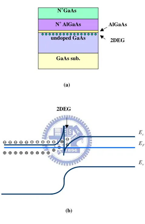
The benefit of GaAs over Si is its application to communications industry. GaAs is a kind of direct band gap material with the ability to emit light, which is useful for making lasers, light-emitting diodes, and microwave emitters used in cellular phones. Besides, it is attractive for high-speed devices since the electron saturation velocity in GaAs is 1.5 times that of Si. Scientists have been intrigued with the idea of fabricating artificial structures. The heteroepitaxial techniques allow one to grow heterostructures by changing the periodicity of the crystal during growth. The most widely used heterostructures are quantum wells, in which a single layer of one semiconductor is sandwiched between two layers of a large bandgap material. Such structures allow one to exploit special quantum effects that have become very useful in electronic and optoelectronic devices. The major application of GaAs at present is in the areas of microwave devices, high-speed digital integrated circuit, and as substrates for epitaxial layer growth to fabricate photonic and electronic devices. Figure 2.2(a) Shows schematic diagram of high electron mobility transistor (HEMT) with a junction between two materials with different band gaps e.g. GaAs and AlGaAs. The effect of this junction is to create a very thin layer where the Fermi level is above the conduction band, giving the channel very low resistance. This layer is called a two-dimensional electron gas(2DEG). A voltage applied to the gate alters the conductivity of this layer. Figure 2.2(b) Shows schematic diagram of 2DEG be formed at the heterojunctions.
For InP, the use is almost exclusively as substrates for growing lattice matched epitaxial film of alloy semiconductors such as In0.53Ga0.47As and In0.52Al0.48As, the heterostructure
epitaxy films can be formed on InP substrates. These ternary compounds semiconductor has many potential advantages, for example, it is easy to adjust the bandgap energy and band
GaAs sub. AlGaAs undoped GaAs N+ AlGaAs N+GaAs 2DEG (a) v E c E F E 2DEG (b)
Figure 2.2(a) Schematic diagram of HEMT, (b) schematic diagram of 2DEG at the heterojunctions
2.2 III-V diluted magnetic semiconductors (DMS)
The III-V semiconductors such as GaAs have been in use in a wide variety of electronic equipments in the form of electronic and optoelectronic devices. Recently, III–V diluted magnetic semiconductors (DMSs), e.g. (In, Mn)As and (Ga, Mn)As have attracted intense attention due to their significance in basic physics and potential application to spintronics devices [Ohno. 92-2664; Hayashi. 97-4865]. Since the hole-mediated ferromagnetism [Dietl. 00-1019] in III–V semiconductors is sensitive to both electrical and less understood structural properties, the investigation of new diluted magnetic semiconductor is interesting and rewarding [Hayashi.
01-169139; Ohya. 03-139; Matsukura. 02-1].
The first successful growth of (In,Mn)As thin film on GaAs substrates was reported by Munekata et al. in 1989 [Munekata. 89-1849]. Subsequent discovery of the hole-induced ferromagnetism in p-type (Ga,Mn)As by Ohno et al. in 1996 [Ohno. 96-363]. The properties of (Ga,Mn)As films in relation to the growth parameters [Ohno. 98-363; Shen. 99-679]have been reported. Typical (Ga,Mn)As is realized by using solid source MBE where in Mn provides both localized spin and holes. Mn atoms couple to charge carriers in the host semiconductors via the exchange interaction, and the carriers behave like connectors, which get spin information from one Mn atom and deliver to the other Mn atoms. The spin of Mn atoms can be aligned in the same direction so that the (Ga, Mn)As compound exhibits ferromagnetic state. Figure 2.3 shows schematic diagram of carrier-induced ferromagnetism.
The lattice constants of LT-(Ga,Mn)As DMS were reported by a few investigators [Ohno.
96-363; Sadowski. 01-3271], which were determined by DXRD techniques. It was found that the
lattice constant of LT-(Ga, Mn)As increases linearly with increasing Mn content. Basing on Vegard’s law, the lattice constant (a) at room temperature for (Ga1, Mn)As DMS can be
expressed by the following relations[Ohno. 96-363, Sadowski. 01-3271]
a = 0.566(1-x) + 0.598x (nm) (2-1) and a = 0.5654(1-x) + 0.5901x (nm) (2-2) where x is fraction of Mn content, and the relation is a function of BEP and substrate temperature. Where BEP denotes beam equivalent pressure.
Usually, magnetic measurement of (Ga, Mn)As is carried out in a superconducting quantum interference device (SQUID) magnetometer. Ohno et. al. reported that the magnetization of easy axis of (Ga, Mn)As dependent on the strain of epilayers [Ohno. 96-405]. The direction of the magnetization of easy axis is in perpendicular to surface of (Ga,Mn)As with tensile strain on a thick lattice-relaxed (In0.16Ga0.84)As buffer layer, while for (Ga,Mn)As on a GaAs buffer layer
with compressive strain, the direction of the magnetization of easy axis is in-plane.
Prinz et al. have reported a concept of spin valve [Prinz. 98-1660]. Figure 2.4 shows schematic diagrams of a spin valve. Two ferromagnetic layers were considered, a sandwiching non-magnetic conducting layer between them, which can function as either a conductor, or an insulator, for electrons. This means that the spin valve acts as a conductor for parallel of spin electrons, while it behaves as an insulator for anti-parallel spin electrons of two ferromagnetic layers. In Figure 2.4 (a), the device is expected as a conductor and the resistance is at its minimum, (b) the device is expected as an insulator. Thus, the resistance of this device strongly depends on the relative configurations of the ferromagnetic moments. This simple tri-layer system is commonly referred as a “spin valve”. For practical usage, it is often
to reverse.
(a) Conductor
(b) Insulator
Figure 2.4 Schematic diagram of a spin valve, a material can function as either (a) a conductoror (b) an insulator for electrons
Both giant magnetoresistance (GMR) and tunneling magnetoresistance (TMR) are attracting much attention because of their potential applications in magnetic recording technology and memory devices. GMR effect is due to the spin-dependent scattering in metallic multilayers and TMR effect is due to the spin-dependent tunneling in ferromagnet/insulator/ferromagnet tunnel junctions. TMR effect, have been reported by Higo’s group [Higo. 01-292]. The
light-emitting spintronic devices using III-V heterostructures on GaAs substrate have been reported by Ohno’s group [Ohno-99-709]. Their experimental results exhibiting the potentialof ferromagnetic semiconductors based on III-V compound semiconductors system for exploring new physics and fordeveloping new functionality toward future electronics.Other advantages of the new spintronic devices include increased data processing speed, decreased electric power consumption, and increased integration densities compared to semiconductor devices [Wolf. 03-703]. For instance, magnetic random access memory (MRAM) has the potential to higher data storage, faster data access and less power consumption than conventional memory devices. However, the Tc values to be expected by the mean-filed Zener model
[Dietl-02-1019] as if of 5% Mn and 3.5×1020 cm-3 of holes are introduced into wide-gap
semiconductors, the materials will be ferromagnetic at room temperature. As for Ga1-xMnxAs
semiconductors, if the hole density of p is 3.5x10²⁰ ㎝-3, it will be possible to achieve a Tc
beyond room temperature by increasing the Mn density to x =0.15. Figure 2.7 a Curie temperature was expected by the mean-filed Zener model [Dietl 00-1019].
Recently, Tc increases to 160–170 K [Edmonds-02-4991; Ku-03-2302]. Mathieu et al.
Mathieu-03-184421] and Sørensen et al. [Sørensen-03-2287] studied the thickness dependence of
magnetic properties for ultrathin Ga1-xMnxAs (≤ 25 nm) and have been reported. Very
recently, several groups had focused on Mn doped (In, Ga)As and the Curie temperature of 100–130 K, similar to that of (Ga, Mn)As, had been reported in (In, Ga) Mn As with x ≥
2.3 LT-MBE
While ordinary GaAs is grown at 600°C, GaAs grown at a low temperature (LT-GaAs) has attracted much attention due to its unique electronic and optical properties [Look-90-3578;
Nolte-93-1356]. When growing at 200 ~ 300°C, the GaAs layer contains quenched-in arsenic
(~1%) in excess of the bulk equilibrium concentration [Kaminska-89-1881]. This excess arsenic thus results in an expansion of the lattice and a high concentration of antisite defects with a deep-level donor-like character [Liliental-Weber- 91- 2153]. The reduced recombination time of approximately 400 fs [Gupta-91-3276] makes LT-GaAs very suitable for integrated subpicosecond optoelectronic switches [Loukakos-01-2883; Yano-03-3966]. Moreover, upon post-growth annealing above 500°C, excess arsenic precipitates into clusters, accompanied by the relaxation of strain, and the resistance of LT-GaAs changes from a low-resistivity state to an excellent semi-insulating state [Warren-90-1331]. The arsenic precipitates have been identified ashexagonal arsenic [Melloch-90-1531].
This semi-insulating property offers the benefits of excellent device isolation in GaAs The optically inactive, and crystalline, and high-quality GaAs active layers can be grown on top of the buffer to improve output resistance and breakdown voltages was reported [Smith-88-77]. And a metal-semiconductor field-effect transistor (MESFET) utilizing surface layers of GaAs grown at a low temperature by MBE (LT-GaAs) under the gate electrode has been reported. The high trap density of LT-GaAs reduces the surface fields of the FET, suppresses gate leakage, and increases the gate-drain breakdown voltage without sacrificing current drive capability [Lin-90-561].
the metallic arsenic precipitate forms a Schottky barriers at metallic/GaAs interface, depleting a portion of the surrounding apace. When the depletion regions are overlapped, the material will demonstrate the semi-insulating property.
Previous studies showed that arsenic precipitation in annealed LT materials can controlled by doping effects [Melloch-92-177; Liu-95-279; Missous-94-3396]. It has been found that arsenic
precipitates preferentially form in Si-doped GaAs then intrinsic and least favorably in Be-doped GaAs for moderately doped GaAs. However, when the Si and Be doping concentrations reach certain levels (≥ 5 x 1018 cm-3), an opposite precipitation behavior occurs
[Huang-03-305; O’Hagan-96-8384] and arsenic precipitation at the i/n interface will be influenced by the
Debye length λD. . ) ( 2 / 1 2 0 ⎥ ⎦ ⎤ ⎢ ⎣ ⎡ − = A D D N N q kT εε λ (2-3)
CHAPTER 3
EXPERIMENTAL METHODS
3.1 Flow chart of the experiments
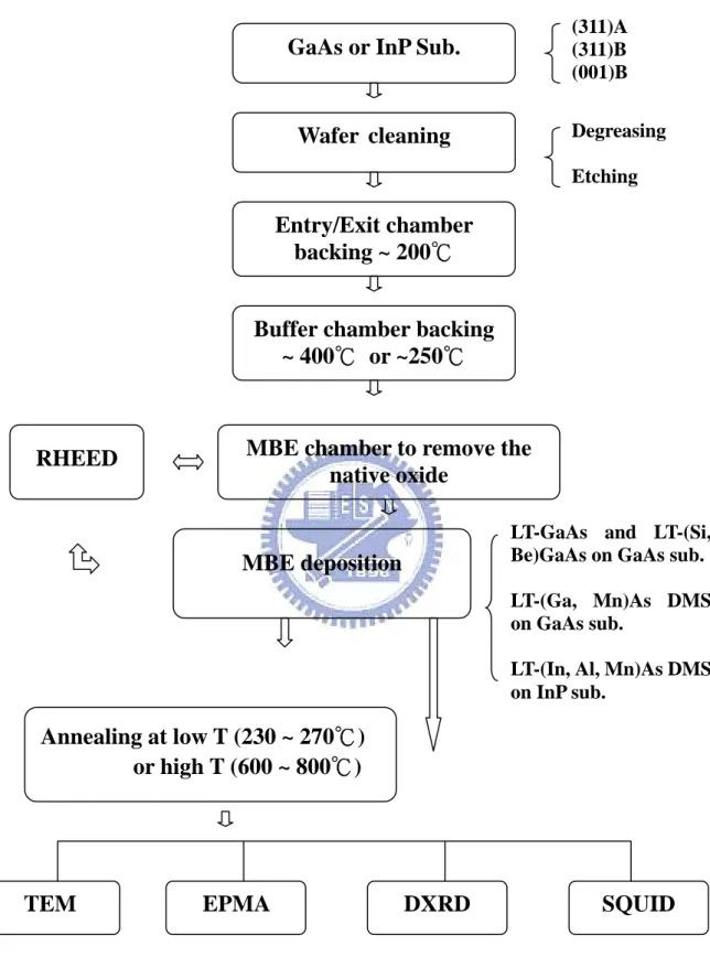
In this experiment, GaAs and InP wafers were used as the substrates to deposit LT-GaAs, LT-(Ga, Mn)As and LT-(In, Al, Mn)As by MBE system. The wafers were thoroughly degreased using organic solvents and then baked to remove the adsorb vapor. The baked samples were then transfer to the MBE growth chamber and subjected to de-oxidation to remove the oxides from the surface, and then followed by MBE deposition. The grown samples were examined by TEM, DXRD, EMPA and SQUID. The detailed procedures are shown in Figure 3.1.
Figure 3.1 Flow chart of the experiments
Annealing at low T (230 ~ 270℃)
or high T (600 ~ 800℃)
SQUID
DXRD
EPMA
TEM
Wafer cleaning
Entry/Exit chamber
backing ~ 200℃
GaAs or InP Sub.
(311)A (311)B (001)B
Degreasing Etching
Buffer chamber backing
~ 400℃ or ~250℃
MBE deposition
LT-GaAs and LT-(Si, Be)GaAs on GaAs sub. LT-(Ga, Mn)As DMS on GaAs sub.
LT-(In, Al, Mn)As DMS on InP sub.
MBE chamber to remove the
native oxide
3.2 MBE growth system
A MBE of Varian GEN-II ultra-high vacuum (UHV) system includes Entry/Exit chamber, buffer chamber, and growth chamber. ion pump, cryo-pump, titanium sublimation pump, dry pump, and sorption pumps are used to achieve UHV pressures in the chamber. Figure 3.2 shows a schematic diagram of MBE growth chamber system. The growth chamber includes 8 source cells (including two Ga sources, Al, In, Mn, Be, Si and arsenic sources), reflection high-energy electron diffraction (RHEED) analysis system, ionization gauges, quadruple mass spectrometer and rotating substrate holder. The working ranges of 5 different types of vacuum pumps in the systems are:
(1) Sorption pump: 760 ~ 10-4 torr (2) Dry pump: 760 ~ 10-6 torr (3) Ion pump: 10-3 ~ 10-11 torr
(4) Cryogenic pump: 10-3 ~ 10-10 torr
(5) Titanium sublimation pump: 10-4 ~ 10-11 torr
The growth chamber is equipped with 8 source cells configured in circle array, and the central axes of these cells cross at the substrate holder. The beam flux monitor is an ion gauge located 180° from the substrate. By rotating this ion gauge to the growth position, it is possible to measure the change in pressure caused by molecular beams striking the gauge. The molecular and atomic beams can be switched on and off by shutters in front of the cells, which are actuated by computer control. The Eurtherm controller governs the temperature of each substrate heater and all sources heated with a temperature accuracy of typically ±0.1℃.
Figure 3.2 Schematic diagram of MBE growth chamber system (From the Manual of Varian GEN-II, 1987)
3.3 Raw materials and wafer pretreatments
The raws materials used in this experiment include 7 different source materials for MBE deposition, two substrate materials (GaAs and InP) and some organic solvents and etching solutions. The specifications of the raw materials are shown in the following tables.
Source Purity Manufacturer
Gallium 8N Wafer Technology
United Mineral &Chemical corp Arsenic 7N
Manganese 7N Wafer Technology
Aluminium 6N UMAT
Indium 7N RASA Industries Silicon 7N Wafer Technology
Beryllium 5N Wafer Technology
Chemical solution Manufacturer
Acetone CMOS J. T. Baker Methanol CMOS J. T. Baker
Merck Hydrogen peroxide 31﹪ Merck Sulfuric Acid 98﹪ Merck Hydrochloric Acid 30﹪ Merck Ammonium Hydroxide 10﹪ Merck Bromine 15﹪ Substrate Manufacturer
GaAs(001) American Xtal Technology GaAs(311)A American Xtal Technology
Wafer pretreatment includes wafers cleaning, baking and deoxidization. The GaAs and InP wafers were used in this study. The cleaved wafers were first chemically cleaned and blown dry with nitrogen gas. Mount the wafers on Mo blocks for sample handling. Load and bake them in entry/exit chamber at 200℃ for 2 hour to desorb the water vapor, and followed by baking in buffer chamber at 400℃ for 30 min for GaAs wafers (or at 250℃ for InP wafers) for further outguessing the chemical organic solvent. The samples are then transferred to growth chamber and subjected to de-oxidation to remove the oxides from the surface. The de-oxidation process was monitored in situ with reflection high-energy electron diffraction (RHEED) system. When the surface protective oxide layer was removed, the surface reconstruction RHEED pattern changed to streak, as shown in Figure 3.3. The epi-layers structure was then grown.
The cleaning procedures for GaAs and InP substrates are different. The detailed procedures are described as below:
For GaAs wafers cleaning procedures:
(1) Degreasing steps: Sequence with hot acetone, methanol, and rinsed in deionized water.
(2) Etching steps: H2SO4 : H2O2 : H2O (5:1:1) for 10 minutes.
(3) After etching, the wafer is flooded with deionized water to stop the etchant, rinsed in deionized water, and blown dry with nitrogen gas.
For InP wafers cleaning procedures:
(1) Degreasing steps: Sequence with hot acetone, methanol, and rinsed in deionized water.
3.4 MBE system calibration
The system calibration for growth rate and doping concentration is essential to MBE precise deposition. One way to calibrate the growth rate is to use the BEP gauge. The BEP is proportional to the flux at the sample surface and hence the growth rate. This measurement is dependent on factors such as the geometry of the system and ionization efficiency of the material being measured. One way to calibrate the growth rate is to use the BEP gauge. The BEP is proportional to the flux at the sample surface and hence the growth rate. This measurement is dependent on factors such as the geometry of the system and ionization efficiency of the material being measured.
For calibration of growth rates (In, Al, Mn, Ga)
The furnace for growth are set to the intended operating temperatures, and allowed to equilbrate for about 20 minutes. It is easier to change the Group III fluxes rather than the Group V fluxes. For a given system, the relative flux ratios from two cells may be calculated from the beam equivalent pressures (BEP) values according to:
2 / 1 2 1 2 1 1 ( ) M T M T n n BEP BEP JJ =2 2 1 2 1 (3-1)
Where Jx: Beam flux, T: cell temperature (K), M: molecular weight and n: ionization
efficiency.
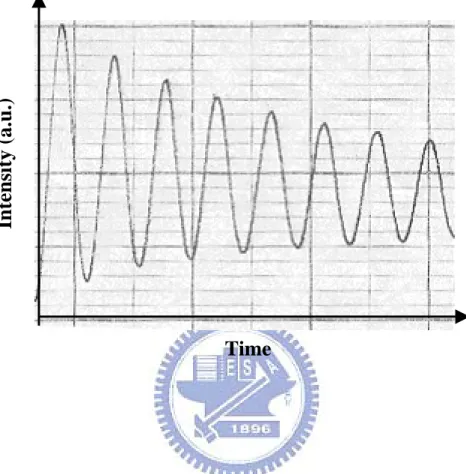
The growth rates were measured by RHEED oscillation at given furnace and substrate temperatures. During growth of a high quality surface oscillations in intensity of the integral streaks can be observed, which can in very simple terms be described by layer-by-layer growth, where a complete layer gives the brightest streaks, while a half layer somewhat disturbs the surface periodicity causing the RHEED intensity to decrease. The frequency of
periodically changes its morphology because of the nucleation and coalescence of islands in the growing layers.
For calibration of doping concentration (Si, Be)
Substiuting the dopent atoms of Si for Ga sites will form an n-type GaAs. And substiuting the dopent atoms of Be for Ga sites will form a p-type GaAs. The doping concentrations of as-grown samples measured by a C-V electrochemical system or a Hall set-up.
For calibration of Mn concentrations
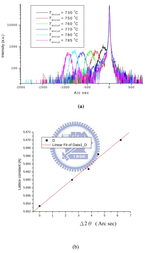
A relation of lattice constants versus Mn cell temperature was shown in Fig. 3.4(a) X-ray diffraction (XRD) measurements show that the (004) reflection of (Ga,Mn)As has the zinc-blende structure and the lattice constant a of (Ga,Mn)As increases with the increase of cell temperature (b) A relation of lattice constants of (Ga, Mn)As versus Mn content. Mn contents were determined by electron microprobe analysis (EMPA).
-2 0 0 0 -1 5 0 0 -1 0 0 0 - 5 0 0 0 5 0 0 1 0 0 1 0 0 0 1 0 0 0 0 In te n s it y (a .u .) A rc s e c TM n C e ll = 7 3 0 0C T M n C e ll = 7 5 0 0 C TM n C e ll = 7 6 0 0C T M n C e ll = 7 7 0 0 C TM n C e ll = 7 8 0 0C TM n C e ll = 7 8 5 0C (a) 0 1 2 3 4 5 6 7 5.652 5.654 5.656 5.658 5.660 5.662 5.664 5.666 5.668 5.670 5.672 D
Linear Fit of Data1_D
L a tt ic e const a nt (A) Mn (%)
Δ2θ ( Arc sec) (b)
Figure 3.4 The surface reconstruction (a) Double crystal X-ray diffraction (DXRD) measurements show that the (004) reflection of (Ga,Mn)As has the zinc-blende structure
3.5 Growth of LT-GaAs and LT-(Si,Be)GaAs on GaAs wafers
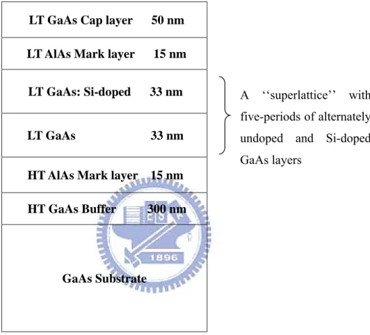
This experiment includes two parts, (1) the effects of substrate orientation and (2) the effects of doping type and concentrations on arsenic precipitation.The growth procedures for the 1st part are as follow: The sample designations and their growing conditions for different structures are shown in Table 3.1 and Figure. 3.5. The epi-layers of LT-GaAs were grown on (001), (311)A, and (311)B GaAs substrates, denoted as H1, H2 and H3. Growth rates of 0.8 μm/h for GaAs and 0.2 μm/h for AlAs and and V/III beam equivalent pressure ratio of 15 were used. The LT-GaAsstructure consists of a 5-period ‘‘superlattice’’ of alternately undoped and [Si] = 3 × 1018 cm-3-doped GaAs layers. The three (001), (311)A, and (311)B GaAs substrates were mounted on the same Mo block to ensure identical growth conditions. Following native oxide desorption, a 300 nm undoped GaAs buffer layer was first grown at 580°C to smooth the surface, followed by a 15 nm AlAs mark layer at the same temperature. Growth was then interrupted and the substrate temperature was ramped down to 250°C. The 5 periods of 33 nm undoped and 33 nm Si-doped GaAs ‘‘superlattices’’, a 15 nm AlAs diffusion barrier, and a 50 nm GaAs cap layer were subsequently grown. The AlAs layer was grown as a marker for later transmission electron microscope observations. Post-growth annealing was carried out by a rapid thermal annealing system at 800°C in forming gas for 30 s. To further characterize the concentration of excess arsenic incorporated into the LT-GaAs layers, three samples with 1000 nm undoped LT-GaAs were also grown under the same growth conditions as aforementioned on the (001), (311)A, and (311)B-oriented substrates, denoted as H4, H5 and H6.
Table 3.1
Sample designations and their growing conditions of the LT-GaAs and LT-(Si, Be)GaAs epi-layers structures
Sample
No. BEP (V/III)
※
*Growth rates of GaAs = 0.8 μm/h; AlAs = 0.2 μm/h Substrate temperature = 250℃
△
For samples H1~H6: BEP of Ga = 7x10⁻⁷ torr, BEP of As = 1.05x 10⁻⁵ torr For samples B1~B6: BEP of Ga = 7x10⁻⁷ torr, BEP of As = 1.75x 10⁻⁵ torr
Substrate △
ratio Epi-layer structure* Post-annealing(Thickness, nm) (℃) GaAs(001) H1 15 as Fig.3.4 800 GaAs(311)A H2 15 as Fig.3.4 800 GaAs(311)B H3 15 as Fig.3.4 800 LT-GaAs H4 GaAs(001) 15 x (1000) LT-GaAs H5 GaAs(311)A 15 x (1000) LT-GaAs H6 GaAs(311)B 15 x (1000) GaAs(001) B1 25 as Fig.3.5 600 GaAs(001) B2 25 as Fig.3.5 700 GaAs(001) B3 25 as Fig.3.5 800 LT-Si-doped GaAs (1000) B4 GaAs(001) 25 x LT-Be-doped GaAs (1000) B5 GaAs(001) 25 x Undoped LT-GaAs B6 GaAs(001) 25 x (1000)
LT GaAs Cap layer 50 nm
LT AlAs Mark layer 15 nm
LT GaAs: Si-doped 33 nm
Figure 3.5 the surface reconstruction Schematic structures of alternately undoped
LT GaAs 33 nm
HT AlAs Mark layer 15 nm
HT GaAs Buffer 300 nm
GaAs Substrate
A ‘‘superlattice’’ with five-periods of alternately undoped and Si-doped GaAs layers
The growth procedures for 2nd part on the effects of doping type and concentrations on arsenic precipitation are shown in Table 3.1 and Figure 3.6. Previous studies showed that arsenic precipitation in annealed LT materials be controlled by doping effects, It has been found that arsenic precipitates preferentially form in Si-doped GaAs than intrinsic and less favorably in Be-doped GaAs for moderately doped GaAs. However, when the Si and Be doping concentrations reach certain levels (≥ 5 x 1018 cm-3), an opposite precipitation behavior occurs [Huang-03-305]. Both the inter-diffusion of arsenic related defects and doping effects during annealing among the LT layers make this a more complicated system for understanding the arsenic precipitation behavior in lightly doped LT-GaAs. Thereby, the aim of the project is to study effects of doping type and concentration on arsenic precipitation.
The designed structure consists of three i-n-i and three i-p-i active regions, with doping levels ranging from 1016 to 1018 cm−3, in which each active region is separated with a 10 nm AlAs marker layer. Owing to the high activation energy but small diffusion constant for Al and Ga inter-diffusion,the thin AlAs layer acts as an inter-diffusion barrier between adjacent active regions, and the effects of doping type and concentration on arsenic precipitation behaviors can be clearly recognized. The growth rates of 0.8 μm/h for GaAs and 0.2 μm/h for AlAs and the V/III beam equivalent pressure ratio of 25 were used. Following native oxide desorption, a 100 nm GaAs buffer layer was first grown at 580°C to smooth the surface, followed by a 10 nm AlAs diffusion barrier at the same temperature. Growth was then interrupted by closing the Al effusion furnace shutter, the substrate temperature was ramped down to 250 °C and the As shutter was closed when the substrate temperature was below 400 °C to maintain a clear 2x4 surface reconstruction, as observed by reflection high-energy electron diffraction (RHEED). It took about 15 minutes to stabilize the substrate temperature. Subsequently, the low-temperature active layers and a 35 nm GaAs cap layer were grown. The
undoped/Si-doped/undoped (i-n-i) multilayers. Each i-n-i or i-p-i region was separated by a thin AlAs layer, which acted as both a diffusion barrier and a marker layer. The thickness of each doped or undoped GaAs layer was 35 nm. The doping levels in the p1, p2 and p3 layers
(and n1, n2, and n3 layers) were 2 x 10¹⁶, 2 x 10¹⁷, and 2 x 1018cm-3, respectively.
The as-grown the sample was cleaved into three pieces and the post-annealing was carried out in a rapid thermal annealing (RTA) system at 600, 700 and 800°C for 30 s, respectively, denoted as B1, B2 and B3. To further characterize the concentration of excess As incorporated into the LT-GaAs layers, three 1 μm thick LT GaAs samples of [Si] = 1018 cm-3 doped, [Be] = 1018 cm-3 doped and undoped were also grown under the same growth conditions as aforementioned, denoted as B4, B5 and B6.
GaAs cap layer 35m
35nm
35nm
35nm
10nm
35nm
35nm
35nm
Figure 3.6 Schematic diagram of the LT-GaAs structure containing six active regions (i-n1-i, i-n -i, i-n -i, i-p -i, i-p -i, and i-p2 3 1 2 3-i multilayers). The “i” denotes 35 nm thick
undoped GaAs layer, “n ”, “n1 2”, and “n ” (“p ”, “p3 1 2”, and “p3”) denote the Si-doped
3.6 Growth and post annealing of LT- (Ga, Mn)As DMS on GaAs wafers
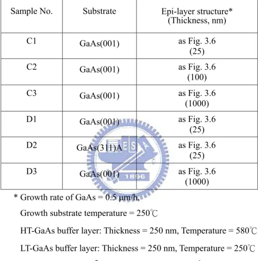
This experiment includes two parts, (1) the effects of thickness and post-annealing and (2) the effects of substrates orientation on the magnetic properties of Ga0.93Mn0.07As. The
growth procedures for the 1st part are as follows: The sample designations and their growing conditions for different structures are shown in Table 3.2 and Figure. 3.7. The Samples of (Ga, Mn)As DMS on GaAs wafers were grown on GaAs (001) substrates. A growth rate of 0.5 μm/h and a V/III beam equivalent pressure ratio of 15 were used. Following native oxide desorption, a 250 nm thick GaAs buffer layer was first grown at 560°C to smoothen the surface. Then the substrate temperature was lowered to 250°C, and subsequently 250 nm LT-GaAs buffer layer was grown. Finally, a series of 25 nm, 100 nm and 1000 nm of Ga0.93Mn0.07As epi-layers were grown, respectively, denoted as C1, C2 and C3. Post-growth
annealing of samples are carried out at 250℃ for 1.5 hrs in air.
The growth procedures for the 2nd part of the effects of substrates orientation on the magnetic properties of Ga0.93Mn0.07As are as follows: The sample designations and their
growing conditions for different structures are shown in Table 3.2 and Figure. 3.7. The samples of LT-(Ga, Mn)As DMS on GaAs wafers were grown on GaAs (001) and (311)A substrates, denoted as D1 and D2. The (001) and (311)A GaAs substrates were mounted on the same Mo block to ensure identical growth conditions. Growth rates of 0.5 μm/h for GaAs and a V/III beam equivalent pressure ratio of 15 were used. Following native oxide desorption, a 250 nm thick GaAs buffer layer was first grown at 580 °C to smoothen the surface. Growth was then interrupted and the substrate temperature was lowered to 250 °C,
Ga0.93Mn0.07As was subsequently grown on the (001) oriented substrates under the same
growth condition as aforementioned, denoted as D3.
Table 3.2 Sample designations and their growing conditions of the Ga0.93Mn0.07As
epi-layers structures
Sample No. Substrate Epi-layer structure* (Thickness, nm) C1 GaAs(001) as Fig. 3.6 (25) C2 GaAs(001) as Fig. 3.6 (100) C3 GaAs(001) as Fig. 3.6 (1000) D1 GaAs(001) as Fig. 3.6 (25) D2 GaAs(311)A as Fig. 3.6 (25) D3 GaAs(001) as Fig. 3.6 (1000) * Growth rate of GaAs = 0.5 μm/h,
Growth substrate temperature = 250℃
HT-GaAs buffer layer: Thickness = 250 nm, Temperature = 580℃ LT-GaAs buffer layer: Thickness = 250 nm, Temperature = 250℃ BEP of Ga = 4.5x10⁻⁷ torr, BEP of As = 6.75x 10 torr -6
HT-GaAs 250 nm (580℃) GaAs Substrate LT-GaAs 250 nm (250℃) LT-Ga0.93Mn0.07As (250℃)
25 ~ 1000 nm
3.7 Growth of LT-(In, Al, Mn)As DMS and LT-(In, Al)As buffers on InP
wafers
This experiment includes two parts, (1) (In0.52Al0.48)1-xMnxAs DMS and (2)
(In1-yAly)1-xMnxAs DMS. The growth procedures for the 1st part are as follows: The sample
designations and their growing conditions for different structures are shown in Table 3.3. A series of (In0.52Al0.48)1-xMnxAs / In0.52Al0.48As / InP layer structures were grown on (001)
semi-insulating InP substrates. The Samples are denoted as E1, E2, E3, E4 and E5. A growth rate of 0.3 μm/hr and a V/III beam equivalent pressure ratio of 20 were used. Following native oxide desorption, a 100 nm In0.52Al0.48As buffer layer was first grown at 460 °C to
smoothen the surface. Then, the substrate temperature was lowered to 220-230°C. Subsequently, the 100-nm-thick (In0.52Al0.48)1-xMnxAs (0 < x ≤ 0.11) active epilayer was
grown.
The as-grown samples were cleaved into a number of pieces for various characterizations. The cleaved samples were examined by double-crystalline x-ray diffraction (DXRD) and transmission electron microscopy (TEM). The cross-sectional samples parallel to (110) plane were prepared by mechanical thinning and followed by Ar-ion milling for TEM observation. Mn concentrations were determined by electron microprobe analysis (EMPA). Magnetic measurements were carried out in a superconducting quantum interference device (SQUID) magnetometer.
Table 3.3
Sample designations and their growing conditions of the (In1-yAly)1-xMnxAs / (In1-yAly)As / InP epi-layers structures
Sample No.△ Buffer layer structure
(Thickness, nm) (Thickness, nm) Epi-layer structure* E1 In0.52Al0.48As (100) (In0.52Al0.48(100) )0.97Mn0.03As E2 In0.52Al0.48As (100) (In0.52Al0.48(100) )0.95Mn0.05As E3 In0.52Al0.48As (100) (In0.52Al0.48)0.94Mn0.06As (100) E4 In0.52Al0.48As (100) (In0.52Al0.48)0.92Mn0.08As (100) E5 In0.52Al0.48As (100) (In0.52Al0.48)0.89Mn0.11As (100) G1 In0.52Al0.48As (100) (In0.52Al0.48)0.95Mn0.05As (100) G2 In0.52Al0.48As (100) (In0.52Al0.48(100) )0.92Mn0.08As G3 In0.52Al0.48As (100) (In0.52Al0.48(100) )0.89Mn0.11As G4 In0.61Al0.39As (50)
In1-yAlyAs; 0.39<y<0.45
(75) In0.55Al0.45As (75) (In0.61Al0.39)0.85Mn0.15As (100) G5 In0.63Al0.37As (50)
In1-yAlyAs; 0.37<y<0.45
(75) In0.55Al0.45As (75) (In0.63Al0.37)0.82Mn0.18As (50) * Growth rate = 0.3 μm/h △
For Samples E1~E5 and G1~G3: BEP of Al = 3.0 x 10⁻⁸ torr, BEP of In =1.2 x 10⁻⁷ torr BEP of As = 3.0 x 10⁻⁶ torr
The growth procedures for the 2nd part are as follows: The sample designations and their growing conditions for different structures are shown in Table 3.3. A series of (In1-yAly)1-xMnxAs / (In1-yAly)As / InP layer structures were grown on (001) semi-insulating
InP substrates. The Samples are denoted as G1, G2, G3, G4 and G5. The samples of a growth rate of 0.3 μm/hr and a V/III beam equivalent pressure ratio of 20. Following native oxide desorption, a 100-nm In0.52Al0.48As or a graded 3-layer In1-yAlyAs buffer structure of 200 nm
thick was grown at 460 °C. Growth was then interrupted and the substrate temperature was lowered to 200-230 °C. Finally, a 50 or 100 nm (In1-yAly)1-xMnxAs epilayer of interest was
grown. Since the (In1-yAly)1-xMnxAs epilayers have larger lattice constants than the InP
substrate, here we have employed different (In, Al)As buffer layer structures, in order to avoid the misfit-induced dislocation and to obtain a smooth starting surface for the growth of (In1-yAly)1-xMnxAs epilayers. The surface reconstruction of the samples during growth was
monitored in situ with the reflection high-energy electron diffraction (RHEED). Basically, a (2x4) RHEED pattern was observed during the growth of high-temperature (In, Al)As buffer layers, while it changed to (1x1) or (1x2) during and after the growth of (In, Al, Mn)As layer, implying a two-dimensional growth mode. Had the Mn flux or the substrate temperature been too high, a complicated RHEED pattern would have appeared, implying the formation of a second phase on the sample surface [Park-05-396].
The as-grown samples were cleaved into pieces for various characterizations. The Mn concentrations were determined by a calibration curve based on the electron microprobe analysis (EMPA). The samples were examined by double-crystal x-ray diffraction (DXRD) and transmission electron microscopy JEOL JEM-2010 (TEM). Cross-sectional samples parallel to (110) plane were prepared conventionally by mechanical thinning and Ar-ion milling for TEM observation. Magnetic properties were measured by a Quantum Design
3.8 Structure analysis methods
(1) Reflection high-energy Electron Diffraction (RHEED)
The surface reconstruction of the samples during growth was monitored in situ with the reflection high-energy electron diffraction (RHEED) system. RHEED system employs an electron beam impinging on a sample at a grazing angle (typically about 1~2°) electron beam incidence is under Bragg diffraction condition of the surface. The diffracted beams can observe on a phosphorus screen. RHEED is a very powerful method for surface studies due to the fact that the electron beam penetrates only about 2 or 3 monolayers deep into the lattice, the reciprocal lattice will consists of lattice rods in the direction normal to the surface. When only elastic scattering events are considered, the diffraction condition can be cast into the geometrical construction of the Ewald sphere in reciprocal space. The Ewald sphere is much larger than the reciprocal rods of GaAs. This phenomenon produces an almost planar cut through the first few Brillouin zones of the reciprocal lattice. If a phosphorus screen is placed in a distance from the samples, diffraction spots on the screen to become streaks. Which is satisfied the Bragg condition of 2-D growth. An application of RHEED in MBE is to calibrate the growth rate. Figure 3.8 shows RHEED intensity oscillation of the reflected beam during MBE growth of GaAs; the period of oscillation corresponds precisely to a monolayer, ao/2 for GaAs. The period of the RHEED intensity oscillations is explicitly
related to the growth rate and as such is of practical value in determining the beam fluxes and in controlling the layer thickness accuracy to one monolayer.
Time
Intensity (a.u.)
Figure 3.8 RHEED intensity oscillation of the reflected beam during MBE growth of GaAs
(2) Transmission Electron Microscopy (TEM)
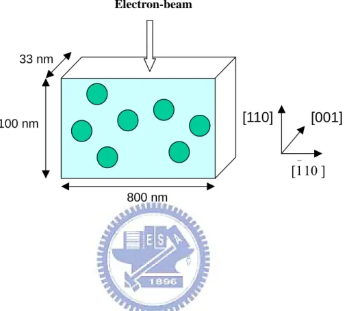
The morphology and crystallographic information of samples were characterized by transmission electron microscope (TEM). Transmission electron microscope uses a beam of high-energy electrons to project a magnified image of a sample onto a fluorescent screen. The size, number density and arrangement of the arsenic precipitation in the annealed LT-GaAs samples were examined using a JEOL JEM-2010 electron microscope. Cross-sectional samples for transmission electron microscopy observations were prepared with mechanical thinning and Ar-ion milling. Schematic illustration cross-sectional samples preparation procedures are shown in Figure 3.9(a)-(d). Figure 3.10 shows the number density of arsenic clusters for each sample is determined by assuming that the penetration thickness of electron beam of TEM is 100 nm. volume clusters of number average Density
=
The crystalline structures of (Ga, Mn)As and (In, Al, Mn)As epilayers were examined by transmission electron microscopy (TEM). Cross-sectional samples parallel to the (110) plane were prepared for TEM observation.
(a) The samples were cleaved into small rectangle pieces. Two rectangles were bonded face to face to for a stack, which then was glued on a glass plate.
(b) Mechanically thinning and polishing both top an
Figure 3.9 Cross-sectional samples preparation for transmission electron microscopy d bottom sides of the sample on a rotating wheel with running water to remove the scratches from the surface.
(c) After polishing, a copper ring was mounted with fast-drying cement. Then cut the excess thin film and place it in a small beaker with acetone until all glue was removed.
(d) The final step was Ar-ion milling to create electron transparent edges.
Electron-beam
Figure 3.10 Schematic diagram to show TEM method to determine the number density of arsenic clusters
33 nm 100 nm
[110]
[001]
800 nm]
10
1
[
−⊥
(3) Double-crystal X-ray Diffraction (DXRD)
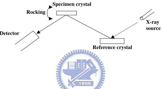
Information from substrate and epi-layer peaks includes lattice mismatch, composition, thickness and strain. The double-crystal diffractometer (DXRD) is a powerful characterization tool for epitaxial crystal growth. Samples can be easily mounted quickly and non-destructive evaluation of their materials parameters. Figure 3.11 schematically illustrates the top view of DXRD instrument, where the reference crystal is aligned to sit on the Cu Kα1 line and the
wavelength dispersion is eliminated by the reference crystal. And specimen crystals are provided with two rotation axes driven by stepper motors. The signals of rocking curves of samples are collected by the detector.
The Ga1-xMnxAs lattice constant is larger than that of GaAs, the corresponding
perpendicular lattice mismatches, (Δa/a) can be measured by DXRD. The (004) reflection of Ga1-xMnxAs epitaxial layers grown on (001) oriented GaAs substrates, the Bragg spacing is
given by a⊥/4 where a⊥ is the lattice parameter in the [001] direction. The mismatch of the
epitaxial layer is given by
B s s a a a a a θ θ tan ) (Δ = ⊥ − =− Δ ⊥ (3-2)
is the Bragg angle corresponding to a Here as is the lattice parameter of the substrate,θB s and
Δθis the measured angular separation between the Bragg peaks. The presence of two well-defined peaks indicates the existence of a single-crystal layer containing excess arsenic other than bulk GaAs in antisite and interstitial positions. The lattice expansion of the LT GaAs epilayer is directly proportional to excess arsenic content in the layer by double-crystal X-ray diffraction [Lavrent’eva-02-118]. Double-crystal X-ray diffraction (DXRD) rocking curves were examined using a Philip DCD-3 double-crystal diffractometer.
Reference crystal Specimen crystal
Figure 3.11 Schematic illustration of DXRD technique
X-ray source Rocking
3.9 Properties measurements
Superconducting Quantum Interference Device magnetometry (SQUID)
A Superconducting Quantum Interference Device (SQUID) uses the properties of electron-pair wave coherence and Josephson Junctions to detect very small magnetic fields. The MPMS5 system comprises of two main sections: the dewar, probe and SQUID assembly, and the electronic control system. The probe contains a high precision temperature control system, allowing measurements between 2 - 400K and superconducting electromagnet, giving a field of up to 5.5 Tesla.
The dewar consists of an inner liquid helium reservoir and outer liquid nitrogen jacket, to reduce excessive liquid helium boil off. The liquid helium is used for both maintaining the electromagnet in a superconducting state and for cooling the sample space. Samples are mounted within a plastic straw and connected to one end of a sample rod, which is inserted into the dewar/probe. The other end is attached to a stepper motor, which is used to position the sample within the center of the SQUID pickup coils. These measurements have a sensitivity of 5×10⁻⁸ E.M.U. To measure the magnetic properties of (Ga, Mn)As epi-layers, the sample is cooled down to 10K under an external field of 1000 Oe applied along the measurement axis. Then field is removed, and projection of the remnant magnetization along the measurement axis is recorded as a function of temperature.