國 立 交 通 大 學
光電工程研究所
碩
士
論
文
可應用於太陽能電池之奈米結晶矽量子點埋入式氧化鋅薄
膜之特性研究
Characteristics of the Nano-crystalline Si Quantum Dot
Embedded ZnO Thin Films for Solar Cell Applications
研 究 生:許書維
指導教授:李柏璁 博士
可應用於太陽能電池之奈米結晶矽量子點埋入式氧化鋅薄
膜之特性研究
Characteristics of the Nano-crystalline Si Quantum Dot
Embedded ZnO Thin Films for Solar Cell Applications
研 究 生:許書維 Student:Shu-Wei Hsu
指導教授:李柏璁 博士 Advisor:Dr. Po-Tsung Lee
國 立 交 通 大 學
光電工程研究所
碩 士 論 文
A Thesis
Submitted to Department of Photonic and Institute of Electro-Optical Engineering College of Electrical Engineering and Computer Science
National Chiao Tung University In partial Fulfillment of the Requirements
for the Degree of Master in
Department of Photonic and Electro-Optical Engineering July 2011
Hsinchu, Taiwan, Republic of China
I
可應用於太陽能電池之奈米結晶矽量子點埋入式氧化鋅薄
膜之特性研究
研究生:許書維
指導教授:李柏璁 博士
國立交通大學光電工程研究所碩士班
摘
要
目前在矽量子點太陽能電池的研究,其矽量子點皆埋入絕緣介質中,造成電 荷傳導上的不易,因而侷限住整體的光電轉換效率。因此在本篇論文,我們提出 利用氧化鋅來取代傳統的絕緣介質,因為它不但是半導體,易於電荷傳導外,更 具備其他特性,例如擁有大的能隙、高的穿透率、好的結晶性、以及易於調控的 電性等等,諸如以上優點,將奈米結晶矽量子點埋入氧化鋅材料中製作出的矽量 子點太陽能電池非常有發展潛力。 首先我們以磁控濺鍍機交替沉積氧化鋅與矽的多層膜,在第一部分以快速升 溫退火使矽量子點結晶,並利用來曼光譜與X光繞射圖譜分別確認奈米結晶矽量 子點的形成與氧化鋅薄膜的結晶品質,並分析其光電特性。我們發現在較高的矽 濺鍍功率下,矽原子擁有較高的表面移動動能,因此在沉積的過程便能自我聚集, 因而在後續的高溫退火下,易於形成奈米結晶矽量子點,並得到較佳的氧化鋅薄 膜結晶品質。第二部份改用爐管進行高溫退火使矽量子點結晶,是為了解決使用 快速升溫退火所產生的部分問題。而在爐管退火後我們可以得到不錯的整流比與 光響應。 最後一部分,我們就退火後薄膜產生很大的應力造成薄膜的剝離進行分析並 試圖找尋解決方法。我們發現利用升溫製程可望解決退火後因應力造成薄膜彎曲 的問題。II
Characteristics of the Nano-crystalline Si Quantum Dots
Embedded ZnO Thin Films for Solar Cell Applications
Student: Shu-Wei Hsu
Advisor: Dr. Po-Tsung Lee
Department of Photonics and Institute of Electro-Optical
Engineering, National Chiao Tung University
Abstract
The researches of Si quantum dot (QD) thin film solar cell are fabricated by using nanocrystal silicon (nc-Si) QDs embedded in the Si-based dielectric material. However the experimental results are still substantially lower than the theoretical value due to the unfavorable material characteristics of these Si-based matrices, that is, they are not electrically conductive. In this thesis, we propose to use Zinc oxide (ZnO) as the substitutable matrix material due to its many potential applications and unique features over other conventional wide band gap semiconductors such as high transparency, nice crystallinity, and easiness to control the electrical properties. Hence, ZnO is a suitable material to serve as the matrix for nano-crystalline Si quantum dot thin film solar cell.
We deposited ZnO/Si multilayer thin films by radio-magnetron sputtering. At first part, the nc-Si QD formed after annealing by rapid thermal annealing thermal process. We investigated the nc-Si formation and crystalline quality of the ZnO matrix by the analyses of Raman spectra and XRD patterns. Optical-electrical properties of the multilayer thin films after annealing are also investigated. We observe that the sputtered Si atoms have more kinetic energy to aggregate together as Si nano-clusters under higher Si sputtering power. An obvious aggregation of the sputtered Si atoms during deposition is helpful for the formation of nc-Si and the better crystallization of the ZnO matrix in the nc-Si embedded ZnO thin films during the RTA thermal process. At second part, we substitute RTA to furnace as our new thermal treatment equipment to solve some problems cause by RTA. And we observe good rectification ratio and better photon response after annealing by furnace.
At the last part, we try to solve the film bending problem cause by the high stress interior the films after annealing. We observe the film bending problem may be solved with a heated substrate during deposition.
III
Acknowledgements
驪歌響起,兩年來的碩班回憶就如旋律般縈繞心田。感覺有點不真實,但 一想到每個無理取鬧、搞笑逗趣、認真嚴謹的大小事,卻又是那麼樣的真實。不 管怎樣,隨著歌曲進入尾聲,我的碩士生涯也該畫下了休止符。 碩士求學的兩年來,我最最要感謝的是我的指導教授 李柏璁 博士,您是 位亦師亦友的好老師,不僅在研究上適時的給予學生很多寶貴建議,在排球場上 您更是最佳的先發,很感謝您的親切、您的好相處,還有我永遠會記得您年少時 期的瘋狂事蹟XD。再來要感謝帶領我的學長 光揚,感謝您對我自以為是、任性、 不受教的包容,當然還要感謝那台有牛奶味的筆電。在您的提點,指導下,這兩 年雖然辛苦但收穫卻比想像中多很多很多。一起奮鬥拼畢業的夥伴們 文齡、Ping, 妳們真的在實驗上幫我很多,讓我在做實驗的過程能事半功倍。已經畢業的學長 們胖胖、G龍、佑佑哥,不論在機台操作或問題討論上對我都有莫大的幫助,當 然還有夥伴雋崴、立勳、紹平,以及贊文、資岳、家揚、品佐、佳裕學長們,加 上權政、為智、哲嶢、開昊這群學弟妹們,你們每位大家都在我碩班生活裡扮演 不可或缺的角色,深深的一鞠躬,感謝PTLee這個大家庭。最後,感謝在碩班結 束前一起做thermal實驗的笨蛋,短短的一個半月,笨蛋事蹟卻可以講一年半之 久,我想我是開心的,謝謝你。 再來要感謝我的家人,我承認我不是個挺孝順的兒子,但你們卻還是無怨 無悔的給予支持,關心著不懂事的我,讓我可以恣意妄為的撒野,無憂無慮的放 縱,謝謝您們。但我還是要說,老爸,你兒子有朝一日一定會成為一位優秀的人。 最後,感謝交大,讓我在這裡遇到這麼多優秀的人,在這樣的環境下學習, 很棒、真的。未來十分令人期待,而我也整裝待發,揮灑,屬於我的人生。 許書維。2011 年7 月 謹誌於 新竹交通大學IV
Outline
Abstract (in Chinese)………I
Abstract (in English)……….……II
Acknowledgements……….……….III
Content……….………IV
List of Tables ………...VI
List of Figures ………....VII
Chapter 1 Introduction
1.1 Background………..1
1.2 Nano-crystalline Si Quantum Dots for Third Generation Solar
Cell……….………2
1.2.1 Concept of the Third Generation Solar Cell.………...2
1.2.2 Principles of Si Quantum Dot Thin Film Solar Cell…………...4
1.3 Paper Review………...5
1.3.1 Characteristics of ZnO Thin Film and ZnO/Si Hetrojunction
Solar Cell………...……….5
1.3.2 Silicon Quantum Dot Solar Cells………...……….……...6
1.4 Experimental Motivation………..………...10
Chapter 2 Sample Preparation and Analyses
2.1 Sample Preparation……….14
2.1.1 Substrate Clean……….14
2.1.2 Thin Film Deposition………15
2.1.3 Post Annealing Method……….…………...16
2.1.4 Electrode Deposition………...17
2.2 Sample Analyses…..………...18
2.2.1 Surface Morphology………..………...18
2.2.2 Structural properties………..………20
2.2.3 Crystalline property………..………21
2.2.4 Optical Property……...……….………23
2.2.5 Electrical P
roperty………..
………...24
V
Chapter 3 Experimental Results and Discussions
3.1 ZnO Thin Films………..………27
3.2 ZnO/Si Multilayer Thin Films with Rapid Thermal Annealing ……30
3.2.1 Structural Properties….……….30
3.2.2 Crystalline Properties of Nano-crystalline Si Quantum Dot….31
3.2.3 Crystalline Properties of ZnO Matrix………33
3.2.4 Influence of Surface Morphology………….………34
3.2.5 Electrical Properties………..……….36
3.2.6 Problems during Rapid Thermal Annealing Process………….39
3.3 ZnO/Si Multilayer Thin Films with Furnace Annealing Process...…40
3.3.1 Different Annealing Temperature……….41
3.3.2 Structural Properties……….….44
3.3.3 Crystalline Properties of Nano-crystalline Si Quantum Dot….44
3.3.4 Crystalline Properties of ZnO Matrix………..……….….46
3.2.5 Electrical Properties………..……….47
3.2.6 Problems during Furnace Annealing Process………49
3.4 Solutions for Film Bending Problem………..51
3.4.1 Decreasing the Pairs of Multilayer………52
3.4.2 Decreasing the Interior Stress Density of Multilayer………....53
3.4.3 Deposition with a Heated Substrate………..58
Chapter 4 Conclusion and Future Work
4.1 Conclusion………...60
VI
List of Tables
Table 1.1: 1-Sun illumination cell of four different n-type Si QDs/
p-type c-Si heteroface devices measured at 298K………….9
Table 2.1: Sputtering parameters of ZnO/Si single bilayer and
20-bilayers (ML) thin films. ……….15
Table 2.2: Post annealing parameters after deposition ...…16
Table 3.1: Four-point probe measurement of ZnO film under different
annealing conditions ………...29
Table 3.2: Parameters of multilayer thin films under different annealed
conditions…………..………...33
Table 3.3: Electrical properties of ZnO/Si multilayer thin films under
different P
si………...………38
Table 3.4: Parameters of sample S110 under different annealing
conditions………...…..42
Table 3.5: Electrical properties comparison of sample S110 between
different post annealing temperatures...………43
Table 3.6: Parameters of ZnO/Si multilayer thin films under different
P
si………..45
Table 3.7: Electrical properties comparison between different electron
patterns in sample S75 and S110 after annealing………….48
VII
List of Figures
Fig. 1.1: Classification of three generation solar cells and its cost per
peak watt ($/Wp)…...2
Fig. 1.2: Loss mechanisms in a single bandgap solar cell: (1) high
energy photon loss, (2) junction loss, (3) recombination loss,
(4) contact voltage loss (5) low energy photon loss………….3
Fig. 1.3: (a) α2 vs hv curves for the optical bandgap determination in
as-grown ZnO and annealed ZnO samples, (b)XRD pattern of
the as-grown ZnO thin film...5
Fig. 1.4: (a) Schematic diagram of n-type Si QDs on the p-type c-Si
hetrojunction solar cell and TEM images of Si quantum dots
in a SiO2 matrix with low-magnification and high-resolution
lattice images for (b) 5nm and (c) 8nm Si QDs.………..7
Fig. 1.5: ( α h ν )
1/2versus photon energy with different size of
Si-QDs………..8
Fig. 1.6: (a) The spectral response with internal quantum efficiency
(IQE), and (b) showed I-V characteristics of the cell for 3, 4, 5,
and 8nm Si-QDs………...………...……….9
Fig. 1.7: Schematic diagram of the proposed structure……….11
Fig. 2.1: Sample fabrication process……...………..14
Fig. 2.2: Top electrodes of square and finger patterns deposited by
thermal coater.………17
Fig. 2.3: Taping mode of AFM equipment………...18
Fig. 2.4: Diagram for the secondary electrons generation………..…..19
Fig. 2.5: Schematic for TEM equipment………...20
Fig. 2.6: Schematic of the typical XRD equipment………..21
Fig. 2.7: Photon energy distribution of scattered light………..23
Fig. 3.1: Schematic of ZnO thin films with nano-crystalline Si
embedded………26
Fig. 3.2: XRD pattern of the as-deposited and annealed ZnO thin films,
respectively……….……27
Fig. 3.3: (a) Plots of (α hν )
2versus hv and (b) Raman spectrum of the
ZnO film after annealing ns annealed………28
Fig. 3.4: Overall and zoom-in cross-sectional HRTEM images of
VIII
(c) and (d) are after annealing for sample S110……….31
Fig. 3.5: Raman spectra of ZnO/Si multilayer thin films under different
Si sputtering powers annealed by RTA (a) at 10000C for 20
seconds, (b) at 10000C for 50 seconds…...32
Fig. 3.6: XRD patterns of the ZnO/Si multilayer thin films deposited on
(a) quartz, (b) Si (100) wafer under different Si sputtering
powers after annealing………...…………34
Fig. 3.7: AFM images of (a) the single ZnO layer with a 5 nm thickness
and the single ZnO/Si bilayer thin films under Psi of (b) 25 W,
(c) 75 W, (d) 90 W, and (e) 110 W on Si wafer after
deposition………35
Fig. 3.8: AFM images of (a) ZnO single layer with a 5nm thickness and
(b) after deposited Si layer under Psi of 25 W for 3nm
thickness, (c): re-deposited ZnO thin layer on (b) with a 5nm
thickness, and (d): re-deposited Si layer under Psi of 25 W for
3nm thickness on (c), the deposition steps of (e), (f), and (g)
are similar to (b), (c), and (d) just adjusting Psi from 25 W to
75 W………36
Fig. 3.9: Dark forward/reverse I-V curves of ZnO/Si multilayer thin
films under different Psi of (a) 25W, (b) 75W, (c) 90W, and (d)
110W after annealing. The inset figures show the
photo-response characteristics of the ZnO/Si multilayer thin
films………...……….37
Fig. 3.10: The ZnO/Si multilayer films after annealing shown in (a)
TEM image, (b) SEM image, (c) and (d) the interface between
deposited films and Si substrate with high magnification TEM
images…...………..…39
Fig. 3.11: Schematic of the furnace………..………..40
Fig. 3.12: Raman spectrum of sample S110 with different annealing
temperature from 7000C to 10000C for 5min…...….…....41
Fig. 3.13: Dark forward/reverse I-V curves of sample S110 with
different annealing temperature at (a) 7000C, (b) 8000C, (c)
9000C, and (d) 10000C for 5 min, respectively. The inset
figures show the photo-response characteristics of sample
S110………..…..43
Fig. 3.14: Cross-sectional TEM images with (a) low-magnification, (b)
high-magnification of ZnO/Si multilayer thin films annealing
by furnace at 10000C for 5min………...……44
IX
Fig. 3.15: Raman spectra of multilayer thin films under different Si
sputtering powers after annealing………..…….45
Fig. 3.16: XRD patterns of sample (a) S75, and (b) S110………..46
Fig. 3.17: Photo-response properties of multilayer thin films annealing
by furnace at 10000C for 5mins with different patterned
electrodes and Psi (a) S75 (square), (b) S75 (finger), (c) S110
(square) (d) S110 (finger)………...47
Fig. 3.18: SEM Images of the ZnO/Si multilayer thin films after different
annealing conditions (a) as-deposition, (b) after annealing by
RTA, (c) and (d) after annealing by furnace under low N
2flow
and high N2 flow, respectively………...…49
Fig. 3.19: (a) SEM image and (b) TEM image of ZnO/Si multilayer thin
films in sample S110 after annealing. The inset picture in (a)
is the SEM image of sample S75 after annealing…………...50
Fig. 3.20: Diffraction methods trying to solve film bending problem…51
Fig. 3.21: (a) SEM image and (b) Raman spectrum of ZnO/Si multilayer
films for sample S110……….52
Fig. 3.22: ZnO/Si multilayer films under Psi of 110W and ZnO
sputtering power of 50W for thickness of 3 and 7 nm,
respectively in (a) SEM image and (b) Raman spectrum after
annealing………...53
Fig. 3.23: SEM image of ZnO/Si multilayer films under Psi of 110W and
ZnO sputtering power of 50W for thickness of 3 and 12 nm,
respectively……….54
Fig. 3.24: Raman spectra of ZnO/Si multilayer films under Psi of 110W
and ZnO sputtering power of 50W for thickness of 3 and 12
nm, respectively, with (a) different annealing time by furnace
at 10000C and (b) different annealing temperatures………..55
Fig. 3.25: (a) SEM image and (b) Raman spectrum spectra of the
multilayer thin films with co-sputtering ZnO 50W and Si 10W
after annealing………56
Fig. 3.26: ZnO/Si multilayer films under Psi of 25W and ZnO sputtering
power of 50W for 2.5 and 7 nm, respectively, in (a) SEM
images and (b) Raman spectrum after annealing………57
Fig. 3.27: (a) SEM image and (b) Raman spectrum for sample S110
deposited at a 2000C substrate after furnace annealing at
10000C for 5mins………...58
1
Chapter 1
Introduction
1.1 Background
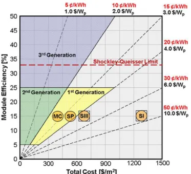
Recently, the energy and environment are two of the most important issues around the world. These included greenhouse effect and energy crisis persecute people for a few decades. Some scientists predicted that the fossil fuel, the main resources for world energy supply, would be depleted in the nearly future [1-1]. Also, increasing of environmental pollution related to the usage of fossil fuel lead us to search the best ways of using the local renewable resources of energy. The substitute energy such as solar, tides, wind, and geothermal heat are all renewable and pollution-free. Among them, solar energy is a promising candidate because of its enormous energy about 1000 W/m2 and eternity against the whole human life. The first modern photovoltaic cell was developed at Bell Laboratories in 1954 [1-2], and the conversion efficiency is about 6%. But it was just too low to be applied. So, there are many researchers involving in efficiency enhancement. But for the applications in practice, not only the efficiency enhancement but the cost of manufacturing and starting materials is also something to be considered. In general, solar cells can be classified into three types, or called three generations. The first generation is wafer-based silicon solar cell, but it would be eventually replaced by the second generation of lower cost thin film technology (amorphous silicon, small organic modules, dye-sensitized oxide nanoparticles, etc) [1-3]. However, the development of second generation solar cell still be constrained by the problems of the low electro-optical conversion efficiency. As we know from above, in its most mature form of photovoltaic, high efficiency and low cost is the trend as called third generation solar cell, observed from Fig. 1.1[1-4].
2
Fig. 1.1 : Classification of three generation solar cells and its cost per peak watt ($/Wp)
1.2 Nano-crystalline Si Quantum Dots for Third Generation Solar Cell
1.2.1 Concept of the Third Generation Solar Cell
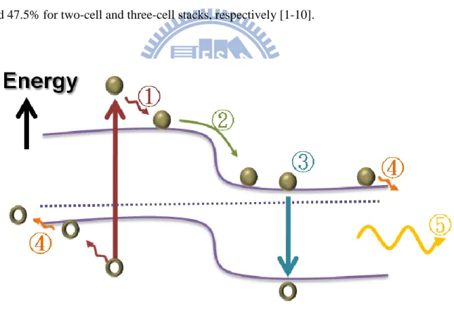
Today crystalline silicon wafer-based solar cells dominate the market. The record conversion efficiency for the first generation is about 25% [1-5], which nearly approaches the theoretical limitation (Shockley-Queisser limitation) value of 29%. Meanwhile, the starting material cost has to be reduced as well. Therefore, the new generation solar cells with higher efficiency and lower cost are the developmental trends. The third generation is the concept for the thin film second generation technologies of low cost and with increasing the efficiency of the photovoltaic devices [1-6]-[1-7]. One of the methods for efficiency enhancement is to reduce the energy loss paths as light absorbed by the material.As shown in Fig. 1.2, the two most important power losses are the energy higher than bandgap called high energy photon loss, and low energy photon loss of below bandgap photons [1-8]. Longer wavelength is not
3
absorbed by the material, and shorter wavelength generates an electron-hole pair but relaxation to conduction and valance band edge as heat. All of these limit the electro-optical conversion efficiency. Upon above reasons, there are some kinds of third generation solar cells tuning bandgap, called bandgap engineering, to reduce the two energy loss paths. For example, solar cells of CIGS achieve bandgap engineering by adjusting gallium content in the active layer [1-9]. And in our study, we adjust different size of nano-scale silicon quantum dots (QDs) to do so [1-8]. By stacking structure, with the highest bandgap cell on the top and the photons less than its bandgap pass through to lower bandgap underneath, each cell converts part of the solar spectrum at maximum efficiency. As a result, the efficiency can be totally enhanced. For instance, the over-all conversion efficiency can be reached for 42.5% and 47.5% for two-cell and three-cell stacks, respectively [1-10].
Fig. 1.2 : Loss mechanisms in a single bandgap solar cell: (1) high energy photon loss, (2) junction loss, (3) recombination loss, (4) contact voltage loss (5) low energy photon loss
4
1.2.2 Principles of Si Quantum Dot Thin Film Solar Cell
As the size of the structure is reduced to a few nanometers, the phenomenon of quantization occurred. The quantum confinement, achieved by restricting at least one dimension less than the Bohr radius of the bulk crystalline silicon (about 5nm), cause the discrete energy level. The strongest quantum confinement effect (QCE) is obtained if the silicon is constrained in three dimensions, as in quantum dots. By adjusting the size of Si QDs, the effective bandgap can be controlled. Base on these principles, the Si-QD thin film solar cells can realize bandgap engineering and reach high electro-optical conversion efficiency by stacking structure. One of the advantages for Si-QD thin film solar cell is that it can be fabricated by all silicon-based tandem solar cells, because of well-developed for silicon technology in IC industry. And silicon is also one of the most abundant elements on the earth. So far, many groups for the researches of Si-QD thin film solar cell are fabricated by using nanocrystal silicon QDs embedded in the Si-based material such as SiO2, Si3N4, and SiC
[1-11]. If these Si-QDs are spaced close enough, there is a significant overlap of the electron wavefunction. That means the carriers can transport between spaced Si QDs. However the experimental results are still substantially lower than the theoretical value. It can be attributed to the unfavorable material characteristics of these Si-based matrices, that is, they are not electrically conductive. The carrier transport through the dielectric matrix is by tunneling. It would complete limit the ability of carrier transportation. For such a terrible drawback mentioned above, we propose to use Zinc oxide (ZnO) as the substitutable matrix material for many potential applications and unique features over other conventional wide band gap semiconductors such as high transparency, nice crystallinity, and easiness to control the electrical properties [1-12]. Hence, ZnO is a suitable material to serve as the matrix for
5
nano-crystalline Si thin film solar cells.
1.3 Paper Review
1.3.1Characteristics of ZnO Thin Film and ZnO/Si Hetrojunction Solar
Cell
ZnO is a II-VI compound semiconductor with wurtzite structure [1-12]. The wurtzite structure has a hexagonal unit cell with two lattice parameters a and c in the ratio of c/a = 1.633 (in an ideal case). Recently, ZnO thin films have received much attention in a view of optoelectronic device applications. The characteristics included transparency, nice crystallinity, wide bandgap semiconductor material, and direct bandgap also shown in 0. Highly tunable electrical properties are appealing for the electric-related applications [1-12]. And most of all, it is not a rare element so that the cost for the material is not a big deal. It makes an economic superiority for its applications. Because of the native n-type properties of ZnO, there are some group studied the solar cell with n-type ZnO deposited on p-type Si wafer, made a hetrojunction solar cell [1.20].
Fig. 1.3 : (a)α 2 vs hv curves for the optical bandgap determination in as-grown ZnO and annealed ZnO samples, (b)XRD pattern of the as-grown ZnO thin film
6
1.3.2 Si Quantum Dot Solar Cell
Several techniques have been realized for fabricating the Si-QD thin film solar cells. The methods included different deposition machines such as molecular beam epitaxy [1-13], Si implantation [1-14], or phase separation of Si-rich-oxide by a sputtering [1-15] etc. Among them, the sputtering is a suitable manufacturing machine due to easiness controlling the size of Si-QD and its distribution. It is also a simple and cheap machine that has extensive been applied in the semiconductor industry. The nano-crystalline Si (nc-Si) QDs can be realized by the superlattice structure, deposited silicon rich oxide (or silicon rich nitride, silicon rich carbide) layer and silicon dioxide (or Si3N4, SiC) layer alternately. And after high temperature
post-annealing, the excess silicon precipitate to form nc-Si QDs from silicon-rich oxide (SRO) layer. By this way, the dots size can be clearly defined by controlling the thickness of each SRO layer. There are three different materials to serve as a matrix with Si-QDs embedded, that is SiO2, Si3N4, and SiC. And after a high temperature post annealing, Si QDs formed. It
can be observed as equation (1-1) [1-8].
(1-1)
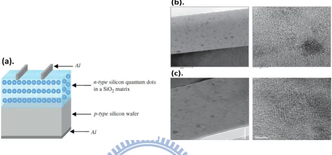
In Fig. 1.4, the Si-QD thin film solar cell for silicon dioxide as the matrix material was fabricated by sputtering [1-16]. The sample was fabricated by the phosphorous-doped Si-QDs supperlattice as an active layer on the p-type crystalline Si wafer as shown in Fig. 1.4 (a). By changing the thickness of the Si rich oxide (SRO) layer, the dots size can be precisely controlled. First of all, we observed the dot size of the Si-QDs by high-resolution transmission microscopy (HRTEM). Fig. 1.4 (b) shows the low-magnification and high resolution TEM image of bright-field mode for the annealed sample at 11000C with 5nm silicon dot size, and
7
(c) with 8nm dot size. As a result, observed from HRTEM, we can exactly control the size of Si-QD after high-temperature annealing, and just as our predicted, the thicker SRO layer is, the larger size of Si-QDs will be.
Fig. 1.4 : (a) Schematic diagram of n-type Si QDs on the p-type c-Si hetrojunction solar cell and TEM images of Si quantum dots in a SiO2 matrix with low-magnification and
high-resolution lattice images for (b) 5nm and (c) 8nm Si QDs.
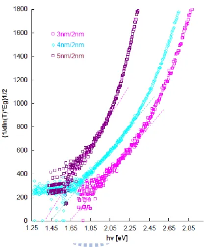
Second, the optical variation between different dots size can be seen as Fig. 1.5. The optical band gap ( Eopt ) was extracted from Tauc‟s function as α hν = 0, observed from
equation (2), where h is Planck‟s constant, ν is the frequency of the radiation, and BTauc is the edge width parameter [1-17].
α ν ν (1-2)
8
From (α hν )1/2
versus photon energy shown in Fig. 1.5, there is an evidence that the effective bandgap shift to higher photon energy with the dots size been smaller.
Fig. 1.5 : (α hν )1/2 versus photon energy with different size of Si-QDs
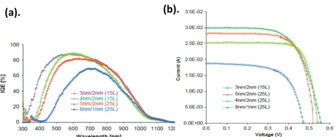
The phenomenon is consistent with QCE. And then we focused on the optical-electrical properties for photovoltaic, these are, the spectral response and its optical-electrical conversion efficiency. From Fig. 1.6 (a) and (b), these showed the spectral response and I-V characteristic with different thickness of SRO layers, respectively. Finally, we observed the highest efficiency of 10.58% from the structure of 3nm SRO layer apart from 2nm SiO2 layer
9
SiC [1-19].
Fig. 1.6 : (a) The spectral response with internal quantum efficiency (IQE), and (b) showed I-V characteristics of the cell for 3, 4, 5, and 8nm Si-QDs
Table 1-1 : 1-Sun illumination cell of four different n-type Si QDs/ p-type c-Si heteroface devices measured at 298K
10
1.4 Experimental Motivation
As shown above, the efficiency of Si-QD solar cell is mainly limited by the dielectric characteristics such as SiO2, Si3N4, and SiC. So far, the record efficiency of the Si-QDs solar
cell was about 10.6% published by the group of M.A. Green [1-16]. However, it‟s still not enough. That is due to the carrier transportation barrier coming from the dielectric characteristics of the matrix constrained the current conductivity [1-11]. As a result, we proposed ZnO as a new matrix material because it is a good electrically conductive. The un-doped ZnO thin film shows a high conductivity due to the electron density as high as 1021cm-3 [1-12]. It is naturally an n-type semiconductor. And ZnO is a good crystalline structure with preferential orientation along (0002) axis in the ZnO films. It also shows high transparency characteristics. Such a lot of advantage mentioned above, we propose to use ZnO to serve as the matrix material for nc-Si QD thin film solar cell.
In the studies, the substitution for ZnO as a new matrix material is an appealing idea to enhance the ability of carrier transportation. We proposed the structure as the ZnO thin layer and Si thin layer deposited alternately, by the RF magnetron sputtering. The Si atoms will self-assemble as clusters beyond the finite thickness of the Si layer. And after high-temperature post annealing, the Si-QDs formed. We analyzed the structural, optical and electrical properties of the ZnO thin film with silicon quantum dots embedded. The schematic diagram is shown in Fig 1.7.
11
12
Reference
[1-1] S. Shafiee, E. Topal, “When will fossil fuel reserves be diminished?,” Energy policy
37, pp. 181-189 (2009)
[1-2] D.M. Chapin, C.S. Fuller, G.L. Pearson, “A New Silicon p-n Junction Photocell for Converting Solar Radiation into Electrical Power,” J. Appl. Phys. 25, pp. 676 (1954) [1-3] M. Gratzel, “Photovoltaic and photoelectrochemical conversion of solar energy,”
Philos. Trans. R. Soc. London, Ser. A 365, pp. 993-1005 (2007)
[1-4] H. W. Hillhouse, M. C. Beard, “Solar cells from colloidal nanocrystals: Fundamentals, materials, devices, and economics,” Current Opinion in Colloid &
Interface Science 14, pp. 245-259 (2009)
[1-5] M. A. Green, K. Emery, Y. Hishikawa, and W. Warta, “Solar cell efficiency tables (version 37) ,” Prog. Photovolt: Res. Appl. 19, pp. 84-92 (2011)
[1-6] M. A. Green, “Third generation photovoltaics: Ultra-high conversion efficiency at low cost,” Res. Appl. 9, pp. 123-135 (2001)
[1-7] M. A. Green, “Recent developments and future prospects for third generation and other advanced cells,” 4th WCPEC (32nd IEEE-PVSC), Hawaii, pp. 7-12 (2006) [1-8] E. C. Cho, M. A. Green, G. Conibeer, D. Y. Song, Y. H. Cho, G. Scardera, S. J. Huang,
S. Park, X. J. Hao, Y. D. Huang, and L. V. Dao, “Silicon quantum dots in a dielectric matrix for all-Si tandem solar cells,” Adv. Optoelectron., pp. 69578/1–69578/11 (2007) [1-9] M.A. Contreras, K. Ramanathan, J. AbuShama, F. Hasoon, D. Young, B. Egass,
R.Noufi, “Diode characteristics in state-of-the-art ZnO/CdS/CuIn(1_x)GaxSe2 solar cells,” Progress in Photovoltaics 13, pp. 209-216 (2005)
[1-10] M.A. Green, “Third generation photovoltaics : advanced solar energy conversion,”
Springer, Berlin, Germany (2003)
[1-11] M.A. Green, E. C. Cho, Y .H. Cho, E. Pink, T. Trupke, K.L. Lin, T. Fangsuwannarak, T. Puzzer, G. Conibeer and R.Corkish, “All-silicon tandem cells based on „artificial‟ semiconductor synthesised using silicon quantum dots in a dielectric matrix” Proc.
20th European Photovoltaic Solar Energy Conf. (Barcelona, Spain), pp. 3 (2005)
[1-12] Ü. Özgür, Ya. I. Alivov, C. Liu, A. Teke, M. A. Reshchikov, S. Doğan, V. Avrutin, S.-J. Cho, and H. Morkoç, “A comprehensive review of ZnO materials and devices,” J.
Appl. Phys. 98, pp. 041301-0415403 (2005)
[1-13] Z. H. Lu, D. J. Lockwood, and J.-M. Baribeau, “Quantum confinement and light emission in SiO2/Si superlattices,” Nature 378, pp. 258–260 (1995)
[1-14] T. Shimizu-Iwayama, S. Nakao, and K. Saitoh, “Visible photoluminescence in Si+-implanted thermal oxide films on crystalline Si,” Applied Physics Letters 65, pp.
13
1814–1816 (1994)
[1-15] E.-C. Cho, S. Park, X. Hao, D. Song, G. Conibeer, S.-C.l Park and M.A. Green, “Silicon quantum dot/crystalline silicon solar cells,” Nanotechnology 19, pp. 245201 (2008)
[1-16] S. Park, E. Cho, D. Song, G. Conibeer and M.A. Green, “n-Type silicon quantum dots and p-type crystalline silicon heteroface solar cells”, Sol. Energy Mater. Sol. Cells 93, pp. 684 (2009)
[1-17] L. Ding, T.P. Chen, Y. Liu, C.Y. Ng and S. Fung, “Optical properties of silicon nanocrystals embedded in a SiO2 matrix,” Phys. Rev. B 72, pp. 125419 (2005)
[1-18] Y. Cho, E.-C. Cho, Y. Huang, T. Trupke, G. Conibeer, and M. A. Green, “Silicon quantum dots in SiNx matrix for third generation photovoltaics,” 20th European
Photovoltaic Solar Energy Conference, Barcelona, Spain, pp. 47 (2005)
[1-19] D. Song, E.–C. Cho, G. Conibeer, C. Flynn, Y. Huang and M.A. Green, “Structural, electrical and photovoltaic characterization of Si nanocrystals embedded SiC matrix and Si nanocrystals/c-Si heterojunction devices,” Sol. Energy. Mater. Sol. Cells 92, pp. 474 (2008)
14
Chapter 2 Sample Preparation and Analyses
2.1 Sample Preparation
In this chapter, we exhibit every process of our sample preparation and then introduce different analytical instruments and its principle. The schematic shown in Fig. 2.1 demonstrated the process from the beginning for the substrates clean to the end for the electrode deposition. After sample preparation, the different analysis methods had been done to show the characteristics of nc-Si quantum dots embedded ZnO thin films.
Fig. 2.1 : Sample fabrication process
2.1.1 Substrates Clean
There are two different substrates being used, p-type Si wafer and Quartzes. Upon different analyses, the substrates should be chosen differently. The quartzes were ultrasonically cleaned with acetone and alcohol for 10 minutes and the Si wafers were cleaned by H2SO4 and HF solutions to remove the particles and the native oxide layer.
Substrates clean Thin film deposition Post-annealing Metal deposition Electrical properties
Optical and structural properties
15
2.1.2 Thin Film Deposition
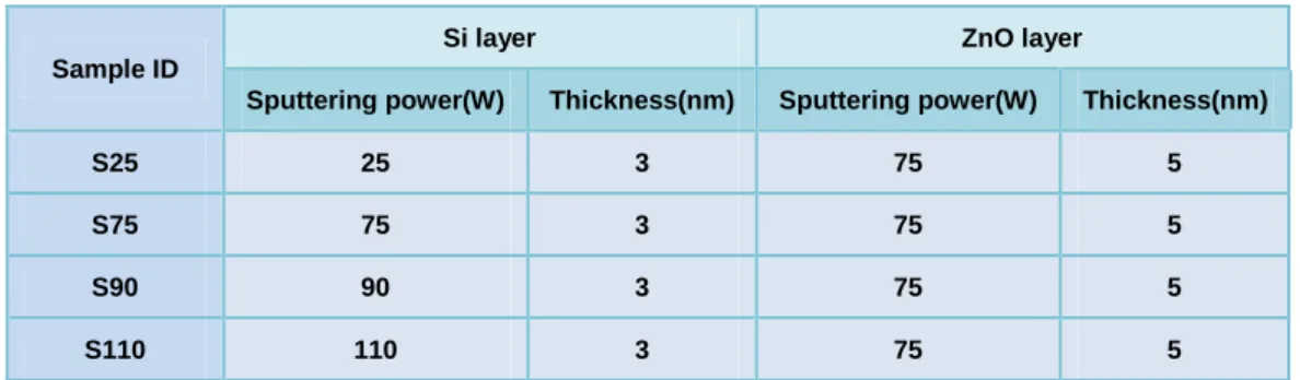
A variety of fabrication techniques can be observed to fabricate the Si-QDs nanostructures that are compatible with the standard IC industry: ion-implantation, molecular-beam exitaxy (MBE), radio-frequency (RF) magnetron sputtering, plasma enhanced chemical vapor deposition (PECVD), and pulsed laser ablation supersonic expansion. In our studies, we deposited the thin films by Rf magnetron sputtering. The sputtering is the physical vapor deposition technique that used Ar+ ion bombarded the target. And after the moment transformation, the vapor atoms from the target can be deposited onto the substrates. With magnetron techniques the ionization rate can be enhanced and also the chamber pressure can be reduced as 100 times below. The sputtering is a promising machine that can precisely control the thickness of the films and also has less containment in the films. In this study, ZnO/Si single-bilayer and 20-bilayers (ML) thin films were deposited on p-type Si(100) wafers and quartzes at a working pressure of 5 mTorr by radio-frequency (RF) magnetron sputtering method. The Si sputtering power (PSi) was varied from 25 to 110 W
while that of ZnO was fixed at 75 W, and the thickness of each ZnO and Si layers were fixed at 5 and 3 nm, respectively. The deposition parameter is listed as Table 2.1.
Table 2.1 : Sputtering parameters of ZnO/Si single bilayer and 20-bilayers (ML) thin films
Sample ID
Si layer ZnO layer
Sputtering power(W) Thickness(nm) Sputtering power(W) Thickness(nm)
S25 25 3 75 5
S75 75 3 75 5
S90 90 3 75 5
16
2.1.3 Post-Annealing Method
There are two post-annealing instruments we used, rapid thermal annealing (RTA) and Furnace. RTA refers to a manufacturing process which supplies a high temperature to the substrates on a timescale of several seconds or less. Compare to the RTA thermal process, the furnace is a slow heat process. The ramp rate is about tens of degree per minute. The significant difference between RTA and furnace make them on each purpose. But all of them can active the carriers or crystallize the material.
In our studies, the post annealing parameters can be classified into two parts, RTA process and furnace process. Each of them can further separate to some annealing conditions under different annealing temperature or different annealing time. Here shows the post annealing parameters as Table 2.2.
Table 2.2 : Post annealing parameters after deposition
Temperature Time ambient
RTA 10000C 20,50(seconds) N2 Furnace 7000C 5(mins) 8000C 9000C 10000C
17
2.1.4 Electrode Deposition
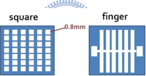
In the last step, metals are deposited for the electrical measurement. The ZnO thin film with Si-QDs embedded is regarded as an n-type film. As a result, we deposited Al as the top electrode. And the film is deposited onto the p-Si wafer, so the Ni is a better chosen for the back electrode. The different metal deposition is for the better contact when considering to the working function difference. The top electrodes are designed to the two patterns, the square and finger patterns. The finger is composed of a 5 mm x 0.1 mm rectangle, the bar is a 0.2 mm x 4 mm rectangle, the pad is a 1.2 mm x 0.7 mm rectangle and the spacing is 0.29 mm. The details of top electrode patterns are shown below in Fig. 2.2.
18
2.2 Sample Analyses
The analytical equipments included transmission electron microscopy (TEM), atomic force microscopy (AFM), Raman spectroscopy, X-ray diffraction (XRD), UV-visible, and 4156 are shown in this section. The ZnO thin films with nc-Si QDs embedded are investigated on the structural, optical, electrical properties by above analytical equipments.
2.2.1 Surface Morphology
In the thesis, the analyses for surface morphologies are investigated by a Digital Instrument D3100 atomic force microscopy (AFM) and a JEOL NPGS scanning electron microscopy (SEM). It can scan the difference of height precisely to the scale of nanometers by the AFM measurement [2-1]. There are three different modes when the probe scanning. One of them taps on the surface when the probe scans, called tapping mode. Our AFM images are obtained under tapping mode. The schematic is shown in the Fig. 2.3. By detecting the probe amplitude variation while scanning, we can identify the surface morphology precisely.
19
SEM is the equipment that images the sample surface by scanning it with a high energy beam of electrons raster scan pattern [2-2]. The image is observed by collecting the secondary electrons when the high energy electron beams bombard on the surface. Different numbers of the secondary electrons are generated at different surface morphologies which cause image contrast. The illustration is shown in Fig. 2.4. If a certain region on the sample more secondary electrons are produced, a brighter image will appear there.
20
2.2.2 Structural properties
In this section, the transmission electron microscopy (TEM) will be introduced. One of the critical proofs for the nc-Si QDs formation is the atomic arrangement structure images. TEM is a suitable instrument for the analyses with its fine structure. It is a microscopy technique whereby a beam of electrons is transmitted through an ultra thin specimen. These electrons interact with the atoms and showing the atoms arrangement images by the high resolution TEM [2-3]. The schematic of a typical TEM is shown in Fig. 2.5.
21
2.2.3 Crystalline property
In this section, X-ray diffraction (XRD) will be introduced. In our studies, the X-ray diffraction patterns were measured by a Bede-D1 X-ray diffractometer (XRD) with Cu Kα radiation (λ = 1.5418 Ǻ). It is a non-destructive instrument for the structural characteristic analyses. It included the information of lattice constants, geometry, orientation of single crystals, prefer orientation of poly crystals, and stresses, etc [2-4]. The X-ray, produced by a high energy electrons beam bombarded on the metal sheet, is incident on the specimen and producing the diffraction pattern by the plane of the atoms in the specimen. The schematic is shown in Fig. 2.6 [2-5].
22
Diffraction angle 2Θ is the angle with the diffracted X-rays comparing to the incident X-rays. When there is a constructive interference, which follows the Bragg‟s law, the diffraction peak is observed. The Bragg‟s law is shown in equation (2-1)
2
d
hklsin
hkl (2-1) Where the dhkl is the spacing between the atoms planes, λ is the incident X-ray wavelength.Θhkl is the angle between the atomic planes and the incident X-ray beam.
The XRD pattern can also estimate the size of crystals by Scherrer formula, shown in equation (2-2) B
BCOS
K
D
(2-2)Where D is diameter of the crystals, K is a numerical constant, B is the full width at half maximum, λ is the wave-length of the incident X-ray, and θB is the Bragg angle.
As a result, we observe the information of the crystalline orientation and the structural properties by the diffraction patterns as above-mentioned.
23
2.2.4 Optical Property
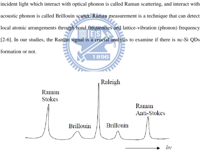
And then, we discuss the optical properties. The optical properties were measured by the Raman spectra which were examined using a 488 nm diode-pumped solid-state (DPSS) laser (HOROBA, Lab RAM HR). The illuminated spot size is about 1 um in diameter and the power of laser is about 50mW. Raman spectroscopy is based on the Raman effect, which is the inelastic scattering of photons by molecules. Here shows the Fig 2.7 for the three different signal produced by the incident light interaction with the specimen. The Releigh scatter is the elastic scattering. However the Raman scatter and Brillouin scattering are the inelastic. The incident light which interact with optical phonon is called Raman scattering, and interact with acoustic phonon is called Brillouin scatter. Raman measurement is a technique that can detect local atomic arrangements through bond frequencies and lattice-vibration (phonon) frequency [2-6]. In our studies, the Raman signal is a crucial analysis to examine if there is nc-Si QDs formation or not.
24
2.2.5 Electrical Property
The electrical property is measured by the 4156 equipment. The dark forward/reverse I-V curves can exhibit rectification ratio and obtain the properties of carrier transportation. And for the illumination analyses, the equipment is installed in the halogen light source with 1500 lux. As a result, we can investigate the photon response for our samples, and measurement the light current and its open voltage circuit, and short circuit current also.
25
Reference
[2-1] G. Binnig, C. F. Quate, C. Gerber, “Atomic Force Microscopy,” Phys. Rev. Lett. 56, pp.930 (1986)
[2-2] J. I. Goldstein, D. E. Newbury, P. Echlin, D. C. Joy, A. D. Romig, C. E. Lyman, C. Fiori, E. Lifshin, “Scanning Electron Microscopy and X-ray Microanalysis, a text for biologists,” materials scientists and geologists; Plenum Press: New York (1992) [2-3] D. B. Williams and C. B. Carter, “Transmission Electron Microscopy,” Materials
Science Plenum, New York (1996)
[2-4] G. Coa, “Nanostructures & Nanomaterials, Synthesis, Properties & Applications,”
Imperial College Press (2004)
[2-5] C. R. Brundle, C. A. Evans, and S. Wilson, “Encyclopedia of Materials Characterization, Surface, Interface,” Thin films, Butterworth-Heinedmann, USA, (1992)
[2-6] C. V. Raman, and K. S. Krishna , “ A new type of secondary radiation,” Nature 121, (1928)
26
Chapter 3 Experimental Results and Discussions
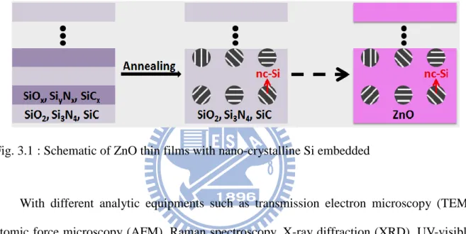
In our proposal, we replace the dielectric matrix material such as SiO2, Si3N4, and SiC to
ZnO for electrical properties enhancement in the silicon quantum dot solar cells. The schematic is shown in Fig. 3.1. This chapter investigates the characteristic of the nc-Si embedded ZnO thin films.
Fig. 3.1 : Schematic of ZnO thin films with nano-crystalline Si embedded
With different analytic equipments such as transmission electron microscopy (TEM), atomic force microscopy (AFM), Raman spectroscopy, X-ray diffraction (XRD), UV-visible, and 4156, we can know the properties of our device clearly. First of all, the characteristics of ZnO single layer must be investigated. These results are showed in section 3.1. Second, RTA annealing treatment has been used to form nc-Si. And after that, a series analyses will be demonstrated in section 3.2. Third, we substituted RTA to furnace as our post annealing equipment for some reasons. And the same analyses have been done in section 3.3. In the last section, we try to find out the solutions for film bending problem.
27
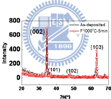
3.1 ZnO Thin Films
The crystalline quality of ZnO is one of our concern issues because it has strong influences on the optical and electrical characteristics [3-1]. Fig. 3.2 shows the XRD 2θ scan pattern for the ZnO film deposited on the quartz substrate. There are two lines under different thermal treatments, as-deposited process and annealed process by furnace at 10000C for 5min, respectively. These results illustrate that there is a good crystalline structure with preferred orientation along (0002) axis in the ZnO films, both on as-deposited and annealed samples. The crystalline properties of ZnO thin film can be enhanced under a high temperature post annealing.
Fig. 3.2 : XRD pattern of the as-deposited and annealed ZnO thin films, respectively
28
Then, we discuss its optical characteristics by Raman spectrum and UV-visible spectroscopy. The optical energy bandgap (Egopt) was estimated by assuming a direct
transition between valance and conduction bands from equation (3-1) [3-2], where A is a constant, hν is the energy of incident light, α is the absorption coefficient
α ν ν (3-1) As a result, we observed the optical bandgap of the ZnO thin film after annealing by furnace at 10000C for 5min is about 3.29 eV shown in Fig. 3.3 (a). And this result is matched with the literatures [3-2]. As a result, ZnO is a wide bandgap material which is suitable to serve as matrix for nc-Si QD solar cell. At Raman spectroscopy, there is a peak at about 435 cm-1 shown in Fig. 3.3 (b). It is contributed from oxygen-related mode (E2-high mode) of ZnO [1-13].
Fig. 3.3 : (a) Plots of (α hv)2 versus hv and (b) Raman spectrum of the ZnO film after annealing
29
At the electrical properties, the sheet resistance (Ω-cm) is calculated by the 4-point probe measurement. The calculated values are reported in Table 3.1. We observe that the sheet resistance will be reduced with raising the post annealing temperature. It may be attributed to the high temperature annealing which can improve crystalline quality of the ZnO thin film and increase the defect density such as oxygen vacancies Vo and zinc interstitial atoms Zni.
Therefore, it reveals that the conduction characteristics of the ZnO thin film can be enhanced by post annealing process.
Table 3.1 : Four-point probe measurement of ZnO film under different annealing conditions
As-deposited F300-5min F600-5min F1000-5min ZnO ERROR RROR 1.6E 1.3E-1
30
3.2 ZnO/Si Multilayer Thin Films with Rapid Thermal Annealing
Process
In this section, the ZnO/Si multilayer thin films were annealed by rapid thermal annealing (RTA) at 10000C for 20 and 50 seconds, respectively, in a N2 environment. The
series analyses are demonstrated below.
3.2.1 Structural Properties
First of all, we investigate the atomic arrangement structure images by high resolution transmission electron microscopy (HRTEM). The HRTEM images of sample S110 are shown in Fig. 3.4. In Fig. 3.4 (a), it exhibits obviously layer by layer structures in the as-deposited sample. For the high-magnification image shown in Fig. 3.4 (b), the ZnO thin layer and amorphous silicon nano-clusters can be seen clearly. The multilayer structure of sample S110 is still available after annealing at 10000C for 50 seconds shown in Fig. 3.4 (c). From Fig. 3.4 (d), the high density of nano-crystalline clusters with size range from 2 to 5 nm is in evidence, observed in high magnification cross section image of HRTEM. It is a good result for our devices.
31
Fig. 3.4 : Overall and zoom-in cross-sectional HRTEM images of ZnO/Si multilayer thin films. (a) and (b) are as-deposited, and (c) and (d) are after annealing for sample S110
3.2.2 Crystalline Properties of Nano-crystalline Si Quantum Dot
From above results, we observe a high crystalline density inside the ML thin films. In this section, we want to investigate the nc-Si formation in our structures. Raman is a simple, fast, and easy instrument to detect the presence of nc-Si QDs. The Raman spectra of the ZnO/Si multilayer thin films on quartzes under different Si sputtering power (Psi) are
exhibited in Figs. 3.5. In Figs. 3.5 (a) and (b), there are two different annealing conditions: RTA at 10000C for 20 (R1000-20s) and 50 seconds (R1000C-50s), respectively. We observed that there are two main peaks at ~435 cm-1 and ~518 cm-1. From literatures, we know that the peak at ~435 cm-1 is contributed from oxygen-related mode of ZnO [1.13], and the one at ~518 cm-1 comes from the formation of nc-Si [3.3]. It is clear that the peak at ~518 cm-1 is not
32
observed in sample S25 and significantly increases from samples S75 and S90 to S110, both in different annealing conditions. Therefore, a high enough PSi is necessary for the formation
of nc-Si embedded in the ZnO matrix.
Fig. 3.5 : Raman spectra of ZnO/Si multilayer thin films under different Si sputtering powers annealed by RTA (a) at 10000C for 20 seconds, (b) at 10000C for 50 seconds
Then, after knowing that Psi is a critical condition for nc-Si formation, we further
analyze the variation of nc-Si signal under different annealing conditions. The curve-fitting results for the peak at ~518 cm-1 contributed from nc-Si are listed in Table 3.2. We observed that the nc-Si signal can be enhanced with respect to a narrower FWHM, larger peak intensity area, and higher crystallinity by a longer post annealing time. All of these results shown above represent a better crystallization of nc-Si [3-3]. The crystallinity is estimated by equation (3-1), where Inc is the signal of nc-Si, and Ii and Ia are represented signal of intermediate Si and
amorphous Si, respectively.
(3-1) a i nc i nc
I
I
I
I
I
ity
crystallin
33
For nc-Si formation, a better annealing condition is RTA at 10000
C for 50 seconds. Therefore, the following analyses are according to this annealing condition.
Table 3.2 : Parameters of multilayer thin films under different annealed conditions
3.2.3 Crystalline Properties of ZnO Matrix
In our proposal, ZnO is regarded as a matrix, which provides good conductive properties. The better crystal quality of the ZnO thin film is, the better conductive property it will be. As a result, how to obtain a good quality of ZnO thin films is something what we want to figure out. The crystalline properties of the ZnO matrix for the multilayer thin films deposited on different substrates after annealing at 10000C for 50 seconds are analyzed from XRD patterns, as shown in Fig. 3.6. In Fig. 3.6 (a) the multilayer thin films deposited on quartz exhibit narrower FWHM with increasing PSi. In Fig. 3.6 (b), although there is a substrate effect [3-4]
for the multilayer thin films deposited on Si wafer, the same tendency as for quartz is observed. This means for better crystallization of the ZnO matrix, a high enough PSi is
34
Fig. 3.6 : XRD patterns of the ZnO/Si multilayer thin films deposited on (a) quartz, (b) Si (100) wafer under different Si sputtering powers after annealing
3.2.4 Influence of Surface Morphology
Fig. 3.7 shows the AFM images for the single ZnO layer with a 5 nm thickness and the single bi-layer thin films under different PSi on Si wafer after deposition. Significant
variations on the surface morphologies are observed. The surface roughness of samples S75, S90, and S110 are larger than that of the single ZnO layer and increase with increasing PSi.
More obvious formation of nano-clusters can be found for larger PSi. However, the AFM
image of sample S25 shows a smaller surface roughness than that of the single ZnO layer, and the deposited Si layer can be seen as a thin layer-like. Since a Si nano thin film with a 3 nm thickness needs a higher crystallization temperature of 1100°C than that for Si nano-clusters [3-5], the nc-Si is harder to efficiently form in sample S25 during the RTA process than samples S75, S90, and S110 and compounds are possibly produced [3-6]. From these results, an obvious aggregation of the sputtered Si atoms during deposition is helpful for the formation of nc-Si and the better crystallization of the ZnO matrix in the nc-Si embedded ZnO
35
thin films during the RTA process.
Fig. 3.7 : AFM images of (a) the single ZnO layer with a 5 nm thickness and the single ZnO/Si bilayer thin films under Psi of (b) 25 W, (c) 75 W, (d) 90 W, and (e) 110 W on Si wafer
after deposition.
In order to obtain more evidence for these results we observed from Fig. 3.7. A series experiments included deposition the single ZnO layer, ZnO/Si single bi-layer, single tri-layer, and single quadric-layer as Psi under 25 W and 75 W, respectively, are demonstrated by AFM
images as shown in Fig. 3.8 (a) to Fig. 3.8 (g). We observed that when Psi is 25W, after
depositing the Si thin layer, the surface become smoother compared to that of single ZnO layer. However after depositing Si layer under Si sputtering power of 75W, the surface gets rougher. And then the rougher surface become smoother as ZnO thin film with a 5nm thickness was re-deposited. The tendency is consistent in bi-layer, and quadri-layer under Si sputtering power of 75W shown in Fig. 3.8 (e) and Fig. 3.8 (g). It can‟t be seen as Psi under
25W. As a result, it shows that the deposited Si layer which can be seen as a thin layer-like under Psi equal to 25W. And when the Psi is higher than 75W, the sputtered Si atoms have
more kinetic energy to aggregate together as Si nano-clusters. The surface become rougher after depositing.
36
Fig. 3.8 : AFM images of (a) ZnO single layer with a 5nm thickness and (b) after deposited Si layer under Psi of 25 W for 3nm thickness, (c): re-deposited ZnO thin layer on (b) with a 5nm
thickness, and (d): re-deposited Si layer under Psi of 25 W for 3nm thickness on (c), the
deposition steps of (e), (f), and (g) are similar to (b), (c), and (d) just adjusting Psi from 25 W
to 75 W
3.2.5 Electrical Properties
For the solar cell applications, the electrical properties are one of the most important characteristics we concerned. In Fig. 3.9, ZnO/Si multilayer films under different Psi of (a) 25
W, (b) 75 W, (c) 90 W, and (d) 110 W, are studied on I-V characteristics. The sample S75, S90, and S110 show significant rectification ratio and good photo-response characteristics, but S25 doesn‟t. It concludes that Psi higher than 75 W is necessary of ZnO/Si multilayer films for
good electrical characteristic after annealing. The results are consistent with what we observed from Raman spectra, and XRD patterns. It reveals that the good electrical characteristics are contributed from the formation of nc-Si and the high crystal quality of ZnO matrix. As a result, a high enough PSi is necessary for the high-quality nc-Si embedded ZnO
37
thin films.
Fig. 3.9 : Dark forward/reverse I-V curves of ZnO/Si multilayer thin films under different Psi
of (a) 25W, (b) 75W, (c) 90W, and (d) 110W after annealing. The inset figures show the photo-response characteristics of the ZnO/Si multilayer thin films.
38
Table 3.3 is the quantitative analysis for the electrical characteristic obtained from Fig. 3.9 The rectification ratio at ±3V are enhanced on the order of 104, and the ratio after illumination at 0V are reached the order of 102 in sample S90. It concluded that the better rectification and good photo-response are observed with a higher Psi.
Table 3.3 : Electrical properties of ZnO/Si multilayer thin films under different Psi
It shows the formation of nc-Si and the better crystallization of the ZnO matrix under higher Psi than 75W, and result in good photo-response and significant rectification in the nc-Si embedded ZnO thin films during the RTA process. However, there are some problems existing during RTA thermal treatment. There is no open circuit voltage (Voc) observed in one of them.
39
3.2.6 Problems during Rapid Thermal Annealing Process
The multilayer of sample S110 is shown in Fig. 3.10. As mentioned above, we confront the problems which is no Voc observed in one of them. In Fig. 3.10 (a), the TEM image with low magnification exhibit some problems caused by RTA thermal process. First of all, at the top of the deposited film, there is a thick layer with about a 100 nm thickness. The extra thick layer is also observed after annealing, it shows in Fig. 3.10 (b). The thick layer is composed of Zinc and Oxygen, and each element is almost accounted for 50%, with the composition analysis by energy-dispersive X-ray (EDX). A slight Si content can also be measured in the thick layer. Second, there is approximate 5nm thickness of silicon oxide layer between the Si wafer and the deposited thin films. Third, there is a large bending degree at the interface after annealing. All of these may lead to no Voc observed in thess case.
Fig. 3.10 : The ZnO/Si multilayer films after annealing shown in (a) TEM image, (b) SEM image, (c) and (d) the interface between deposited films and Si substrate with high
40
3.3 ZnO/Si Multilayer Thin Films with Furnace Annealing Process
Fig. 3.11 : Schematic of the furnace
Because of the problems caused by RTA thermal treatment, we look for a new post annealing equipment to substitute. We use furnace as our new thermal treatment equipment, and its schematic is shown in Fig. 3.11. It is one side open, and at the other side purging the N2 gas to maintain the positive pressure inside the quartz tube. The sample was pushed into
the center of the tube with a rate at about 60 cm/min. After a period of thermal treatment at the center, the sample was pulled out at the same rate. In order to be similar to RTA thermal treatment, not only pushing and pulling out the sample at a high rate (60 cm/min), but also holding a short time (5min) during high temperature annealing. A series analyses are exhibited at following sections, and we investigate the characteristics for the ZnO thin films with nc-Si embedded after annealing by furnace.
41
3.3.1 Different Annealing Temperature
Fig. 3.12 : Raman spectrum of sample S110 with different annealing temperature from 7000C to 10000C for 5min
The annealing temperature at 10000
C is a good condition for nc-Si formation upon thermal process by RTA. But as the new post annealing equipment being used, the best annealing condition may be changed. As a result, the sample S110 annealed by furnace with different annealing temperatures for 5min are investigated in Fig. 3.12. We observed that the peak at about 480 cm-1 decreasing and the one at ~518 get more obvious with increased temperature from 7000C (F700) to 10000C (F1000). From literatures, the peak at 480 cm-1 is contributed to amorphous Si, and the one at ~518 cm-1 comes from the formation of nc-Si [3.3]. It obtained that with increasing the annealing temperature from 7000C to 10000C, the amorphous Si will translate to nc-Si.
42
In Table 3.4, it shows a clearly comparison for nc-Si signal between different post annealing temperature both on its FWHM, intensity area, and crystallinity. We observed that the nc-Si signal can be enhanced by a higher temperature annealing with respect to a narrower peak FWHM, larger peak intensity area, and higher crystallinity. As a result, a high temperature post annealing at 10000C is necessary for nc-Si formation by furnace thermal treatment.
Table 3.4 : Parameters of sample S110 under different annealing conditions
After Raman analyses, the electrical properties are investigated as shown in Fig. 3.13. We observed the good electrical properties of sample S110 for annealing temperature at 10000C by furnace. The quantitative analyses are listed in Table 3.5. We observed that with increasing the post annealing temperature, the Voc can be larger simultaneously. It may be attributed to the nc-Si formation obtained from Raman spectrum. As sample S110 annealed at 8000C for 5 min (F800-5min), there is a bad rectification ratio and no Voc observed. It might be attributed to the intermediate region from amorphous Si to nc-Si with annealing at 8000C for 5 min.
43
Fig. 3.13 : Dark forward/reverse I-V curves of sample S110 with different annealing temperature at (a) 7000C, (b) 8000C, (c) 9000C, and (d) 10000C for 5 min, respectively. The inset figures show the photo-response characteristics of sample S110.
Table 3.5 : Electrical properties comparison of sample S110 between different post annealing temperatures
44
3.3.2 Structural Properties
Fig. 3.14 : Cross-sectional TEM images with (a) low-magnification, (b) high-magnification of ZnO/Si multilayer thin films annealing by furnace at 10000C for 5min
The multilayer structure in sample S110 after annealing at 10000C for 5min by furnace is observed in Fig. 3.14 (a). And a high-magnification TEM image exhibit nc-Si formation, as shown in Fig. 3.14 (b). The dot size is about 3 or 4 nm shown in TEM images.
3.3.3 Crystalline Properties of Nano-crystalline Si Quantum Dot
The Raman spectra of the multilayer thin films on quartzes under different Si sputtering powers (Psi) annealed by furnace at 10000C for 5min are exhibited in Fig. 3.15. The similar
result obtained from RTA thermal treatment is also from furnace. There is no nc-Si signal observed in sample S25. And the signal of nc-Si significant increasedfrom sample S75 to S110. Therefore, a high enough PSi is necessary for the formation of nc-Si embedded in the
45
Fig. 3.15 : Raman spectra of multilayer thin films under different Si sputtering powers after annealing
We further analyze the signal of nc-Si obtained in Fig. 3.15. In Table 3.6, we observe the narrower peak FWHM, and larger peak intensity area with increasing Psi. It represents a better
crystallization of nc-Si.
46
3.3.4 Crystalline Properties of ZnO Matrix
The crystalline properties of the ZnO matrix for the multilayer thin films deposited under different Psi after annealing at 10000C for 5min by furnace are analyzed from XRD patterns,
as shown in Fig. 3.16. Both in Fig. 3.16 (a) and (b), the crystalline signal of ZnO (002) with 2 θ equal to 34.4 are observed. This means there is also a good crystallization of the ZnO matrix with furnace annealing process.
Fig. 3.16 : XRD patterns of sample (a) S75, and (b) S110