A Unified Approach to Profiling the Lateral
Distributions of Both Oxide Charge
and Interface States in n-MOSFET’s
Under Various Bias Stress Conditions
Shui-Ming Cheng, Cherng-Ming Yih, Jun-Chyi Yeh, Song-Nian Kuo, and Steve S. Chung,
Senior Member, IEEEAbstract— A new and accurate technique that allows the si-multaneous determination of the spatial distributions of both interface states(Nit) and oxide charge (Qox) will be presented.
The gated-diode current measurement in combination with the gate-induced drain leakage (GIDL) current were performed to monitor the generation of bothNit andQoxinn-MOSFET’s. A special detrapping technique and simple calculations have been developed, from which the spatial distributions of bothNit and
Qoxunder various bias stress conditions, such as the hot-electron stress(IG;max); IB;max; and hot-hole stresses, can be determined.
The calculation of gated-diode current by incorporating the extracted profiles of Nit and Qox has been justified from nu-merical simulation. Results show very good agreement with the experimental results. The extracted interface damages for hot-electron and hot-hole stresses have very important applications for the study of hot-carrier reliability issues, in particular, on the design of flash EPROM, E2PROM cells since the above stress conditions, such as theIG;max and hot-hole stress, are the major operating conditions for device programming and erasing, respectively.
I. INTRODUCTION
T
HE HOT CARRIER effect will induce the so-called gate oxide damages, which include the oxide-trapped charge and interface state at the Si- interface. In the past, much effort has been spent to characterize the localized distribution of interface states near the drain junction [1]–[3]; very few studies have been reported on the spatial distribution of the localized oxide chargePrevious studies [4]–[6] showed that simultaneous determi-nation of the interface states and oxide charge in MOS devices are rather difficult and not easy to implement. Thus far, only a few papers have reported achievement of this goal. The method by Chen et al. [4] used the conventional drain-substrate junction bias method, which will impose unintentional hot-carrier damage during measurement. The numerical method in [5] needs extensive numerical calculation. Both methods
can be used to determine both and under a hot
Manuscript received December 6, 1996, revised March 19, 1997. The review of this paper was arraged by Editor M. Fukuma. This work was supported by a grant from the National Science Council, Taiwan, R.O.C., under contract NSC84-2215-E009-053.
The authors are with the Department of Electronic Engineering and Institute of Electronics, National Chiao Tung University, Hsinchu 300, Taiwan, R.O.C.
Publisher Item Identifier S 0018-9383(97)07791-5.
electron or a hot-hole stress condition but not for both. In a recent paper by Tsuchiaki et al. in [6], only a special case for determining is dealt with. On the other hand, there are basically three different stressed conditions for hot electron or hot-hole stress, i.e, the maximum substrate current (we call this condition), the maximum gate current (we call this condition), and hot-hole stress conditions. The above three cases can only be restricted to the special stress conditions such as either hot electron or hot-hole stress. As a consequence, different approaches should be taken to deal with different stress conditions. It is the purpose of this study to find a generalized method that can be used to determine both and for devices stressed under various hot carrier stress biases.
In this work, we will develop a method for profiling both hot-electron-induced and hot-hole-induced interface damages. It is based on an improved gated-diode measurement technique with gate-induced drain leakage (GIDL) current as a monitor and a new characterization algorithm for determining and In Section II, the experimental devices and stress condition throughout this study will be described. In Section III, the principle of a new method using gated-diode measurement in combination with an algorithm to simultaneously determine and will be demonstrated. The results of spatial distribution of and at various hot carrier stress conditions will be presented and verified in Section IV. Finally, the conclusion of this study is given in Section V.
II. EXPERIMENTAL
The experimental devices used in this work were con-ventional n-MOS devices. The tested samples have 0.5- m mask channel length and 20- m channel width. The gate oxide thickness is 7 nm. The implant is 25 keV, 3 10 cm BF , and the source/drain region was performed by using arsenic implant with an energy of 80 keV and a dose of 5 10 cm The channel profile and source/drain profile have been calibrated against SIMS data. For the hot carrier stress experiment, three different bias stress conditions have been performed. The first one is the hot electron stress
at V and V, where maximum gate current
(a)
(b)
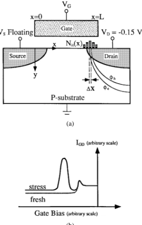
Fig. 1. (a) Schematic diagram of gated-diode current measurement setup, the contours of eand hat a drain voltageVD= 00:15 V for a forward-biased
drain-to-substrate junction are presented. Gate voltagesVGare varied from inversion to strong accumulation. (b) Qualitative expression of the measured gated-diode current(IGD) for device before and after the stress.
occurs. The second one is called hot-hole stress or
off-state stress at V and V, where the device
operates in the off state. The third one is called the
stress condition at V and V. Gated-diode
current and GIDL current measurements have been carried out using the HP 4145B parameter analyzer.
III. PRINCIPLE OF THE NEWMETHOD
The new approach adopts the gated-diode measurement technique in [7] and [8] for characterization and with addition of characterization. The gated-diode current measurement only requires simple dc current measurement and yields better spatial resolution such that this method is more convenient than charge pumping current method. A voltage is applied to the drain to forward-bias the drain-substrate junction, and the current is measured as a function of gate voltage [Fig. 1(a)]. In this work, we use a drain forward-bias of V, and the source terminal is left floating to avoid any potential drop along the channel. A typical I–V characteristic measured by gated-diode current measurement is illustrated in Fig. 1 (b), where both currents for a fresh device, and a stressed device can be seen. The difference between these two curves shows the additional recombination caused by the interface state.
According to Shockley–Read–Hall theory [9] and by
as-suming that , the surface component of
current is mainly determined by the recombination in the region where the electron and hole concentrations are nearly equal, that is, the surface potential is close to the midgap.
Fig. 1(a) contribute to the recombination current. Further,
with decreasing , moves toward the drain region.
The difference between the measured current of
devices before and after stress can be used to determine the spatial distribution of The excess recombination current
after the stress can be expressed as [7]
(1) where
device channel width; unit charge;
thermal velocity;
defect capture cross section;
current path where recombination current oc-curred;
intrinsic carrier concentration.
According to (1), we see that is a function of gate bias If there are oxide trapped charges in the region, they will cause the variation of Note that the interface states are simultaneously filled with electrons and holes between and such that the recombination current occurs only in this region. In the meantime, the interface states between and are neutral such that these traps do not cause the variation of , whereas oxide trapped charges (either positive or negative) will induce a shift of
In other words, the value of on the right-hand side of (1)
will be replaced by if there is present at
location of In this case, for a stressed device including both and , the increment of measured gated-diode current (1) should be modified as
(2)
Here, the measured gated-diode current is contributed
by both and
Based on (2), we will provide a new technique to determine spatial distributions of both and based on the basic gated-diode technique, which can only be used to determine distribution. The neutralization (or detrapping) technique and simple numerical calculation are used to determine distribution. To separate both and , the experimen-tal and numerical procedures are illustrated in Fig. 2 and described as follows.
1) Measure the gated-diode and gate-induced drain leakage currents on a fresh -MOS device with
Fig. 2. Flowchart of a new method to characterize the spatial distributions ofNit(x) and Qox(x):
source floating as shown in Fig. 1. The versus relationship near the drain junction is established by 2-D numerical simulation.
2) Measure the - and - characteristics for
devices after the hot-carrier stress.
3) Use a neutralization (or detrapping) step to neutralize (or detrap) the hot-carrier induced , and ensure that this step does not cause any stress or change (which can be verified by inspecting the magnitude of -current).
4) Using the recover current obtained by step 3), we can directly calculate the hot-carrier-induced by using (1) and versus the relationship. (The complete recovery of the oxide charge is verified by
the - current).
5) The hot-carrier-induced is obtained from the - curve before and after the neutralization step. In the flowchart of Fig. 2, the fresh, stressed, and neu-tralized (or detrapping) - currents can be obtained by the above experimental procedures (1)–(3). Values of and represent the chosen convergence criterion for iteration and the increment of oxide charge, respectively. In this new method, the distribution can be first extracted from the difference between fresh and neutralized
(or detrapping) currents by using (1). Then, the
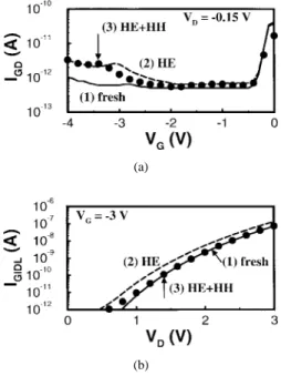
(a)
(b)
Fig. 3. (a) MeasuredIGDcharacteristics of the test device after IG;max stress atVD= 5 V and VG= 5:5 V. (b) Measured GIDL currents. Curves
(1) fresh (solid line); (2) hot electron stress (dashed line); (3) after hot hole detrapping (solid circles).
distribution will be determined by comparing the
stressed current with the simulated one, which
includes the and the superimposed profiles. In this profiling procedure, there are two iteration loops. The inner loop in the flowchart is to determine the value of oxide charge at a fixed gate voltage. The external loop varies the gate voltage such that we can determine the spatial distribution of oxide charges along the channel direction. is the total number of measured - characteristics. According to this methodology, the profiles of and for devices stressed at various bias conditions, such as off-state, maximum
substrate current and the maximum gate current
, can all be extracted. Details will be discussed in the next section.
IV. RESULTS AND DISCUSSION
A. Damage Generation During Hot Electron Stress
Fig. 3 shows the measured - and -
charac-teristics. Solid lines are the measured current for fresh devices. Dashed lines are the measured currents after hot electron stress
at V and V. currents will be used
for determining and , whereas is used for
monitoring the generation of interface state or oxide trapped charge. Under the above stress bias, it will generate not only
but negative as well. The peak value of
-curve is shifted to a more positive gate voltage region when the negative exists as shown by dash curve in Fig. 3. To extract the distribution of , we must neutralize this , and it was accomplished by hot-hole injection by the
band-to-band tunneling (@ V, V, for
10 s), as shown by solid circles in Fig. 3. The step for hot-hole injection does not cause any change in fresh
-Fig. 4. Extracted spatial distributions of Nit(x); Qox(x) and simulated
maximum lateral field for devices with hot electron stress atIG;max:
and - curves (which are not shown here), and the
peak value of - curve (solid circles) is shifted to more negative gate voltages, that is, the previous negative charges can be compensated by hot-hole injection. In addition, we may observe from the bottom figure in Fig. 3 that after the hot-hole neutralization step, the GIDL current (solid circles) has been reached to the original current level at large bias (e.g., V). This means that the oxide trapped charge has been filled with holes. The gated-diode current after this neutralization step is given in the top figure of Fig. 3, in which the solid circles give the current with only.
From the HE HH curve (curve 3) and the fresh -current (curve 1), can be extracted using the above method described in Section III. Once the has been extracted, we can easily use curve 3 (solid circles) and curve 2 (dashed lines) in the top figure of Fig. 3 to calculate the negative The extracted spatial distribution of and are given in Fig. 4, in which the lateral electric field is also shown for comparison. The location of maximum and is several hundred Angstroms away from the location of
maximum lateral field (@ V, V). Note
that the simulated maximum electric field is plotted along the surface direction. We also observed that and is localized in the gate-drain overlap region. Therefore, this result does not change the subthreshold current and is consistent with the experimental results (which are not shown here). To verify the accuracy of this method, the extracted and are put into the simulator to calculate the gated-diode current from (2); we found that the calculated result is in agreement with the experimental result, as shown in Fig. 5(a). The
versus relationship due to the and is also
shown in Fig. 5(b), in which the solid curve represents the simulated versus curve for the fresh device, and the long dash curve represents the versus curve with and The difference of these two curves at each position
is due to the existence of negative
B. Damage Generation After Hot-Hole Stress (Off-State Stress) To verify the efficacy of the new method, we also implement this method for the off-state stress condition at V and
(a)
(b)
Fig. 5. (a) Fresh and stressedVGversusx curves in which the difference for two curves results from the negativeQox(x) due to the hot electron stress.
(b) Comparison between the experimental and calculated gate-diode currents.
V for 5000 s. The - and - curves
for fresh, after hot-hole injection, and detrapping are shown in Fig. 6 with forward drain-substrate bias of V.
Here, we use the detrapping step (@ V, V for
500 s) to detrap the positive The peak value of -curve is shifted to more negative gate voltages after the hot-hole injection and is shifted to more positive gate voltages after the detrapping. This detrapping step will not cause any
stress in fresh - and - curves by repeating
the measurement. The extracted spatial distributions of and are given in Fig. 7. The peak value of extracted positive charges is beyond 1 10 cm and larger than the peak value of extracted interface states. The verification of the calculated gated-diode current with experimental data is shown in Fig. 8. The calculated gated-diode current is matches well with the experimental results. The bottom figure also shows the calculated - relationship in which the difference of two curves at any position is due to the existence of positive
C. Damage Generation at Maximum Substrate Current
The distribution of under the maximum substrate current stress condition is well understood [5], but the comparison of peak position and quantities for between the and are as yet unclear. To tell the difference,
- and - curves for fresh and stressed
condi-tions under are measured in Fig. 9(a) with a forward
drain-substrate bias of V and, in Fig. 9(b),
with gate bias of V, respectively. From the current of Fig. 9(b) and the subthreshold current (which is not shown here), we know that the generation is dominant, and the generation is neglected at stress since it can be observed from Fig. 9(b) that the currents for
(a)
(b)
Fig. 6. (a) MeasuredIGDcharacteristics of the test device after hot-hole stress atVD= 5 V and VG= 04 V. (b) Measured GIDL currents. Curves
(1) fresh (solid line); (2) hot electron stress (dashed line), (3) after hot-hole detrapping (solid circles).
Fig. 7. Extracted spatial distributions of Nit(x); Qox(x) and simulated
maximum lateral field for devices with hot-hole stress in Fig. 6.
fresh (curve 1) and stressed (curve 2) are the same at larger bias. The extracted distribution of and simulated lateral electric field at stress are given in Fig. 10. The peak value of is about 20 nm away from the peak of the electric field. We also found that values of at stress are larger than values of stress due to a larger
lateral field of than values of Furthermore, the
lateral fields for and are all located in the gate-drain overlap region, but the position of is far from the drain junction than those of , i.e., the lateral field of the stress case is moving toward the gate edge. This result
causes the peak position of the stress condition
located in front of the case.
Based on the above results, the advantages of the present method are as follows.
1) and can be simultaneously determined by using the neutralization (detrapping) technique and simple
(a)
(b)
Fig. 8. (a) Fresh and stressedVGversusx curves in which the difference for two curves results from the positiveQox(x) due to the hot-hole stress.
(b) Comparison between the experimental and calculated gate-diode currents.
numerical calculation. It is very easy to implement based on simple dc measurement, and no complicate numerical iteration is needed to extract and
2) Lateral distributions of both and can be obtained
under any stress conditions, such as and
hot-hole stresses.
3) The gated-diode technique is much better than the charge pumping method in terms of the feasibility for probing oxide damages deeply into the gate-drain overlap region. In other words, the gated-diode technique can detect a wider range of damage distribution (see [7], Fig. 7).
V. CONCLUSION
In summary, we have successfully demonstrated a new method to separate the from the and to determine their spatial distributions for devices under various stress conditions such as , off-state stress, and maximum substrate current biases. Several salient features are the following.
1) We present for the first time a generalized method for device oxide damage characterization no matter whether there are hot-electron or hot-hole stress conditions. 2) The results have very important applications for studying
flash EPROM reliabilities since is the operating bias for hot carrier programming, and the generated during the erase operation corresponds to the off-state stress bias that we used.
3) The gated-diode measurement technique is well suited for probing device oxide damage in the gate-drain over-lap region with good accuracy.
Finally, the developed technique is very simple to implement in profiling the hot-electron-induced and hot-hole-induced damage for submicron or deep-submicron MOSFET’s, and in particular, it is useful for flash EPROM, E2PROM device
(a)
(b)
Fig. 9. (a) Measured IGD characteristics of the test device after IB;max stress atVD= 5 V and VG= 2 V. (b) Measured GIDL currents. Curves (1)
fresh (solid line); (2) hot electron stress (dashed line).
Fig. 10. Extracted spatial distributions ofNit(x) and simulated maximum lateral field for devices withIB;max stress in Fig. 9.
REFERENCES
[1] M. G. Ancona, N. S. Saks, and D. McCarthy, “Lateral distribution of hot-carrier-induced interface traps in MOSFET’s,” in IEEE Trans. Electron Devices, vol. 35, p. 2221, 1988.
[2] P. Speckbacher, A. Asenov, M. Bollu, F. Koch, and W. Weber, “Hot-carrier induced deep-level defects from gated-diode measurements in MOSFET’s,” IEEE Electron Device Lett., vol. 11, p. 95, 1990. [3] S. S. Chung, J.-J. Yang, C.-H. Tang, and P.-C. Chou, “Characterization
of hot electron induced interface states in LATID MOS devices using an improved charge pumping method,” in Extended Abs. SSDM, Chiba, Japan, 1993, pp. 841–843.
[4] W. Chen, A. Balasinski, and T. P. Ma, “Lateral profiling of oxide charge and interface traps near MOSFET junction,” IEEE Trans. Electron Devices, vol. 40, no. 1, 1993.
[5] G. H. Lee, J. S. Su, and S. S. Chung, “A new profiling technique for characterizing hot carrier induced oxide damages in LDD n-MOSFET’s,” Microelectron. Eng., vol. 28, p. 365, 1995.
[6] M. Tsuchiaki, H. Hara, T. Morimoto, and H. Iwai, “A new charge pumping method for determining the spatial distribution of hot-carrier-induced fixed charge inp-MOSFET’s,” IEEE Trans. Electron Devices, vol. 40, p. 1768, 1993.
Wiley, 1981.
[10] S. S. Chung, C. M. Yih, S. M. Cheng, and M. S. Liang, “A new oxide damage characterization technique for evaluating hot carrier reliability of flash memory cell after P/E cycles,” in Tech. Dig. Symp. VLSI Technol., June 10–12, Kyoto, Japan, 1997.
Shui-Ming Cheng was born in Hsinchu, Taiwan, on February 14, 1967. He received the B.S. and M.S. degrees in electrical engineering from National Cheng-Kung University, Taiwan, in 1990 and 1992, respectively. Currently, he is working toward the Ph.D. degree in the Department of Electronic Engi-neering, National Chiao-Tung University, Taiwan.
His current study includes modeling and simula-tion of reverse short channel effect, and hot carrier reliability characterization of submicron and deep-submicron MOSFET’s.
Cherng-Ming Yih was born in Taiwan in 1969. He received the B.S. degree in electrical engineering from the National Cheng-Kung University, Taiwan, in 1992.
Currently, he is working toward the Ph.D. degree in electronic engineering at the National Chiao-Tung University, Hsinchu, Taiwan. His research interest is in device design, modeling, and simulation and reliability study of nonvolatile memory devices.
Jun-Chyi Yeh was born in Taiwan in 1971. He received the B.S. degree in electrical engineering from the National Cheng-Kung University, Taiwan in 1994 and the M.S. degree from the Department of Electronic Engineering, National Chiao-Tung Uni-versity, Hsinchu, Taiwan, in 1996.
His master thesis is on the design, modeling, simulation, and hot carrier study of deep-submicron SOI CMOS devices.
Song-Nian Kuo was born in Taiwan on October 10, 1972. He received the B.S. degree in electrical engineering from Chung Yuan Christian University, Chungli, Taiwan, in 1995. He is now working toward the M.S. degree in electronic engineering at National Chiao Tung University, Hsinchu, Taiwan. He is currently working on the design and hot carrier reliability issues for submicron and deep-submicron CMOS devices.
Steve S. Chung (S’83–M’85–SM’95) received the B.S. degree with the highest honors from the Na-tional Cheng-Kung University, Taiwan, in 1973, the M.Sc. degree from the National Taiwan University in 1975, and Ph.D. degree from the University of Illinois, Urbana-Champaign, in 1985, all in electri-cal engineering.
From 1976 to 1978, he worked for an electronic instrument company as Director of the Research and Development Division and, subsequently, as Manager of the Engineering Division. From 1978 to 1983, he was with the Department of Electronic Engineering and Technology, National Taiwan Institute of Technology (NTIT) as a Lecturer. He was also in charge of an Instrument Calibration Center at NTIT. From 1983 to 1985, he held a research assistantship at the Solid State Electronics Laboratory and the Department of Electrical and Computer Engineering, University of Illinois. In September 1985, he served at NTIT again as an Associate Professor in the Department of Electronic Engineering. Since August 1987, he has been with the Department of Electronic Engineering and Institute of Electronics, National Chiao Tung University, Hsinchu, Taiwan, and has been a Full Professor since the Fall of 1989. His current teaching and research interests are in the areas of device physics; deep-submicron CMOS VLSI technology; spice device modeling; numerical simulation and modeling of submicron and deep-submicron MOS devices, SOI devices, nonvolatile memories and TFT’s; characterization and reliability study of VLSI devices and circuits; and computational algorithms for VLSI circuits. He has authored or co-authored more than 80 international journal and conference papers in the above areas. He is also a co-holder of several U.S. and R.O.C. patents.
Dr. Chung has served on various technical program committees of IEEE ASIC Conferenc (U.S.), International Electron Devices and Materials Sympo-sium (IEDMS), Taiwan, and high-performance computing (HPC)-ASIA’95. He is the recipient of the 1996 Distinguished Research award from the National Science Council, Taiwan.