Source
–drain barrier height engineering for suppressing the a-Si:H TFTs
photo leakage current
M.C. Wang
a, T.C. Chang
b,⁎
, P.T. Liu
c, Y.Y. Li
d, F.S. Huang
d, Y.J. Mei
e, J.R. Chen
aa
Department of Materials Science and Engineering, National Tsing Hua University, Hsin-Chui 300, Taiwan
b
Department of Physics and Institute of Electro-Optical Engineering, Center for Nanoscience and Nanotechnology, National Sun Yat-set University, 70 Lien-hai Road, Kaohsiung 804, Taiwan
c
Department of Photonics and Display Institute, National Chiao Tung University, Hsin-Chu, 300, Taiwan
d
Institute of Electronics Engineering, National Tsing Hua University, Hsin-Chui 300, Taiwan
e
Department of Electrical Engineering, Ching Yun University, Jung-Li 320,Taiwan Available online 4 July 2007
Abstract
For effectively reducing the off-state signal loss resulted from the a-Si:H TFTs photo leakage current, the a-Si:H TFTs with the use of ITO as source–drain metal have been fabricated for this study. Several TFT structures have been fabricated to examine this characteristic. A remarkable reduction in photo leakage current has been observed under the 3300 cd/m2 CCFL backlight illumination. The source–drain barrier height engineering has been proposed for these results. According to the energy band diagram, the barrier height for hole is estimated about 3 eV. As a result, the photo-generation holes blocked in the source–drain barrier height could effectively reduce the photo leakage current in off-state. © 2007 Elsevier B.V. All rights reserved.
Keywords: a-Si:H; TFT; Photo leakage current
1. Introduction
Hydrogenated amorphous silicon thin film transistors (a-Si:H TFTs) have been widely used as switching devices of AM-LCDs. The a-Si:H TFT is particularly advantageous to the production of large flat panel displays and facilitates mass production [1,2]. Metallic films with low resistivity such as copper (Cu) or aluminum (Al) are needed to reduce the RC propagation line delay for the fabrication of large-area and high-resolution AM-LCD's [3]. Copper metallization has been receiving increasing attention in both microelectronics[4,5]and large-area electronics, because RC time delay can be reduced considerably by employing the low electrical resistivity metal-lurgy. Moreover, to improve the motion blur of TFT-LCD, the double frequency addressing has been proposed to improve the moving image quality. Unfortunately, the double rate operation also reduces the device charging time and therefore reduces the TFT-LCD brightness[6,7].
In addition to reduce the RC propagation line delay for the fabrication of large-area and high-resolution active-matrix liquid-crystal displays (AM-LCD's), the reduction of the TFT off-state leakage current under back light illumination is also an important issue. Because a-Si:H is a photo-sensitive material, the main objectives for flat panel display application are to enhance the field effect mobility and to reduce the off-state leakage current under back light illumination[8]. The off-state leakage current under light illumination is, in particular, a serious problem in the projection and/or multimedia displays that require high intensity backlight illumination. The design rule strategy of TFT-LCD is to increase the on-state current without increase the parasitic capacitance in the gate/source overlap region. In order to reduce the parasitic capacitance between the gate and source/drain electrodes, a self-aligned a-Si:H TFT structure has been proposed. However, the higher off-state leakage current under light illumination compared to a conventional TFT has been observed [9]. As a result, the reduction of off-state photo leakage current in a-Si:H TFT is very important for a high quality TFT-LCD technology.
The most widely adopted method to lower the off-state photo leakage current is to reduce the thickness of undoped a-Si:H
Thin Solid Films 516 (2007) 470–474
www.elsevier.com/locate/tsf
⁎ Corresponding author.
E-mail address:[email protected](T.C. Chang).
0040-6090/$ - see front matter © 2007 Elsevier B.V. All rights reserved. doi:10.1016/j.tsf.2007.06.161
layer. However, the reduced undoped a-Si:H thickness would decrease the production yield of large size TFT-LCDs and also decrease the field effect mobility of the TFT devices [10]. Pervious studies have been reported that the off-state dark leakage current of a-Si:H TFT is mainly originated from the hole current[11]. In contrast, electrons are the majority carriers of off-state current for the a-Si:H TFT under light illumination, since electron mobility is much higher than that of hole. Re-cently, Cl incorporated hydrogenated amorphous silicon a-Si:H (Cl) has been prepared by various deposition methods using SiH2Cl2mixtures to improve film quality[12], stability[13]and
deposition rate[14].
Furthermore, the off-state photo leakage current of a-Si:H TFT is also suppressed by the addition of Cl[15,16]. The photo leakage current of a-Si:H(Cl) TFTs is at least two orders of magnitude lower than that of conventional a-Si:H TFTs[17], stemmed from the p-type like behavior of a-Si:H(:Cl) channel. In this study, the a-Si:H TFT with ITO as source/drain barrier has been fabricated to transform the device photo leakage current .The off-state leakage current characteristics of a-Si:H TFTs with ITO as source/drain barrier under light illumination was also investigated.
2. Experimental
In order to analyze the electrical characteristic of ITO/a-Si:H.
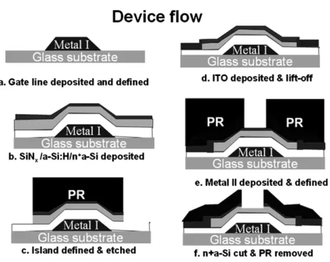
Fig. 1shows schematically the structure of the simple structure a-Si:H TFTs. After the gate electrode of 300 nm-thick MoW was patterned on the glass substrate, a 300 nm-thick silicon-nitride (SiNx) were deposited by plasma enhanced chemical vapor deposition (PECVD) method. The 100 nm-thick ITO was continuously deposited by sputtering and patterned as source/ drain electrodes. Finally, a 200 nm-thick a-Si:H active layer were deposited by PECVD method, and defined as the island region. Furthermore, the inverted-staggered a-Si:H TFTs with back-channel-etched (BCE) process, were fabricated on glass substrate for the study of electrical characteristics. The device fabrication process was described as followed. After the gate electrode of 300 nm-thick MoW was patterned on the glass substrate, the 300 thick silicon-nitride (SiNx), a 200 nm-thick a-Si:H active layer and a 50 nm-nm-thick n+-a-Si:H were continuously deposited by PECVD method. After defining the island region, the photo resist was not removed and the 100 nm-thick ITO was continuously deposited by sputtering. Afterward the lift-off process was used for the removal of photo resist and ITO in the island region. In general, the sputtering process of the ITO adds the oxygen for good ITO quality. Because the ITO deposition was prior to source/drain metal deposition, the contact resistance of the metal/ITO would be decreased. The capping ability of ITO was also confirmed by the scanning electron microscopy (SEM). The 300 nm-thickness MoW was deposited by sputtering and patterned as source/drain metal. After the electrodes are formed for devices, the n+-a-Si:H layer in the TFT channel region would to be etched off using the source/drain pattern as a mask. The detail process flow was illustrated inFig. 2. The dimension of channel length and width
Fig. 1. The structure of the simple TFTs.
both was 10 μm for the TFT devices. The electrical mea-surement was carried out by HP 4156C precision semiconduc-tor parameter analyzer. All TFT structures were measured under the back light illumination. The photo leakage current mea-surement was carried with the 3300 cd/m2CCFL back light to compare the difference in the off-state photo leakage currents between the proposed device and the conventional one. 3. Results and discussion
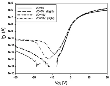
The photo leakage current of conventional a-Si:H TFTs was shown inFig. 3. When the a-Si:H TFT was operated in the small negative gate voltage (VGN−10 V) and 5 V drain
voltage, the photo leakage current is decreased with the increase of density of states (DOS), serving as recombi-nation centers. However, with the larger negative gate voltage (VGb−10 V), the large photo leakage current was observed.
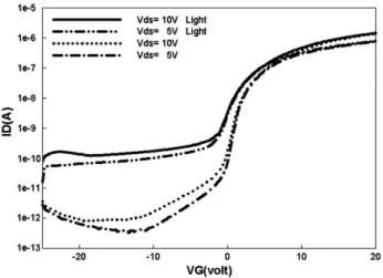
According to previous study [11], the larger off-state photo leakage current is due to the faster hole channel accumulation in the larger negative gate voltage.Fig. 4shows the electrical characteristic of the simple TFT structure. However, the photo
leakage current was saturated at about 10− 11A in the simple TFT structure. This characteristic was different from the conventional inverted-staggered a-Si:H TFTs. Because the ITO/a-Si:H device is a Schottky diode, the current is carried by majority carriers on both sides of the junction. The photocurrent is primarily due to the photo-excited electron-hole pairs in the a-Si:H, but also due to the photo-excited electrons from the conduction band of the ITO through the interfacial SiO layer into the conduction band of the a-Si:H. The photo-excited electrons in the a-Si:H are accelerated away from the interface and directly contribute to the photocurrent. Also, the photo-excited holes in the a-Si:H can contribute to the photocurrent by recombining via interface states with electrons from the ITO conduction band. However, these holes could also lead to photocurrent suppression via recombining with photo-excited electrons in the a-Si:H conduction band
[18]. The work function of the ITO is about 4.1 eV and the band gap of the ITO is about 3.7 eV. Because the off-state current under the back illumination is resulted from the hole generation in the a-Si:H layer, the barrier height for hole is the most important parameter to reduce the photo leakage current. The barrier height for hole is estimated about 3 eV according to the band diagram of ITO/a-Si:H structure. The holes were accumulated near the interface and recombined with photo-excited electrons. If the interfacial SiO layer was thick enough, the photo-excited holes in the a-Si:H can no longer tunnel through the SiO, and recombine with electrons in the ITO conduction band. Instead, they accumulated near the interface and recombined with photo-excited electrons. The photocurrent was, therefore, suppressed in the ITO/a-Si:H structure. Since the recombination rate near the SiO/a-Si:H interface is proportional to the concentration of holes trapped in this region, the simple structure a-Si:H TFT has showed the saturated photo leakage current characteristic. For the application of conventional inverted-staggered BCE a-Si:H TFTs, the ITO source/drain barrier height was introduced by
Fig. 3. The photo leakage current characteristic of conventional a-Si:H TFTs.
Fig. 4. The photo leakage current characteristic of the simple TFT structure.
Fig. 5. The characteristics and the device parameter of the a-Si:H TFTs with ITO as source/drain barrier.
the ITO lift-off process, as shown inFig. 2. After the device manufacture process, the characteristics of the a-Si:H TFTs with ITO as source/drain barrier demonstrated the field-effect mobility about 0.37 cm2/V-s, the minimum subthreshold swing about 0.83 V/dec, and the ION/IOFFratio is 106at VDS= 10 V. The
threshold voltage was about 2.02 V, determined from turn-on current (Ion) extrapolation in the linear region of ID–VGcurve at
VDS= 0.1 V, as shown in Fig. 5.Fig. 6shows the SEM of the
291 nm-thick thin film capping with 100 nm-thick ITO at the taper angle about 84.7°. The good capping ability of ITO also ensured the existence of the ITO/a-Si:H interface. Fig. 7
shows the transfer characteristics of the a-Si:H TFT with ITO as source/drain barrier under back light illumination. Here the source/drain is illuminated, and different drain voltages were tested. The photo leakage current of the a-Si:H TFT with ITO as source/drain barrier has shown the similar characteristic with the simple structure TFT. Furthermore, the photo leakage current is proportional to the drain voltage, and independent of gate voltage. That's also because the photo-excited holes in the a-Si:H accumulated near the interface and recombined with photo-excited electrons, thereby making the photocurrent characteristic different from the conventional a-Si:H TFT
without ITO as source/drain barrier. Besides, the reliability of the proposed device structure also showed inFig. 8. The gate bias stress condition was set Vg = 20 V, VD= VS is commonly
ground for 3600 s. After the gate bias stress, the shift of threshold voltage was only 2.2 V in the proposed structure. This result is also similar to the conventional a-Si:H TFT. Furthermore, the ITO capping process was not an additional step due to the necessity of having ITO as pixel electrode in conventional TFT-LCD manufacture.
4. Conclusion
We have fabricated the simple TFT structure to verify the photo leakage current of the ITO/a-Si:H device. The photo leakage current was different from the conventional inverted-staggered a-Si:H TFT. The suppression of the photocurrent was due to the holes accumulated near the interface and recombined with photo-excited electrons. Furthermore, the a-Si:H TFTs using the ITO as source/drain barrier via the lift-off process was also fabricated without increasing the process steps. The a-Si:H TFT with the ITO as source/drain barrier has shown superior characteristics of photo leakage current compared to conven-tional a-Si:H TFTs. The photo leakage current is suppressed by the source/drain barrier between the ITO/a-Si:H, and propor-tional to the drain voltage. The impact of using ITO layer for driving current is to effectively reduce the off-state current under the back illumination. Therefore, the off-state signal loss resulted from the a-Si:H TFTs photo leakage current was reduced. These results indicated that a-Si:H TFT with the ITO as source/drain barrier has the potential for the application of high quality TFT-LCD.
Acknowledgements
This work was partially supported by National Science Council, the Republic of China under contract Nos.NSC-94-2120-M-110-005, NSC94-2215-E-009-031, NSC-95-2120-M-110-003, NSC 95-2221-E-009-254-MY2, and MOEATechnology Development for Academia under Project 94-EC-17-A-07-S1-046 and MOE ATU Program.
Fig. 6. The SEM picture of the 291 nm-thick thin film capping with 100 nm-thick ITO at the taper angle about 84.7°.
Fig. 7. The transfer characteristics of the a-Si:H TFT with ITO as source/drain barrier under back light illumination.
Fig. 8. The transfer characteristics of the proposed device structure after the gate bias stressing for 1000, 2000, 3000, 3600 s.
References
[1] F.B. Ellis Jr., R.G. Gordon, W. Paul, B.G. Yacobi, J. Appl. Phys. 55 (1984) 4309.
[2] R. Baeuerle, J. Baumbach, E. Lueder, J. Siegordner, SID'99 Digest, Society of Information Display, 1999, p. 14.
[3] W.E. Howard, J. Soc. Inf. Disp. 3 (1995) 127. [4] S. Venkatesan, et al., IEDM Tech. Dig. (1997) 769. [5] D. Edelstein, et al., IEDM Tech. Dig. (1997) 773.
[6] K. Ono, Y. Imajo, I. Mori, R. Oke, S. Kato, K. Endo, H. Ishino, SID'05 DIGEST, 2005, p. 1848.
[7] Y. Yoshida, Y. Kikuchi, S. Daly, M. Sugino, SID'05 DIGEST, 2005, p. 1852. [8] J.K. Yoon, Y.H. Jang, B.K. Kim, H.S. Choi, B.C. Ahn, C. Lee, J.
Non-Cryst. Solids 164–166 (1993) 747.
[9] M. Akiyama, T. Kiyota, Y. Ikeda, T. Koizumi, M. Ikeda, K. Suzuki, SID '95 Digest, Society for Information Display, Florida, 1995, p. 158. [10] N. Hirano, N. Ikeda, H. Yamaguchi, S. Nishida, Y. Hirai, S. Kaneko, IDRC
'94 Digest, International Display Research Conference, CA, 1994, p. 369. [11] W.E. Spear, J. Non-Cryst. Solids 59/60 (1983) 1.
[12] J.N. Bullock, S. Wagner, Mater. Res. Soc. Symp. Proc. 336 (1994) 97. [13] T. Oshima, K. Tamaguchi, A. Yamada, M. Koganai, K. Takahashi, Mater.
Res. Soc. Symp. Proc. 336 (1994) 91.
[14] M. Nakata, S. Wagner, Appl. Phys. Lett. 65 (1991) 1940.
[15] J.S. Byun, H.B. Jeon, K.H. Lee, J. Jang, Appl. Phys. Lett. 67 (1995) 3786. [16] K.S. Lee, J.H. Choi, S.K. Kim, H.B. Jeon, J. Jang, Appl. Phys. Lett. 69 (16)
(1996) 2403.
[17] J.H. Choi, C.S. Kim, S.K. Kim, J. Jang, J. Appl. Phys. 82 (8) (1997) 4081. [18] R.L. Anderson, Appl. Phys. Lett. 27 (1975) 691.