Time-resolved spin filtering in semiconductor symmetric resonant barrier structures
Leo Yu and O. Voskoboynikov
Citation: Journal of Applied Physics 98, 023716 (2005); doi: 10.1063/1.1994945
View online: http://dx.doi.org/10.1063/1.1994945
View Table of Contents: http://scitation.aip.org/content/aip/journal/jap/98/2?ver=pdfcov Published by the AIP Publishing
Articles you may be interested in
Magnetotunneling in resonant tunneling structures with spinorbit interaction J. Appl. Phys. 110, 064507 (2011); 10.1063/1.3633252
Spin-dependent dwell times of electron tunneling through double- and triple-barrier structures J. Appl. Phys. 103, 083701 (2008); 10.1063/1.2904869
Spin filtering in an electromagnetic structure
J. Appl. Phys. 95, 7252 (2004); 10.1063/1.1652414
Spin-filter devices based on resonant tunneling antisymmetrical magnetic/semiconductor hybrid structures Appl. Phys. Lett. 84, 1955 (2004); 10.1063/1.1655688
Comment on “Strong wave-vector filtering and nearly 100% spin polarization through resonant tunneling antisymmetrical magnetic structure” [Appl. Phys. Lett. 81, 691 (2002)]
Appl. Phys. Lett. 82, 3570 (2003); 10.1063/1.1577821
Time-resolved spin filtering in semiconductor symmetric resonant
barrier structures
Leo Yua兲 and O. Voskoboynikov
National Chiao Tung University, 1001 Ta Hsueh Road, Hsinchu 300, Taiwan, Republic of China 共Received 16 July 2004; accepted 14 June 2005; published online 29 July 2005兲
Spin-dependent tunneling in semiconductor symmetric double barrier structures is studied theoretically. Our calculation is based on the effective one-band Hamiltonian and Dresselhaus spin-orbit coupling. We demonstrate that the ratio of the tunneling times of electrons with opposite spin orientations can vary over a few orders in magnitude. The large and tunable ratio of the tunneling times can serve as the basis in the development of all-semiconductor dynamic spin filters. © 2005 American Institute of Physics.关DOI: 10.1063/1.1994945兴
I. INTRODUCTION
Since the spin-dependent electronic device was proposed by Datta and Das,1the utilization of the spin-orbit coupling has been one of the key topics of semiconductor spintronics. However, a most elementary issue, an efficient means to ob-tain spin-polarized currents in semiconductor structures, has not been resolved yet. The conductivity mismatch between metals and semiconductors impedes the electron transport and makes the injection of spin-polarized electronic currents from strongly magnetized metals inefficient, as Schmidt
et al.2 pointed out. The reported experimental results on the polarization efficiency in metal-semiconductor junctions are less than 1%.3On the other hand, the spin-orbit interaction in semiconductors lifts the spin degeneracy of electrons’ energy and results in spin-dependent transport through semiconduc-tor junctions.
The spin-orbit interaction of electrons in III-V semicon-ductor materials is usually described by two contributions to the effective one-band spin-dependent Hamiltonian. One, of-ten referred to as the Rashba term, is induced by the inver-sion asymmetry of the macroscopic potential,4which can be controlled by external electric-field or material growth tech-niques. The other, referred to as the Dresselhaus term,5is due to the inversion asymmetry of the zinc-blende lattice. The interplay between these two terms has been studied by de Andrada e Silva,6showing that for narrow-gap semiconduc-tors, the contribution from the Rashba term to the spin-orbit interaction dominates over that from the Dresselhaus term. Hence the Dresselhaus term is often neglected. Calculations based on the Rashba spin-orbit interaction in III-V semicon-ductor heterostructures have been performed,7–12 showing the all-semiconductor tunneling structures can be a feasible means to obtain electronic spin-polarized currents. However, it was suggested recently11,13,14 that even through a single symmetric barrier, where the contribution from the Rashba term cancels out due to macroscopic symmetry,7 electrons can tunnel highly spin-polarized because of the Dresselhaus term.
In this paper we elaborate on this idea and evaluate the
spin-dependent tunneling 共delay兲 time in a symmetric reso-nant tunneling structure. The tunneling time is an important quantity in a tunneling process that determines the dynamic working range of tunneling devices. In this work we take the “stationary phase approach” to define the tunneling time, as taken by Bohm15 and Voskoboynikov et al.16 Our following discussion will reveal that when the spin-orbit interaction effect comes into play, the ratio of the tunneling time be-tween differently spin-polarized electrons can gain a few or-ders of magnitude. This provides the theoretical basis for time-resolved spin filtering. We also suggest that one can manipulate the tunneling time to a great variety by changing the barrier width. The relation between the delay time and the width is simple and can be used as a rule to select work-ing frequencies.
This paper is organized as follows. In Sec. II we detail our calculation of the electron spin-dependent transmission amplitude, of polarization efficiency, and of tunneling time. In Sec. III, the results of calculations for InGaAs/ InAlAs/ InGaAs double barrier tunnel structure are presented. In Sec. IV we summarize the results.
II. POLARIZATION EFFICIENCY AND TUNNELING TIME
We consider the spin-dependent tunneling process through a symmetric double barrier structure grown along the z储关001兴 direction, as shown in Fig. 1共a兲. Taking the sta-tionary phase approach the tunneling time is described to be the phase delay time, which is the energy derivative of the phase⍜ of the transmission amplitude16
=ប⌰
Ez
, 共1兲
where⍜±= arg兩t±兩, Ezdenotes the longitudinal component of
the electron’s energy共corresponding to a motion parallel to the heterostructure growth direction兲, and= ± 1 refers to the spin polarization.
Our calculation is performed on the basis of the effective electronic one-band Hamiltonian, energy- and position-dependent electron effective mass approximation, and the Ben Daniel–Duke boundary conditions.17 The layers of the structure are perpendicular to the z axis and the in-plane a兲Electronic mail: [email protected]
0021-8979/2005/98共2兲/023716/5/$22.50 98, 023716-1 © 2005 American Institute of Physics
electron’s wave vector is k. With the above assumptions the electronic wave function in the jth region can be presented as ⌽共x,y,z兲 =j共z兲exp关i共kxx + kyy兲兴, 共2兲
where k =
冑
kx2 + ky
2
and⌿j共z兲 satisfies the z component of the
Schrödinger equation
Hˆjj共z兲 = E⌿j共z兲, 共3兲
with the spin-dependent Hamiltonian in each region,13
Hˆj= Hˆj0+ HˆjSO. 共4兲
In Eq.共4兲 Hj0is the Hamiltonian of the system without
spin-orbit interaction, Hˆj0= − ប2 2mj共E兲
冉
d2 dz2− k 2冊
+ E jc, and 1 mj共E兲 =2P 2 3ប2冋
2 E − Ejc+ Ejg + 1 E − Ejc+ Ejg+⌬j册
共5兲 presents the energy- and position-dependent reciprocal effec-tive mass. Ejc, Ejg, and ⌬j stand for the position-dependentconduction-band edge, band gap, and the spin-orbit splitting in the valence band. P is the momentum matrix element.17In Eq. 共4兲 HˆjSOis the spin-dependent part of the Hamiltonian
which originates from the Dresselhaus term 共in the sym-metrical structure the Rashba spin-orbit coupling vanishes7兲. When the kinetic energy of electrons is substantially smaller
than the barrier’s height we can present this term as the following:13
HˆjSO=␥j共ˆxkx−ˆyky兲
d2
dz2, 共6兲
whereˆxandˆy are the corresponding x and y components
of the vector of the Pauli matricesˆ =兵ˆx,ˆy,ˆz其 and␥jis a
material constant of the jth region.
The boundary conditions for the solution ⌿j共z兲 at the
interface between the j and j + 1 regions have been intro-duced in Ref. 17, 1 mj共E兲
冋
d dz⌿j共z兲册
z=zj = 1 mj+1共E兲冋
d dz⌿j+1共z兲册
z=zj , ⌿j共zj兲 = ⌿j+1共zj兲. 共7兲To diagonalize the Hamiltonian one can put the in-plane wave vector k along the x direction 共ky= 0兲 and take the
electronic wave functions to be ⌿j±共z兲 =j±共z兲
冉
1 ⫿1
冊
, which are eigenfunctions of ˆx.The general solution of Eq.共3兲 in a given jth region has the form j共z兲 = ajj +共z兲 + b jj −共z兲, where j
±共z兲 is a pair of linearly independent solutions of Eq. 共3兲 within that region. In the regions j=1,3,5 the solu-tions are the following plane wave sets:
±j共z兲 = exp共±ikjz兲, where kj共Ez,k兲 =⌺j ប
冑
2mj共Ez,k兲共Ez+ E1c− Ejc兲 − ប2冋
1 − mj共Ez,k兲 m1共Ez,k兲册
k2, ⌺j=冑
1 + 2␥jmj共Ez,k兲 ប2 k,and Ez is the longitudinal component of the total energy in
the first region,
E = E1c+ Ez+
ប2k2 2m1共Ez,k兲
.
We use this expression, along with Eq. 共5兲, to find the de-pendence of mj共Ez, k兲 on E共Ez, k兲共j=1–5兲. In the regions j
= 2 , 4 the solutions are chosen to be
j
±共z兲 = exp共±q
jz兲,
where
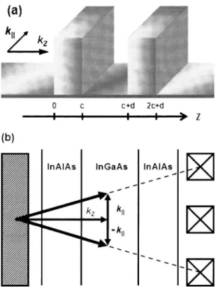
FIG. 1.共a兲 Sketch of electron tunneling with the wave vector 共k,kz兲, where
k is the in-plane wave vector and z储关001兴 the direction of the structure
growth. The variation of the band parameters forms a symmetric double barrier tunneling heterostructure.共b兲 A schematic illustration of a possible spin-filter implementation.
023716-2 L. Yu and O. Voskoboynikov J. Appl. Phys. 98, 023716共2005兲
qj共Ez,k兲 =⌺j ប
冑
2mj共Ez,k兲共Ejc− E1c− Ez兲 + ប2冋
1 − m2共Ez,k兲 m1共Ez,k兲册
k2. The coefficients兵aj, bj其 are to be determined from theboundary conditions in Eq. 共7兲. The sets of coefficients in neighboring regions are related by the transfer matrix M:18
冉
ajbj
冊
= Mj
冉
aj+1bj+1
冊
.
According to the boundary conditions in Eq. 共7兲 the matrix
Mj is written as7 Mj = 1 ⌬j
冉
⌳j+ − ⌳ j+ + −⌳j−− −⌳j−−冊
, with ⌬j=⌬j + −⌬j − , ⌬j ± =再
d dzln关j ±共z兲兴冎
z=zj ⌳j+ ± =冉
mj mj+1 ⌬j ± −⌬j +冊
⫿j+1共zj兲 +j共zj兲 , ⌳j−± =冉
mj mj+1 ⌬±j−⌬−j冊
⫿j+1共zj兲 j +共z j兲 .The double barrier tunneling structure consists of four inter-faces, so the total transfer matrix is written as
M=兿j=14 Mj.
Electrons are injected from the region of j = 1. The transmit-ted waves will appear in the region of j = 5. With this as-sumption the transmission amplitude is given by
t= 1 共M兲11,
and the spin-dependent delay time is written as
共Ez,k兲 = − ប
arg关共M兲11兴
Ez
.
The polarization efficiency of the structure was defined in Ref. 7 to be
P =兩t+兩
2−兩t−兩2 兩t+兩2+兩t−兩2.
III. CALCULATION RESULTS
In Fig. 2 we demonstrate the numerical results of the polarization efficiency P of an electron’s tunneling through a resonant symmetric structure made of In0.53Ga0.47As/ In0.52Al0.48As heterojunctions. All calculations are performed within a region on the共Ez, k兲 plane where the total energy of
electrons is substantially smaller than the barrier’s height 关see Eq. 共6兲兴. The numerical values of␥in different materials are obtained for InAs and GaAs from Ref. 13, for AlAs from Ref. 21, and for alloys with the Vegard’s superposition law in Ref. 22. One can see that the polarization efficiency shows
typical resonant behaviors as a function of the longitudinal energy and in-plane wave number. The peaks correspond to the spin-split lowest resonant levels on the共Ez, k兲 plane. The
splitting of the resonant levels results in an abrupt change of the sign of the polarization efficiency.
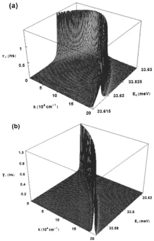
The delay time of tunneling electrons with two opposite spin polarizations is presented in Fig. 3. The position of the peak corresponds to the resonant tunneling level, at which the tunneling electron is “trapped” in the quasibound states of the well. Although the positions of the peak for the two opposite spin polarizations do not seem to have the same functional dependence on共Ez, k兲, the distance between them
in Ezis proportional to k, in accordance to the linear
depen-dence on k of the Dresselhaus spin spliting of the levels in the well.
Since the positions of the peaks depend sharply on Ez
and k, we present in a logarithmic scale the ratio of the delay time between oppositely spin-polarized electrons 共see Fig. 4兲. This ratio increases with the length of k and can gain a few orders in magnitude.
The ratio of the delay times can be tuned by means of structural design. For this reason we present in Fig. 5 the dependence of the maximal delay time on the barrier thick-ness c and the well width d. The delay time increases with increasing c and d, but has different functional dependencies on each of them. From the calculation results presented in Fig. 5 for +, one can approximate the dependencies as the following formula:
+⬀ d2exp共␣c兲,
where␣is a constant; for −of the same structure, one can recalculate it from the logarithmic ratio. For our symmetric InGaAs/ InAlAs/ InGaAs double barrier structure ␣⬇0.074 when d = 18 nm. Applying this formula one can determine
FIG. 2. Polarization efficiency P calculated for an In0.53Ga0.47As/ In0.52Al0.48As/ In0.53Ga0.47As DBT structure共see Fig. 1兲. The
structure parameters are obtained in Ref. 20: E1g= 0.418 eV, E2g= 1.52 eV, ⌬1= 0.38 eV, ⌬2= 0.341 eV, m1共0兲=0.044m0, m2共0兲=0.084m0 共m0 is the
free-electron mass兲, ␥1= 0.076 9 eV nm3 共Ref. 13兲, ␥2= 0.073 4 eV nm3
共Ref. 21兲, c=6 nm, and d=12 nm.
the actual region of frequencies where the structure is appli-cable to spin-dependent electronic devices.
The large and tunable ratio of spin-dependent delay times in symmetric structures provides a new method to per-form spin filtering. Once we have clear spin-distinguishable times of the tunneling processes, the cutoff frequencies of electrons differently spin polarized will also split. By select-ing an appropriate region of frequency, the current contribu-tion from electrons with a lower cutoff frequency can be
greatly suppressed. In this sense we achieved time-resolved spin filtering. This dynamic regime is more efficient than the conventional static regime. Indeed, in the static regime the means to spin filtering is a large spin splitting of resonant levels in the well,9which requires a large transversal dc bias 共or built-in electric field兲. In symmetrical structures instead one can perform the dynamic spin filtering even when only a weak time-dependent signal is applied. We mention by pass that the spin-relaxation processes can also be suppressed by the same means.
An important point that tends to be missed is the fact that the spin filtering based on the spin-orbit coupling re-quires a control of the electrons’ in-plane momentum.9,11,12 Figure 1共b兲 illustrates schematically the basic concept of a dynamic spin filter fabricated in a split multicollector con-figuration. The in-plane momentum control of electrons and the dynamic spin filtering are achieved by sending a series of high-frequency voltage pulses to different leads of the mul-ticollector. Another method to control the electrons’ in-plane momentum was demonstrated recently with side-gated reso-nant devices in a dc regime.12
IV. CONCLUSIONS
Based on the stationary phase concept and the effective one-band Hamiltonian with the Dresselhaus spin-orbit cou-pling, we present the numerical results of the tunneling time through a realistic InGaAs/ InAlAs/ InGaAs resonant sym-metric structure. It is shown that the polarization efficiency of the structure has a well-defined resonance behavior, which leads to a considerable spin polarization of electrons tunnel-ing through. In the lower-energy region, the ratio between the tunneling times of electrons with opposite spin orienta-tions can vary over a few orders in magnitude. The results indicate that the Dresselhaus spin-orbit coupling separates the time-dependent response of differently spin-polarized tunneling electrons. Furthermore, the large and tunable ratio of the tunneling times provides a possible way to construct a dynamic spin filter. The characteristic time of such devices also has been estimated and presented, showing simple func-tional dependencies on the barrier thickness and the well width. The dependencies can be exploited to design spin-tronic devices working in the desired frequencies.
FIG. 3. The delay time for the structure in Fig. 2.共a兲 Delay time for elec-trons with spin “up.”共b兲 Delay time for electrons with spin “down.”
FIG. 4. Ratio between the delay time for different polarizations of the elec-tron spin. The structure is the same as in Fig. 2.
FIG. 5. The variation of the maximum delay time with respect to共a兲 the barrier thickness and共b兲 the well width. The constant0= 10−12s is defined
for normalization. The structure is the same as in Fig. 2.
023716-4 L. Yu and O. Voskoboynikov J. Appl. Phys. 98, 023716共2005兲
This work was supported by the National Science Coun-cil of R.O.C. under Contract No. NSC 93-2112-M-009-008.
1S. Datta and B. Das, Appl. Phys. Lett. 89, 665共1990兲.
2G. Schmidt, D. Ferrand, L. W. Molenkamp, A. T. Filip, and J. van Wees,
Phys. Rev. B 62, R4790共2000兲.
3P. R. Hammar, B. R. Bennett, M. J. Yang, and M. Johnson, Phys. Rev.
Lett. 83, 203共1999兲; S. Gardelis, C. G. Smith, C. H. W. Barnes, E. H. Linfield, and D. A. Ritchie, Phys. Rev. B 60, 7764共1999兲; Semiconductor
Spintronics and Quantum Computation, edited by D. D. Awschalom, D.
Loss, and N. Samarth共Springer, Berlin, 2002兲.
4Yu. A. Bychkov and E. I. Rashba, J. Phys. C 17, 6039共1984兲. 5G. Dresselhaus, Phys. Rev. 100, 580共1955兲.
6E. A. de Andrada e Silva, Phys. Rev. B 46, 1921共1992兲; E. A. de Andrada
e Silva and G. C. La Rocca, ibid. 50, 8523共1994兲.
7A. Voskoboynikov, S. S. Liu, and C. P. Lee, Phys. Rev. B 59, 12514
共1999兲.
8E. A. de Andrada e Silva and G. C. La Rocca, Phys. Rev. B 59, 015583
共1999兲.
9A. Voskoboynikov, S. S. Liu, and C. P. Lee, J. Appl. Phys. 87, 387共2000兲. 10T. Koga, J. Nita, H. Takayanagi, and S. Datta, Phys. Rev. Lett. 88, 126601
共2002兲.
11Z.-Y. Ting, D. X. Cartoixá, D. H. Chow, J. S. Moon, D. L. Smith, T. C.
McGill, and J. N. Schulman, Proc. IEEE 91, 741共2003兲.
12J. S. Moon, D. H. Chow, J. N. Schulman, P. Deelman, J. J. Zinck, and D.
Z.-Y. Ting, Appl. Phys. Lett. 85, 678共2004兲.
13V. I. Perel’, S. A. Tarasenko, I. N. Yassievich, S. D. Ganichev, V. V.
Bel’kov, and W. Prettl, Phys. Rev. B 67, 201304共2003兲.
14D. Z.-Y. Ting and X. Cartoixà, Phys. Rev. B 68, 235320共2003兲. 15D. Bohm, Quantum Theory共Prentice-Hall, New York, 1951兲; M. Buttiker
and R. Landauer, Phys. Rev. Lett. 49, 1739共1982兲; D. Dragonman and M. Dragonman, IEEE J. Quantum Electron. 32, 1932 共1996兲; G. Garcia-Calderon and A. Rubio, Phys. Rev. A 55, 3361共1997兲; J. U. Kim and H. H. Lee, J. Appl. Phys. 84, 907共1998兲.
16O. Voskoboynikov, S. S. Liu, and C. P. Lee, Solid State Commun. 155,
477共2000兲.
17G. Bastard, Wave Mechanics Applied to Semiconductor Heterostructures
共Les Edition de Physique, Les Ulis, 1990兲.
18E. O. Kane, Tunneling Phenomenon in Solids共Plenum, New York, 1969兲. 20J. H. Davies, The Physics of Low-dimensional Semiconductors: An
Intro-duction共Cambridge University Press, Cambridge, 1998兲.
21R. Eppenga and M. F. H. Schuurmans, Phys. Rev. B 37, 10923共1988兲. 22J. Singh, Electronics and Optoelectronic Properties of Semiconductor
Structures共Cambridge University Press, Cambridge, 2003兲.