Optimised integrated CMOS optical receiver for
optical interconnects
Y.-T. Huang
Indexing terms: Optical interconnects, CMOS optical receivers
Abstract: The optimisation of an optical receiver is discussed and transient charcteristics of two basic simple integrated receivers in CMOS systems are analysed and compared in detail. In analysis, a maximum current parameter is devel- oped and used for optimisation design. Among these two receivers, the low-impedance config- uration is presented for high-speed operation. SPICE simulation and preliminary experimental results with discrete devices are also illustrated and discussed.
1 Introduction
Since optical interconnects was suggested as a method to improve the performance of VLSI systems [ 1-1 11, many researchers have investigated its application in CMOS systems [12-18,211. Bergman er al. started to use a
simple receiver with a saturation PMOS load to imple- ment optical interconnects in a CMOS VLSI system [13, 15, 161. However, the long switching fall time of this receiver significantly limited the operation speed of the system. Although the simulation evaluation for this receiver was reported and two other different receivers with two more devices were presented to improve the switching speed by Wu et al. [17], the detailed analysis of transient characteristics of these receivers were not dis- cussed and the long-tail problem of the switching wave- form was still not efficiently improved. One of these two receivers gave a long switching fall time, and the other gave a smaller output logic swing and consumed more power. Some improvements were presented by Chou et
al. [18] although a detailed analysis and optimisation of
this receiver design were not discussed. As will be shown, optimisation is necessary to achieve high-speed oper- ation.
In addition to high speed and large output swing con- siderations, another important aspect for optical inter- connects is to minimise optical receiver complexity for practical applications in compatible CMOS technologies. In this paper, we first discuss the basic integrated CMOS optical receiver, a very simple structure which only con- tains one photodetector and one biasing load device, and the concept for optimising this circuit. Two different con- figurations, a saturation load and a low-impedance load, 0 IEE, 1993
Paper 9 1 8 9 (E3, E13), first received 3rd February and in revised form 8th September 1992
The author is with the Department of Electronics Engineering and Institute of Electronics, National Chiao Tung University, Hsinchu, Taiwan, Republic of China
IEE PROCEEDINGS-J, Vol. 140, No. 2, APRIL 1993
are then discussed. The transient characteristics of these configurations are analysed and compared in detail. The low-impedance configuration is presented for high-speed optical interconnect applications and an optimised design is proposed. Analytical results and SPICE simulations for typical examples are also provided. Finally, preliminary experimental results with discrete devices are given and conclusions are summarised.
2
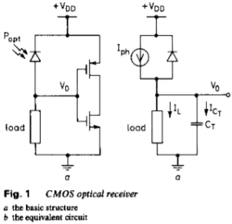
The structure of a basic CMOS optical receiver without any gain stage is shown in Fig. 1. VDD is the supply
Basic integrated CMOS optical receiver
a a
Fig. 1 CMOS optical receiver a the basic structure
b the equivalent circuit
voltage, V , is the output voltage, C , represents the total
effective capacitance (which includes CMOS inverter input capacitance C i , the detector capacitance Cdn and the biasing load device output capacitance
CO),
I, is the photocurrent of the detector during an illumination pulse, I, is the load current, and IcT is the capacitor charging current. This structure only contains one photo- detector and one biasing load device to provide a desired output logic swing. The rise and fall times, and output logic swing are functions of the type and the effective resistance of the biasing load. When a light pulse illum- inates the detector, a photocurrent Ipk is generated andThe author would like to thank Prof. R.K. Kostuk at the University of Arizona for his helpful dis- cussions, and to acknowledge the National Science Council of the Republic of China for sup- porting this research under contract NSC 80- 0404-E-009-26.
divided between I, and
I,. .
Therefore, the capacitor charging current I C . becomes I,, - I,. A small load resistance with large I , decreases I,, , and requires a long rise time to charge the capacitor to a desired voltage level. On the other hand, when the light is turned off, no photocurrent is generated and the load current I , dis- charges the capacitor. A smaller load will have a higher discharging currentI I,. I
and a shorter fall time. By suit- ably adjusting the effective load resistance, the average capacitor charging and discharging currents can be equalised, providing a symmetric signal waveform with equal rise and fall times. In this case, the total switching time, which is the sum of the rise and fall times, is mini- mised and the functional signal frequency is maximised In addition to the symmetric waveform, another con- sideration for a signal is a large output swing, which pro- vides good noise immunity and fast switching response of the receiving inverter. If we use a linear passive resistor as the biasing load, to have a full logic swing, the resistance value is given by R = VDD/Iph. For a 40% efficient integ- rated detector with 0.5mW optical input power at 780 nm wavelength, and a typical V,, of 5 V, the photo- current I,, is 0.126 mA and the required resistance for a full-swing output is approximately 40 k 0 . In an integ- rated circuit, a resistor of this value requires a large frac- tion of the limited area and is not appropriate. We use an enhancement-mode nMOS transistor in a standard CMOS process as the biasing load to provide a nonlinear resistance characteristic. Using this device as the biasing load, the receiver has two different configurations : one is connecting the gate of this nMOS transistor to the drain output, i.e. V,, = V,, = V, (a similar structure has been used and briefly discussed in References 13, 15 and 16), and the other is connecting the gate to the most positive potential V,, , i.e. V,, = V,,.
In the subsequent discussions, V,, is defined as the low steady-state output voltage and VOH as the high steady- state out-put voltage. To analyse the transient character- istics of these circuits, a maximum-current parameter m is defined as the ratio of the photocurrent I p h to the maximum transistor current I,S(V,, = V,,), which is ~191.
where iDJVG, = V,,) is the drain saturation current for a gate bias of V,, and the maximum current of this tran- sistor (neglecting small geometry effects), which is given by
ID,( VGs = V,,) = k (”’
where k is the transconductance parameter and V, is the
threshold voltage. A normalisation time, T , is defined as (3)
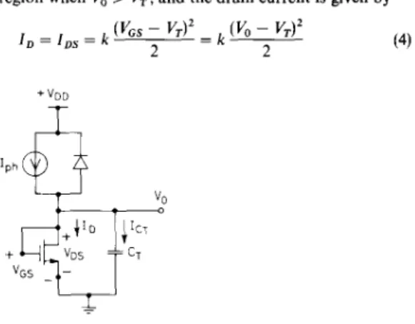
3 Transient analysis and optimal design 3.1 Saturation CMOS optical receiver ( V G s = V D s )
The equivalent circuit of the first configuration men- tioned above is shown in Fig. 2, where V,, , VGs, and 1,
are the drain bias, gate bias, and drain current of the nMOS load transistor, respectively. For this config- uration V,, = V,, = V, and the drain saturation voltage is given by V,,, = V,, - V , = V,, - V T . With an
108
enhancement-mode nMOS transistor (V, > 0), V’, > VDss, therefore the transistor operates in the saturation region when V, V, , and the drain current is given by
(4)
z
+q%$
“GS - --
Fig. 2 Saturation C M O S optical receiver (V,, = V,)
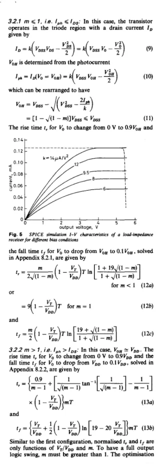
where I,, is the drain saturation current of the nMOS load transistor. The output capacitance of the transistor includes the gate-substrate capacitance (C,J and drain- substrate capacitance (Cds). Typical current-voltage char- acteristics of this saturation structure are shown in Fig. 3.
I I I L
- 3 4 5 6
output voltage, V Fig. 3
for different bias conditions
SPICE simulation I-V characteristics of a saturation receiver
When the light is off, V,, is V,, since the output cannot be discharged to a value lower than the threshold voltage. When the light is on, I,, is generated and V,, is determined by the value of m, which will be discussed below.
3.7 .I m
<
7 , i.e. I,,,<
/& In this case,and
= vT
+
J ( m ) ( v D D - vT)<
vDD (6) The rise time t , for V, to change from V, to V,+
0.9(V0,- V,) and the fall time for Vo to drop from V,, to V,
+
0.1( V,, - V,), solved in Appendix 8.1.1, are given byt , =
JO
2 (1 - 2 ) T In 19 ( 7 4 IEE PROCEEDINGS-J, Vol. 140, N o . 2, A P R I L 1993and
t, = 9,/(m)( 1 -
2 ) T
3.1 2 m > 1 , i.e. I,, > IDS: In this case, V,, N V,,. The
rise time t, for V, to change from V, to V,
+
O.9(VD,-
V,) and the fall time for V, to drop from V,, to V,+
O.l(V,, - V,), solved in Appendix 8.1.2, are given byand
t,=9m
(
1--3
TUsing T
=
(V,JI,,&C, as the normalisation time, nor-malised t, and tf are only functions of VT/V,, and m. Due to the parabolic form of the transistor current in eqn. 8, the average discharging current at O F F state is much smaller than the average charging current at ON state, therefore the rise and fall times can not be equalised, and the fall time is much longer than the rise time, which can be seen from eqns. 7 and 8.
In summary, there are three disadvantages of the satu- ration load
CMOS
receiver :(i) the output offset voltage of the O F F state is V, (ii) the output capacitance of the biasing transistor (CO = C,
+
C
,
)
is much larger than the other config- uration to be considered(iii) the switching waveform has a long tail with a slow falling response which limits high-speed performance.
3 2 Low-impedance CMOS optical receiver
The equivalent circuit of a low-impedance CMOS receiver is shown in Fig. 4. In this configuration V,, =
( V G s = V D O )
+yF:
"GS - -Fig. 4 Low-impedance C M O S optical receiver (VGS = VDD)
V,, and V, = V', which biases the gate to the most posi- tive potential, and produces a low effective channel resist- ance. The drain saturation voltage VDss is therefore equal to VDSS = VD,
-
VT. The output capacitance of thebiasing transistor only includes the drain-substrate capacitance
(CA,
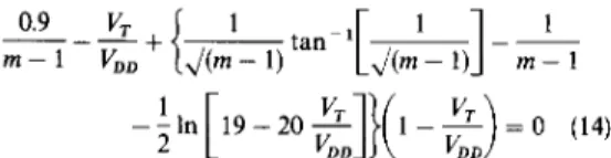
which is negligible compared with the gate-substrate capacitance (C,) [20]. Typical current- voltage characteristics of this low-impedance structure are shown in Fig. 5.When the light is off, V,, is 0 V. When the light is on, I, is generated and V,, is determined by the value of m, which will be discussed below.
IEE PROCEEDINGS-J, Vol. 140, N o . 2, APRIL 1993
3 2 . 1 m
<
1. i.e. I,,<
IDS: In this case, the transistor operates in the triode region with a drain current I ,given by
V,, is determined from the photocurrent
1, =
ZdV,
= Vo,) = k(
Vo, --
2 which can be rearranged to haveoutput voltage, V Fig. 5
receiver for different bias conditions
SPICE simulation I-V characteristics of a load-impedance
the fall time t , for V, to drop from V,, to 0.1 V,, , solved in Appendix 8.2.1, are given by
1
1+
1 9 4 ( 1 - m) 1+
J(1-
m) t, =-
2J(r-m)(1-2).In[
form < 1 (120) or = 9 1-- T f o r m = l(
3
and3.2.2 m > 1, i.e. I,,
>
IDS: In this case, V,, N V D D . The rise time t, for V, to change from 0 V to 0.9VDD and the fall time t , for V, to drop from V,, to 0.1 V,,,
solved in Appendix 8.2.2, are given byx (1 - 2 ) ) m T ( 1 3 4
and
Similar to the first configuration, normalised t, and t , are only functions of VT/V,, and m. To have a full output logic swing, m must be greater than 1. The optimisation 109
condition of equalising t , and tf gives the following rela- tion
2
- 5 l n[
19-20-3>(
I - -3
= O (14),
c /
,
,
When V,/V,, is given, the optimised m can be obtained from eqn. 14.
In an available CMOS process, the threshold voltage
VT and the minimum feature-size transconductance parameter k, of the biasing transistor are fixed. There- fore, an optimised m can be obtained for an operation
V,,, and the corresponding gate aspect ratio ( W / L ) for a specific I,, can be designed to achieve this desired m value from the following relation
where W and L are the gate width and channel length of the biasing transistor, respectively.
4
For given illumination and bias conditions, the output voltage and the switching times can be calculated from analytical results in Section 3. Using the supply voltage
V,, as the normalisation voltage, the normalised high
state voltage (V,,,/V,,) is only function of the maximum
current parameter m defined by eqn. 3, and is shown in Fig. 6 for m
<
l(V,,, c V,, for m > 1). Using TAnalytical. SPICE simulation results and design examples
impedance receiver has at least one order higher switch- ing speed.
We used SPICE to simulate our circuits and the results were in good agreement with our analysis. Figs. 8 and 9 show SPICE simulation examples of transient response for our saturation and low-impedance receivers
,
16t
/ / / / /,
0 C E L ' 0 0 4 0.8 1.2 1.6 2.0 maximum current parameter (m) Fig. 7~ nse time fall time
Analytic normalised response times for different bias Conditions
~~~~ /
L o t
I C I-E
,/-- g o H , I 1 I I,
,
1 I,
0 0.2 0 4 0 6 0 8 1 0 moximum-current parameter (m) Fig. 6 I,, , i.e. m<
IV,, CT/I,, in eqn. 7 as the normalisation time, normal-
ised rise and fall times are only functions of the normal- ised threshold voltage (VT/VDD) and the maximum current parameter m, and are shown in Fig. 7 with a typical value of 0.15 for VT/V,,. The results show that the fall time of a saturation configuration is always much longer than the rise time and the photocurrent is not efficiently utilised. For the low-impedance configuration, the rise and fall times can be equalised, which maximises the functional clock frequency. Making comparison of the normalised switching times between two configurations shown in Fig. 7, and also taking into account the additional output capacitance of the first configuration, the optimised low- Analytic normalised high steady-state output voltages for I,, d
110
'
0 5 10 15 20 25 30
time. n S Fig. 8
for dimerent bias conditions
SPICE simulation switching response of a saturation receiver
l t
O O k
I L
L E 12 16 20 time, ns
Fig. 9 SPICE simulation switching response of a low-impedance receiuerfor different bias conditions
with a typical 2 pm CMOS process: V,, = 5 V,
v,
=0.15VDD, k , = 56 pA/Vz, Ci = 16.6 fF, C,, = 4.16 fF,
cds = o,80 fF, and Cder is o,025 fF,pm~ (with Optical receivers were implemented with discrete com-
ponents to evaluate circuit characteristics. The threshold voltage V,, was set at 4 V to give a value of VT/VD, = 0.15 corresponding to the example in the previous dis-
5 Preliminary experimental results
1014 m - 3 epilayer doping concentration) 120, and
12.3 f F for a detector with 25 pm diameter, The detector "Itage vT Of the biasing transistor was o.6
v.
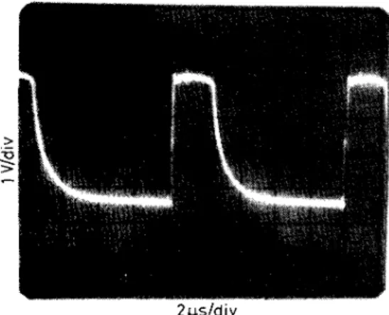
The efficiency qder can be expressed bytlder = - exp (-ad) (16) cussions. A typical switching response of -a saturation CMOS optical receiver is shown in Fig. 11. The low state and is about 40% in our examule. where lla is the lieht 1 I
penetration depth, which is 10 pm in silicon material ?or a 780nm wavelength, and d is the junction depletion depth. For a 0.5mW optical input power at 780nm wavelength, the photocurrent I,, is 0.126 mA. Corres- ponding parameter values are listed in Table 1. Fig. 8 shows that the logic swing of a saturation configuration is reduced by VT in the O F F state, and that the fall time is very long as discussed in Section 3.1. Fig. 9 shows that the rise and fall times of a low impedance configuration can be equalised, and the switching speed is one order of magnitude higher than a saturation configuration for full-swing output.
As indicated the low-impedance receiver is more suit- able for high-speed operation. Since the optimised m and the corresponding normalised time (T = t , = r,) of this configuration are only functions of VT/V,, (eqns. 13 and
14), we illustrate their relationships in Fig. 10 to provide
k2.0 21.7 z1.6
I t
1
2.0 2ps/divFig. 11 Experimental result o f a saturation C M O S optical receiuer is VT, which reduces the output logic swing by V,, and the switching waveform has a long tail with a long fall time of 4 ps as discussed in previous analytical results. Fig. 12 shows the switching response of an optimised low-impedance CMOS optical receiver. The result shows that the rise and fall times are equalised, and the photo-
able optical input power (Pop = 0.5 mW). Table 1 shows channel length provides this optimised biasing condition.
50 n s Id i v
that a transistor with 2 Pm gate width and 11.8 Pm Fig. 12 Experimental result of U low-impedance C M O S optical receiuer
Table 1 : Corresponding parameter values for different m
k. p A P 2 6.00 8.00 9.50 12.0 14.0 20.0 4 0 0 m 2.33 1.74 1.46 1.16 0.997 0.698 0.349 WIL 0.107 0.143 0.170 0.214 0.250 0.357 0.714 L. pm 18.7 14.0 11.8 9.3 8.0 5.6 2.8 Css, fF 38.8 29.1 24.5 18.7 16.6 11.6 5.8 Co,fF(V,,=Vo,) 39.6 29.9 25.3 19.5 17.4 12.4 6.6 C,.fF (V,,=Vo,) 68.5 58.8 54.2 48.4 46.3 41.3 35.5 Co. fF (V,,= VDD) 0.8 0.8 0.8 0.8 0.8 0.8 0.8 C,, fF (V,,= VDD) 29.7 29.7 29.7 29.7 29.7 29.7 29.7 W = 2 pm, ko=56pA/V2, VDD=5V. V,=O.75V. IP,=0.126mA; C,,=
1.04 fF/pm2, C,, = 0.20 fF/pm', C, = 16.6 fF, C,,, = 12.3 fF
Cd,, fF 0.8 0.8 0.8 0.8 0.8 0.8 0.8
current is efficiently utilised. The total effective capa- citance C , of this example is about 45 pF, the photocurrent I,! is 6 mA, and the response time ( t , and
t,) is 75 ns, which shows much faster switching speed than the saturation configuration shown in Fig. 11. Since the response time is proportional to VDD CT/I,,, project- ing these experimental results to an integrated receiver with a capacitance of 29.7fF and a photocurrent of 0.126mA as used in the analysis of Section 4, the response time is about 2.4 ns, which is close to the ana- lytical result. This result shows that the optimised integ- rated low-impedance receiver can operate at high rates with a reasonable optical input power ( P o p = 0.5 mW) c211.
6 Conclusions
In order to efficiently apply optical interconnects in an electronic computing system, a simplified optical receiver must be used. In a CMOS process, saturation and low- impedance configurations are two basic integrated optical receivers without any gain stage. The transient characteristics of these two receivers have been discussed in detail. A design parameter, maximum current param- eter m, which describes the relation between the photo- current of the detector and the maximum current of the biasing device was developed for analysis and design. The low-impedance receiver was presented for high-speed operation. This receiver when optimised provides a sym- metrical switching waveform with a full logic output voltage swing and efficiently utilities the available photo- current. This optimised receiver can operate at high- speed with a practical optical input powers (7 = 2.3 ns with P,, = 0.5 mW for 2 pm feature size). Preliminary experiments were performed with discrete devices and projected to integrated receivers by scaling capacitance values. The results verified the analytical and SPICE simulation predictions.
7 References
1 GOODMAN, J.W.: ’Optical interconnections in microelectronics‘, Proc. SPIE, 1984,456, pp. 72-85
2 GOODMAN, J.W., LEONBERGER, F.I., KUNG, S.Y., and ATHALE, R.A.: ‘Optical interconnections for VLSI systems‘, Proc. IEEE, July 1984,72, pp. 850-866
3 HUSAIN, A.: ‘Optical interconnect of digital integrated circuits and systems’, Proc. SPIE, Jan. 1984,466, pp. 10-20
4 HAUGEN, P.R., RYCHNOVSKY, S., HUSAIN, A., and HUT- CHESON, L.D.: ‘Optical interconnects for high speed computing’,
Opt. Eng., Oct. 1986,25, (lo), pp. 1076-1085
5 HARTMAN, D.H.: ‘Digital high speed interconnects: a study of the optical alternative’, Opt. Eng., Oct. 1986, 25, (IO), pp. 1086-1 102 6 TSANG, D.Z., SMYTHE, D.L., CHU, A., and LAMBERT, J.J.: ‘A
technology for optical interconnections based on multichip integra- tion’, Opt. Eng., Oct. 1986, 25,(10), pp. 1127-1131
7 HARTMAN, D.H.: ‘Optical interconnection technology in the tele- communications network. IEEE Proceedings of the Fall Joint Com- puter Conference, Dallas, Texas, Nov. 1986, pp. 461-478
8 SMITH, P.W.: ‘On the role of photonic switching in future communications system’s’, IEEE Circuits and Devices, May 1987. 3, (31, PP. 9-14
9 HINTON, H.S.: ’Photonic switching technology applications’, AT&T Techn. J., May/June 1987,66, (3), pp. 41-53
10 HORNAK, L.A., and TEWKSBURY, S.K.: ‘On the feasibility of through-wafer optical interconnects for hybrid wafer-scale-integ- rated architectures’, IEEE Trans. Electron Devices, July 1987,
ED-34, (7), pp. 1557-1563
1 1 HATAMIAN, M., HORNAK, L.A., LITTLE, T.E., TEWKSBURY,
S.K., and FRANZON, P.: ‘Fundamental interconnection issues’,
AT&T Techn. J., JulyiAug. 1987,66, (4), pp. 13-30
12 CLYMER, B.D., and GOODMAN, J.W.: ‘Optical clock distnbu- tion to silicon chips’, Opt. Eng., 1986.25, (10). pp. 1103-1 108 112
13 BERGMAN, L.A., WU, W.H., JOHNSTON, A.R., NIXON, R., ESENER, S.C., GUEST, C.C., YU, P., DRABIK, T.J., FELDMAN, M., and LEE, S.H.: ‘Holographic optical interconnects for VLSI’,
Opt. Eng.,Oct. 1986,25,(10),pp. 1109-1118
14 FRIED, J.A.: ‘Optical IjO for high speed CMOS systems’, O p t . Eng., Oct. 1986, 25, (lo), pp. 1132-1141
15 WU, W.H., and JOHNSTON, A.R.: ‘CMOS detector cells for holo- graphic optical interconnects in microcircuits’, Proc. SPIE, Jan. 1987,735
16 WU, W.H., BERGMAN, L.A., JOHNSTON, A.R., GUEST, C.C., ESENER, S.C., YU, P., FELDMAN, M.R., and LEE, S.H.: ‘Imple- mentation of optical interconnections for VLSI’, IEEE Trans. Elec-
tron Devices., Mar. 1987, ED-34, (3), pp. 706-714
17 WU, W.H., BERGMAN, L.A., ALLEN, R.A., and JOHNSTON, A.R.: ‘Optical addressing techniques for CMOS RAM, Proc. SPIE, Aug. 1987,836, pp. 351-358
18 CHOU, H.C.. and FRANKLIN, M.A.: ‘Optical distribution of clock signals in wafer scale digital circuits’. Proceedings of the 1987 IEEE International Conference on Computer Design (ICCD): VLSI in Computers and Processors, Oct. 1987, pp. 117-122
19 HUANG, Y.-T.: ‘Low-impedance CMOS optical receivers and substrate-mode holograms for optical interconnects’. PhD Disser- tation, Electncal and Computer Engineering, University of Arizona April 1990
20 WALSH, M.J.: ‘Choosing and using CMOS. CMOS technology (McGraw-Hill, New York, 1986), chap. 1
21 HUANG, Y.-T., and KOSTUK, R.K.: ‘A low-impedana detector circuit for optical interconnects’. Proceedings of the IEEE 1989 International Conference on Computer Design: VLSI in Computers and Processors (ICCD ’89), Cambridge, MA, Oct. 1989, pp. 66-71
8 Appendix
8.1
The circuit is shown in Fig. 2, and all parameters are defined in Sections 2 and 3. For this configuration, V,, =
V,, and VOH = V, + J(mXVDD - V,)
<
V,, for m<
1 or VOH L V,, for m > 1 as discussed in Section 3.1.Transient analysis of a saturation CMOS optical
receiver (V,, = V,, = Vo)
8.1.1 m
<
1 (Ioh < I D s ) :(i) Rise time: Suppose the light pulse is turned on at the time t = 0, and the initial output state Vo(0) is VoL = V,, then the relation between the output voltage Vo(t) and the time t can be obtained from the following deriva-
where m and T are defined by eqns. 1 and 3 in Section 2, respectively. Therefore, the rise time t , required to charge
V,(t) from VT to VT
+
0.9(V0, - V,) can be solved from eqn. 18a and is given bywhere V,, = V,
+
J(m)(v’, -y,).
(ii) Fall time: Suppose the light pulse is turned off at
the time t = 0, and the initial output state V,(O) is V,,, then the relation between the output voltage Vo(t) and the time t can be obtained from a derivation similar to case (i) with I,, = 0
C T dVo(t’) - k[ Vo(t‘) - VT] ’12 t = l d t ’ =
I,,
and vOH - vT k(VOH - Vo(t) =v,
+
l + 2c, 1 + J(m)(l - V T / V d TTherefore, the fall time tl for Vo(t) to drop from VOH to V,
+
O.l(V,, - V,) can be solved from Eq. 18b and is given by8.72 m > 1 > /Ds)t The relation between the output voltage and the rise or fall time is similar to the case for m 6 1 in Section 9.1.1 except that V,, 2 V,,
.
(i) Rise timet The rise time t, for V,(t) to charge from V, to VT
+
0.9(VDD - V,) can be solved from eqn. 18a with Vo(t) given by V,,, and is(ii) Fall time: Substituting Vo(0) = V,, to eqns. 1% and 19b in Section 9.1.1 with V,(O) = V,, yields
and
I + L
4 1 - VT/VDD)T
Therefore, the fall time t, for V,(t) to drop from V,, to V, + O.l(VDD - V,) can be solved from eqn. 22, and is
IEE PROCEEDINGS-J, Vol. 140, N o . 2, A P R I L I993
8.2 Transient analysis of a low-impedance CMOS
optical receiver (V,, = V D D , V,, = V,)
The circuit is shown in Fig. 4, and all parameters are defined in Sections 2 and 3. For this configuration, V,, = 0 V, and V,, = [ 1 -
J(
1 - m)] V,,,<
V,,, for m 6 1 or V,, r V,, for m > 1 as discussed in Section 3.2. The drain saturation voltage is V,,, = V,, - VT = V,, - V,, and the drain saturation current is I,, = kV&,/2. 9.2.7 m<
1 (IDh<
/,,): In this case, since V,,<
V,,,, the transistor operates in the triode region, and the drain current is(i) Rise time: Suppose the light pulse is turned on at the time t = 0, and the initial output state V,(O) is V,, =
0 V, then the relation between the output voltage Vo(t) and the time t can be obtained from the following deriva- tion
When m < 1 , i.e. I,, i I,,, eqn. 26 becomes
and the output is
Therefore, the rise time t , for Vo(t) to charge from 0 V to 0.9V0, can be solved from eqn. 27a, and is
1
1
+
19J(1 - m)1
+
J(1 - m )t , = ~ 2
J(;-
m)(’
-2).
In[
(294 When m = 1, i.e. I,, = I,,, V,, = V,,,, eqn. 26 becomes
Therefore, the rise time t , for Vo(t) to charge from 0 V to 0.9VDss can be solved from eqn. 276, and is
(ii) Fall time: Suppose the light pulse is turned off at the time t = 0, and the initial output state V,(O) is V,,, then the relation between the output voltage Vo(t) and the time t can be obtained from the derivation similar to eqn. 26 with I,, = 0
and
Therefore, the fall time tf for Vo(t) to drop from V,, to 0.1 V,, can be solved from eqn. 30, and is
t,. =
5
(1 -2 ) T
In[w]
(32) 82.2. m > 1 ( I D h > I D S :(i) Rise time: Suppose the light pulse is turned on at the time t = 0, and the initial output state V,(O) is V,, =
0 V, then the output starts at 0 V and changes to V,, as the capacitance is charged.
When V,(t)
<
V,,,, the transistor operates in the triode region, and the relation between the output voltage V,(t) and the time t can be obtained from the derivation similar to eqn. 26 in Section 9.2.1 except for m > ldVO(t')
c
volt)'
=6
( 2 1 p h / k ) - 2vDss Vo(f')+
vi(f')
and
The time t,, for Vo(t) to charge from 0 V to VDss is
state, i.e. V,(O) = VD,,, then the output voltage Vo(t) is given by
The time t,, for Vo(t) to be charged from V,,, to O.9VD, can be solved from eqn. 34b, and given by
t,, =
-2-
(5
- ,.I),m - 1 V,, ( 3 5 4
Therefore, the rise time for V, to charge from O V to 0.9V,, is
t r = t,'
+
t,,x
(
I - -ZJI
mT (36)(ii) Fall time: Suppose the light pulse is turned off at the time t = 0, and the initial output state Vo(0) is VD,, then the output starts at V,, and approaches 0 V as the capacitance is discharged.
When Vo(t) is greater than V,,, , the transistor operates in the saturation region, and the drain current is l d t ) = I,,. The output voltage Vo(t) is then
vo(t) = vDD( 1 -
5)
r f l = ( l - ~ ) m ~ = y , m T VT
( 3 7 4 and the time t f , for Vo(t) to drop from V', to V,,, can be solved from eqn. 37a, and given by
( 3 8 4 When V, is smaller than V',,, the transistor operates in the triode region again. Here, we use V,,, as the new initial state, i.e. V,(O) = V,,,, then the relation between the output voltage V,(t) and the time t can be obtained from the derivation similar to eqn. 30 in Section 8.2.l(i) except for Vo(0) = V,, given by Vo(0) = V',, and m > 1
and ( 3 7 4 vDSS
[
m(l - VT/VDD)T 2t1
Vo(t) = 1+
expThe time t f , for Vo to drop from V,,, to O.lV,, can be solved from eqn. 39, and is given by
t f , =
5
(1 -2 ) T
In (19 - 202)
(38b)in 1 Therefore, the fall time for Vo(t) to drop from V,, to
t,' = ~
J(,,,
- 1) (1 -Z)~tan-'[-] (35a) 0 . 1 v D D i s tf = t f l+
t f 2When Vo(t) is charged to be greater than V,,,, the tran- sistor operates in the saturation region, and the drain
current is I,(t) = I,,