Abstract—A new electrostatic discharge (ESD) protection struc-ture of high-voltage p-type silicon-controlled rectifier (HVPSCR) that is embedded into a high-voltage p-channel MOS (HVPMOS) device is proposed to greatly improve the ESD robustness of the vacuum-fluorescent-display (VFD) driver IC for automotive electronics applications. By only adding the additional n+ dif-fusion into the drain region of HVPMOS, the transmission-line-pulsing-measured secondary breakdown current of the output driver has been greatly improved to be greater than 6 A in a 0.5-µm high-voltage complementary MOS process. Such ESD-enhanced VFD driver IC, which can sustain human-body-model ESD stress of up to 8 kV, has been in mass production for automo-tive applications in cars without the latchup problem. Moreover, with device widths of 500, 600, and 800 µm, the machine-model ESD levels of the HVPSCR are as high as 1100, 1300, and 1900 V, respectively.
Index Terms—Electrostatic discharge (ESD), high-voltage p-type silicon-controlled rectifier (HVPSCR), human body model (HBM), machine model (MM), secondary breakdown current (It2), vacuum fluorescent display (VFD).
I. INTRODUCTION
H
IGH-VOLTAGE (HV) transistors in smart-power tech-nology have been widely used for display driver ICs, power supplies, power management, and automotive electron-ics. In smart-power technology, an HV MOSFET, silicon-controlled rectifier (SCR) device, and bipolar junction transistor were used as on-chip electrostatic discharge (ESD) protection devices [1]–[7]. Some ESD protection designs used the lateral or vertical bipolar transistors as ESD protection devices in smart-power technology [5], [6]. However, fabrication cost and process complexity are increased by adding bipolar modules into the CMOS process. The HV MOSFET is often used as the ESD protection device in the HV CMOS ICs, because it can work as both output driver and ESD protection device simultaneously. However, ESD protections for HV CMOS ICs present a complex engineering issue. Because of physical limi-tations on the power dissipation that results from high triggering and holding voltages, the triggering characteristic of the HV MOSFET is different from that of a low-voltage MOSFET. So, the ESD robustness of such HV MOSFET is quite weakerManuscript received May 10, 2006; revised March 18, 2007.
The authors are with the Nanoelectronics and Gigascale Systems Labora-tory, Department of Electronics Engineering, National Chiao-Tung University, Hsinchu 300, Taiwan, R.O.C. (e-mail: [email protected]).
Color versions of one or more of the figures in this paper are available online at http://ieeexplore.ieee.org.
Digital Object Identifier 10.1109/TDMR.2007.907423
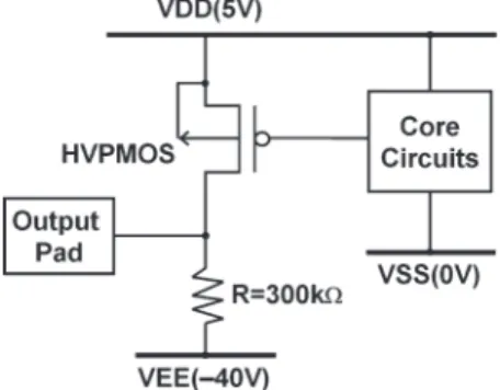
Fig. 1. Original output cell of the automotive VFD driver IC realized with the HVPMOS and pull-down resistor.
than that of the low-voltage MOSFET in CMOS technologies [1]–[7]. Hence, ESD reliability has been an important issue for HV IC products fabricated in CMOS technology.
In some specific applications, such as the driver IC for vacuum fluorescent display (VFD) [8] in automotive instrumen-tation [9], only HV p-channel MOS (HVPMOS) is provided in a given CMOS process, which is developed by adding a few additional masks and process steps into the low-cost low-voltage CMOS process. To reduce the fabrication cost, no HV n-channel MOS (HVNMOS) is used in such specific VFD driver IC. For safety concerns in automotive electronics, the ESD robustness was often requested to be much higher than that of consumer electronics products. Thus, an additional protection device is necessary in the HV I/O pin to sustain a high-enough ESD robustness of the VFD driver IC for safe automotive applications.
In this paper, a new ESD protection structure with the em-bedded HV p-type SCR (HVPSCR) into the HVPMOS device is proposed [10]. Only an additional n+ diffusion is added into the HVPMOS to form the HVPSCR for ESD protection. The HVPSCR device structure can greatly improve the human body model (HBM) ESD robustness of the VFD driver IC up to 8 kV in the specific 0.5-µm HV CMOS process for automotive electronics applications without suffering the latchup issue.
II. ORIGINALDESIGN FORVFD I/O
The HV output cell of the automotive VFD driver IC that was fabricated in a 0.5-µm HV CMOS process is shown in Fig. 1. In this VFD driver IC, the output pull-up function is realized by the HVPMOS, which is connected between the output pad and the
Fig. 2. Device structure of HVPMOS in the specific CMOS process. An HV p-well is used to surround the drain of HVPMOS to meet the HV application.
Fig. 3. DC I–V curve of HVPMOS in the low-current region, which has a breakdown voltage of 65 V.
VDD of 5 V, whereas the pull-down function is realized by an on-chip resistor of 300 kΩ for VFD. The resistor is connected from the output pad to the VEE of−40 V for VFD applications. Here, the internal core circuits are connected to the low-voltage power supply with the VDD of 5 V and VSS of 0 V.
A. Device Structure andI–V Characteristic of the HVPMOS The device structure of the HVPMOS is drawn in Fig. 2. The HV region is surrounded by an HV p-well of lightly doped concentration with a specified clearance from the HV p-well edge to the drain (p+ diffusion) of the HVPMOS, where the clearance is indicated as C in Fig. 2. Such HV p-well with lightly doped concentration will provide the drain of the HVPMOS with high-enough breakdown voltage for VFD application. The breakdown voltage of the HVPMOS is specified to be higher than 45 V for this VFD application.
While measuring the I–V characteristic of the HVPMOS in the VFD driver I/O cell, the gate of the HVPMOS is connected to the core circuits. The dc I–V curve of the HVPMOS in the low-current region measured by curve tracer 370 is shown in Fig. 3, where the breakdown voltage of this HVPMOS is ∼65 V. When the applied voltage is slightly larger than the breakdown voltage, the current will increase sharply. While the HVPMOS is switching fromOFF-state toON-state, the dc I–V curve behavior is shown in the curve of Fig. 3 and marked with “on.” However, while the HVPMOS is switching from
ON-state to OFF-state, the dc I–V curve behavior is shown
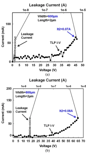
Fig. 4. TLP-measured I–V curves of HVPMOS (a) with a width of 600 µm and a length of 2 µm, and (b) with a width of 800 µm and a length of 2 µm.
in the curve of Fig. 3 and marked with “off.” There is no obvious snapback characteristic found in the dc I–V curve of HVPMOS. The transmission-line-pulsing-measured I–V curve of the HVPMOS with a width of 600 µm and a length of 2 µm is shown in Fig. 4(a). The trigger voltage (Vt1) of the TLP-measured I–V curve of HVPMOS is ∼35 V. Due to the inefficient parasitic p-n-p bipolar action in the HVPMOS, no obvious snapback characteristic is found. Therefore, the secondary breakdown current (It2) is only 0.07 A, which is quite low for ESD protection. Moreover, the TLP-measured I–V curve of the HVPMOS with a larger device size (with a width of 800 µm and a length of 2 µm) is shown in Fig. 4(b); the It2 is still only 0.08 A. Here, the difference on the trigger voltage of the HVPMOS measured by dc and TLP is caused by transient-coupling effect. The TLP is designed with a rise time of 10 ns to simulate the HBM ESD event. The fast TLP dV /dt transient voltage at the drain could be coupled into the device through the parasitic capacitance in the drain/bulk junction to lower the trigger voltage.
Fig. 5. Measured I–V curves of the HVPMOS (with a width of 600 µm and a length of 2 µm) in the VFD driver I/O cell before and after 1-kV ND-mode HBM ESD stress.
B. ESD Robustness and Failure Analysis (FA) of the HVPMOS in the VFD Driver IC
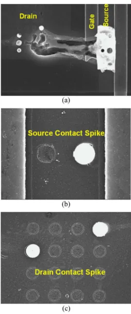
The HBM ESD levels and TLP-measured It2 of the HVPMOS in the VFD driver I/O cell with different device widths (but keeping the same length) are listed in Table I. With device widths of 500, 600, and 800 µm, the It2 of the HVPMOS are 0.04, 0.07, and 0.08 A, respectively. For such a lower It2, the HBM ESD levels of the HVPMOS are all about∼500 V under the ND-mode ESD stress. Here, the failure criterion is defined at a leakage current that is greater than 1 µA under a 45-V bias on the devices. The measured I–V curves of the HVPMOS (with a width of 600 µm and a length of 2 µm) in the VFD driver I/O cell before and after 1-kV ND-mode HBM ESD stress are shown in Fig. 5, where the voltage that is applied at VDD, with the output pad grounded, is swept from 0 to 45 V. Before ESD stress, the HVPMOS is turned off, so that there is no leakage current between the VDD and output pad. However, after ESD stress, the HVPMOS is burned out to cause a short circuit in the I–V curve. The FA picture of this output cell on the HVPMOS (with a width of 600 µm and a length of 2 µm) after 1-kV ND-mode HBM ESD stress is shown in Fig. 6(a), where serious contact spiking from the drain to source of the HVPMOS is found. Moreover, the enlarged pictures of contact spiking in the source and drain regions are shown in Fig. 6(b) and (c), respectively, where the lightened contacts are damaged by HBM ESD stress. Due to the too low TLP-measured It2 and ESD levels, the HVPMOS is not suitable as the ESD protection device for the output cell of the VFD driver IC.
Fig. 6. Scanning electron microscope failure pictures of (a) the output HVPMOS with a device width of 600 µm and a length of 2 µm, (b) the contact spiking in the source region of HVPMOS, and (c) the contact spiking in the drain region of HVPMOS, in the VFD driver IC after 1-kV ND-mode HBM ESD stress.
III. NEWESD DESIGN FORVFD I/O
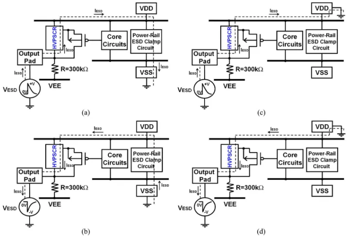
A new ESD protection structure with the HVPSCR embed-ded into the output HVPMOS is proposed to greatly improve the ESD robustness of the automotive VFD driver IC. The output cell with the embedded HVPSCR for automotive VFD drive IC is shown in Fig. 7. With the addition of power-rail ESD clamp circuit [11], the positive-to-VSS (PS-mode), negative-to-VSS (NS-mode), positive-to-VDD (PD-mode), and ND-mode ESD stresses [12], [13] on the output pin can be discharged through the HVPSCR to the VSS or VDD with the cooperation of the power-rail ESD clamp circuit.
A. Device Structure and Turn-On Mechanism of the HVPSCR The device structure of the HVPSCR embedded into the output HVPMOS is drawn in Fig. 8, where an additional
Fig. 7. New proposed ESD protection design with the HVPSCR embedded into the output HVPMOS to improve the ESD robustness of the output cell of the automotive VFD driver IC.
Fig. 8. Device structure of the HVPSCR embedded into the output HVPMOS.
n+ diffusion is inserted into the drain region in the HV p-well of the HVPMOS. The SCR path in the HVPSCR is from VDD to the output pad, which is composed of p+ diffusion (source of HVPMOS), n-well, HV p-well (drain of HVPMOS), and n+ diffusion in the HV p-well. Here, only an additional n+ diffusion is added into the HVPMOS to form the HVPSCR for ESD protection. So, only a little increase of silicon area is used to realize this HVPSCR. The final die size of the VFD driver IC with the proposed HVPSCR for ESD protection is almost kept the same.
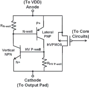
The equivalent circuit of the HVPMOS with the embedded HVPSCR device is shown in Fig. 9, where the anode of the HVPSCR is connected to VDD and the cathode of HVPSCR is connected to the output pad. The HVPSCR device is composed of a lateral p-n-p bipolar transistor and a vertical n-p-n bipolar transistor to form a two-terminal/four-layer p-n-p-n (p+/n-well/HV p-well/n+) structure. The trigger voltage of the HVPSCR device is the same as that of the HVPMOS, which is determined by the drain avalanche breakdown voltage of the n-well/HV p-well junction, such that, while the overstress voltage reaches the breakdown voltage of the n-well/HV p-well junction, the embedded HVPSCR will be triggered on to discharge the ESD current. The turn-on mechanism of the HVPSCR is somewhat similar to that of p-channel MOS (PMOS)-triggered SCR [14], [15], where the PMOS is first turned on by the ESD transient pulse and then the SCR can be triggered on when the current reaches the trigger current of the SCR.
During PD-mode ESD stress, positive ESD voltage is applied to the output pad, and VDD is relatively grounded. The parasitic
Fig. 9. Equivalent circuit of the HVPMOS with the embedded HVPSCR.
diode (n-well/HV p-well junction) of the HVPMOS will be forward biased to clamp the ESD voltage. During the ND-mode ESD stress, the negative ESD voltage is applied to the output pad, and VDD is relatively grounded. When the magnitude of the applied voltage is greater than the drain breakdown voltage of HVPMOS, the hole and electron current will be generated through the avalanche breakdown mechanism. The electron current will flow through the n-well to the n+ diffusion connected to the anode of HVPSCR, which will lower the voltage level of the n-well. As long as the voltage drop across n-well resistor Rn-well is greater than the turn-on voltage of the lateral p-n-p transistor, the lateral p-n-p transistor will be triggered on to keep HVPMOS into its breakdown region. While the lateral p-n-p transistor is turned on, the hole current will be injected through the HV p-well into the p+ diffusion (connected to cathode of HVPSCR) to increase the voltage level of the HV p-well. As the injected hole current is larger than some critical value, the voltage drop across the HV p-well resistor RHV p-well will be greater than the turn-on voltage of the vertical n-p-n transistor. The vertical n-p-n transistor will be turned on to inject the electron current through the n-well into the n+ diffusion to further bias the lateral p-n-p transistor. Such positive feedback regeneration physical mechanism [16], [17] will initiate the latching action in the HVPSCR. Finally, the HVPSCR will be successfully triggered into its latching state with the positive-feedback regenerative mechanism [16], [17]. Once the HVPSCR is triggered on, the required holding current to keep the n-p-n and p-n-p transistors on can be gener-ated through the positive-feedback regenerative mechanism of latchup without involving the avalanche breakdown mechanism again. So, the HVPSCR will have a lower holding voltage than HVPMOS. Therefore, the ND-mode ESD current can be effectively discharged by the HVPSCR to protect the VFD driver IC.
The latchup issue [18], [19] should be considered when the HVPSCR is used for ESD protection. When ICs are in normal circuit operating conditions, the HVPSCR device could be accidentally triggered on by noise pulse [20]. However, for VFD application, during normal circuit operating conditions,
Fig. 10. Circuit schematic of the power-rail ESD clamp circuit, which is composed by a resistor, capacitor, inverter, and NMOS.
the current from VDD through the HVPSCR to VEE will be limited to some a smaller value of∼0.15 mA by the large pull-down resistor R of 300 kΩ. Such a limited current is much lower than the holding current (∼35 mA, from the measured result in silicon) of the HVPSCR, which can avoid the latchup issue between the power lines during normal circuit operating conditions. On the other hand, if the HVPMOS is triggered on by the transient noise pulse, the unwanted transient noise current will flow through the HVPMOS and be absorbed by the VDD power supply. Therefore, the latchup problem will not occur in such VFD driver IC with the HVPSCR embedded into the HVPMOS.
B. ESD Protection Design for VFD I/O With Both HVPSCR and Power-Rail ESD Clamp Circuit
To sustain high ESD robustness for VFD I/O, the power-rail ESD clamp circuit between VDD and VSS is added to support the ESD discharge path between the output pad and VSS. The power-rail ESD clamp circuit composed of resistor, capacitor, inverter, and n-channel MOS (NMOS) is shown in Fig. 10. Here, the RC value is designed with a time constant of about∼1 µs to distinguish the VDD power-on event (with a rise time in milliseconds) or ESD stress events (with a rise time in nanoseconds) [11]. During the normal VDD power-on transitipower-on (from low to high), the input of the inverter can follow up in time with the power-on VDD voltage to keep the output of the inverter at zero. Hence, the NMOS device is kept off and does not interfere with the functions of the internal circuits. When a positive ESD voltage is applied to VDD, with VSS relatively grounded, the RC delay will keep the input of the inverter at a low-voltage level within a relative long time. Therefore, the output of the inverter will be pulled high by the ESD energy to trigger on the NMOS device. While the NMOS device is turned on, the ESD current is discharged from VDD to VSS through the NMOS device. When a negative ESD voltage is applied to VDD, with VSS relatively grounded, the negative ESD current can be discharged through the forward-biased drain-to-bulk parasitic diode in the NMOS.
The ESD current paths of the new proposed ESD protec-tion for VFD I/O in four ESD-stress modes are shown in Fig. 11(a)–(d). Under the PS-mode ESD-stress condition, the ESD current will flow from the output pad through the parasitic diode of HVPMOS to VDD and then through the power-rail
new proposed ESD protection design can provide a higher ESD level for such VFD driver ICs.
For VFD application, because of the large resistor R of 300 kΩ between the output pad and VEE, the ESD current from the output pad to VEE will be limited by resistor R. Hence, both positive and negative ESD stresses on the output pad, with VEE relatively grounded, can sustain high ESD robustness.
IV. EXPERIMENTALRESULT
A. I–V Characteristic of the HVPSCR
The dc I–V curve of the HVPSCR measured by curve tracer 370 under room temperature of 25◦C is shown in Fig. 12(a), where the dc trigger voltage of HVPSCR is∼65 V, which is the same as that of HVPMOS. Before the SCR path is triggered on, the dc I–V curve behavior of HVPSCR is the same as that of HVPMOS. When the current is larger than∼5 mA, the embedded HVPSCR is triggered on into its holding state with a dc holding voltage of∼5 V. While the HVPSCR is switching fromOFF-state toON-state, the dc I–V curve behavior is shown in the curve of Fig. 12(a) and marked with “on.” However, while the HVPSCR is switching fromON-state toOFF-state, the dc I–V curve behavior is shown in the curve of Fig. 12(a) and marked with “off,” where the holding current is about∼35 mA. Because the holding voltage of the HVPSCR is smaller than the operation voltage (45 V), the HVPSCR could be triggered on to suffer latchup failure in the VFD driver IC by the transient noise pulse. However, the maximum dc operation current across the pull-down resistor R between the output pad and the VEE power pad is 0.15 mA. This dc current is obtained from the maximum voltage drop, which is 45 V (between VDD and VEE) divided by 300 kΩ when the pull-up HVPMOS is turned on. The current of 0.15 mA is less than the dc holding current (∼35 mA) of the HVPSCR, which can avoid the latchup issue between the power lines during normal operating conditions. Moreover, the dc I–V curve of the HVPSCR measured by curve tracer 370 under a temperature of 125 ◦C is shown in Fig. 12(b), where the holding voltage (current) is decreased from∼5 V (∼35 mA) to ∼3 V (∼20 mA), as the temperature is increased from 25◦C to 125◦C. Although the latchup problem is very sensitive to high temperature, the maximum current flowing across the resistor is still kept at 0.15 mA for the high temperature due to the large resistor R. The HVPSCR cannot stay in its turn-on state if the supplied current is smaller than its holding current. Hence, even for high ambient temperatures such as 125 ◦C, the HVPSCR is still kept at the OFF-state to avoid the latchup problem. Hence, under normal circuit operating conditions, the HVPSCR can be free from the latchup problem between the power lines in the VFD driver IC, despite
Fig. 11. ESD current paths on the VFD driver IC with HVPSCR and power-rail ESD clamp circuit under (a) PS-mode, (b) NS-mode, (c) PD-mode, and (d) ND-mode ESD-stress conditions.
of a potentially low dc holding voltage below the operation voltage.
The TLP-measured I–V curve of the HVPSCR with a width of 600 µm and a length of 2 µm is shown in Fig. 13. The trigger voltage of the HVPSCR in the TLP-measured I–V curve is about∼53 V, and the trigger current is about 0.27 A. Moreover, in the inset figure, a high trigger current of almost 0.27 A can be obviously found, where the latchup immunity can be achieved over 200 mA by preventing unwanted triggering during normal circuit operation. Here, before the HVPSCR is triggered on, the HVPMOS will handle the low TLP current. As the TLP current is higher than 270 mA, the HVPSCR will be fully turned on. With the excellent clamping behavior of the HVPSCR, a very low holding voltage of the HVPSCR can be obtained around 5 V. According to the power dissipation of P = I× V , where I indicates the ESD discharge current and V indicates the holding voltage of the device, the device with a lower holding voltage during ESD stress can sustain a higher ESD level. The TLP-measured It2 of HVPSCR is greater than 6 A, which is much higher than that (0.07 A) of HVPMOS. So, the HVPSCR can indeed sustain a much higher ESD level for the output cell of this VFD driver IC.
From the previous work [21], a similar solution was proposed to improve the ESD robustness in a smart-power IC. An ESD robust output switch, which is called SCR–laterally diffused MOS (SCR–LDMOS), was modified from the standard lateral LDMOS without any additional processing, where the device
structure of SCR–LDMOS is redrawn in Fig. 14 [21]. The characteristics of the SCR–LDMOS are kept the same as those of the LDMOS during normal circuit operating conditions, and the SCR (p+/n-well/p-well/n+) will be turned on to a low holding voltage to discharge the ESD current during ESD stress. However, no n-type HV device (such as HVNMOS) was provided in this paper with the cost-efficient CMOS process for the VFD driver IC. So, such an SCR–LDMOS cannot be applied in our VFD driver IC to improve ESD robustness. Moreover, even with the use of SCR–LDMOS in smart-power technology, the latchup problem still has to be watched during normal circuit operating conditions. In our work, the use of the HVPSCR did not cause a latchup problem between the power lines in such VFD driver IC due to the large resistor R between the output pad and VEE.
B. ESD Robustness of the VFD Driver IC
TLP-measured It2, and the HBM and machine-model (MM) ESD levels of the HVPSCR under different device widths (but the same length) are shown in Table II. The It2 of the HVPSCR with device widths of 500, 600, and 800 µm are all over 6 A, whereas the HBM ESD levels can pass over 8 kV under ND-mode ESD stress. Moreover, with device widths of 500, 600, and 800 µm, the MM ESD levels of the HVPSCR are 1100, 1300, and 1900 V, respectively. With both the new proposed HVPSCR embedded into the HVPMOS and the
Fig. 12. DC I–V curves of the HVPSCR (a) with a dc trigger voltage of 65 V and a holding voltage (current) of∼5 V (∼35 mA) under a temperature of 25◦C, and (b) with a dc trigger voltage of 65 V and a holding voltage (current) of∼3 V (∼20 mA) under a temperature of 125◦C.
Fig. 13. TLP-measured I–V curve of HVPSCR with a width of 600 µm and a length of 2 µm. A high trigger current of∼270 mA can be seen in the inset drawn in the low-current region, so the HVPSCR can be fully triggered on when the current reaches above 270 mA.
power-rail ESD clamp circuit, the HBM ESD robustness of the output cell in the automotive VFD driver IC has been successfully improved from 500 V up to 8 kV within almost the same die size.
The partial layout view of this VFD driver IC with HVPSCR in the I/O cell is shown in Fig. 15, which can fully meet the
Fig. 14. Device structure of SCR–LDMOS [21]. TABLE II
TLP_It2, HBM,ANDMM ESD LEVELSUNDERND-MODE
ESD STRESSES OF THEHVPSCR
Fig. 15. Partial layout view of the VFD driver IC with the HVPSCR in the I/O cell, which can sustain HBM ESD stress of up to 8 kV.
ESD specification of automotive applications. Moreover, the automotive driver IC has also successfully passed the 200-mA quasi-static latchup test of EIA/JEDEC standard [22]. Such an ESD-enhanced driver IC has been in mass production for VFD applications in a car.
V. CONCLUSION
The HVPMOS is not suitable for ESD protection in a VFD driver IC for automotive electronics applications due to its poor ESD level. To greatly improve ESD robustness, a new ESD pro-tection structure of the HVPSCR embedded into the HVPMOS is proposed by only adding an additional n+ diffusion into the drain region of HVPMOS. With almost the same layout area, the It2 of the output cell has been improved over 6 A, and the HBM ESD level of such VFD driver IC with HVPSCR can sustain up to 8 kV. With device widths of 500, 600, and 800 µm, the MM ESD levels of the HVPSCR are 1100, 1300, and
1900 V, respectively. Moreover, the automotive driver IC can also pass the 200-mA quasi-static latchup test.
ACKNOWLEDGMENT
The authors would like to thank M. Yang, C.-C. Chen, M.-C. Chan, W.-T. Shieh, and K.-L. Yen of ELAN Micro-electronics Corporation, Hsinchu, Taiwan, R.O.C., for their support on this work; and the Editor and his reviewers for their valuable suggestions to improve this paper. The second author was supported by the MediaTek Fellowship, Hsinchu, Taiwan.
REFERENCES
[1] M. P. J. Mergens, W. Wilkening, S. Mettler, H. Wolf, A. Stricker, and W. Fichtner, “Analysis of lateral DMOS power devices under ESD stress conditions,” IEEE Trans. Electron Devices, vol. 47, no. 11, pp. 2128– 2137, Nov. 2000.
[2] C. Duvvury, F. Carvajal, C. Jones, and D. Briggs, “Lateral DMOS design for ESD robustness,” in IEDM Tech. Dig., 1997, pp. 375–378.
[3] C. Duvvury, J. Rodriguez, C. Jones, and M. Smayling, “Device integration for ESD robustness of high voltage power MOSFETs,” in IEDM Tech.
Dig., 1994, pp. 407–410.
[4] J.-H. Lee, J.-R. Shih, C.-S. Tang, K.-C. Liu, Y.-H. Wu, R.-Y. Shiue, T.-C. Ong, Y.-K. Peng, and J.-T. Yue, “Novel ESD protection structure with embedded SCR LDMOS for smart power technology,” in Proc. IEEE
Int. Reliab. Phys. Symp., 2002, pp. 156–161.
[5] V. De Heyn, G. Groeseneken, B. Keppens, M. Natarajan, L. Vacaresse, and G. Gallopyn, “Design and analysis of new protection structures for smart power technology with controlled trigger and holding voltage,” in
Proc. IEEE Int. Reliab. Phys. Symp., 2001, pp. 253–258.
[6] G. Bertrand, C. Delage, M. Bafleur, N. Nolhier, J. Dorkel, Q. Nguyen, N. Mauran, D. Tremouilles, and P. Perdu, “Analysis and compact mod-eling of a vertical grounded-base n-p-n bipolar transistor used as ESD protection in a smart power technology,” IEEE J. Solid-State Circuits, vol. 36, no. 9, pp. 1373–1381, Sep. 2001.
[7] M.-D. Ker and K.-H. Lin, “The impact of low-holding-voltage issue in high-voltage CMOS technology and the design of latchup-free power-rail ESD clamp circuit for LCD driver ICs,” IEEE J. Solid-State Circuits, vol. 40, no. 8, pp. 1751–1759, Aug. 2005.
[8] N. Boswell, “Vacuum fluorescent display developments,” in Proc. IEE
Colloq. Graph. Display Devices, 1989, pp. 3/1–3/2.
[9] A. Slack, “Prospective developments in automotive instrumentation,” in
Proc. IEEE Int. Electron. Manuf. Technol. Symp., 1998, pp. 10–15.
[10] M.-D. Ker, W.-J. Chang, M. Yang, C.-C. Chen, M.-C. Chan, W.-T. Shieh, and K.-L. Yen, “ESD protection structure with embedded high-voltage p-type SCR for automotive vacuum-fluorescent-display (VFD) applica-tions,” in Proc. IEEE Int. Symp. IPFA, 2005, pp. 67–70.
[11] M.-D. Ker, “Whole-chip ESD protection design with efficient
VDD-to-VSS ESD clamp circuits for submicron CMOS VLSI,” IEEE
Trans. Electron Devices, vol. 46, no. 1, pp. 173–183, Jan. 1999.
[12] ESD Association Standard Test Method ESD STM5.1-1998, for
Electrostatic Discharge Sensitivity Testing—Human Body Model (HBM)—Component Level, 1998.
[13] ESD Association Standard Test Method ESD STM5.2-1999, for
Electro-static Discharge Sensitivity Testing—Machine Model—Component Level,
1999.
[14] B. Keppens, M. P. J. Mergens, C. S. Trinh, C. C. Russ, B. V. Camp, and K. G. Verhaege, “ESD protection solutions for high voltage technologies,” in Proc. EOS/ESD Symp., 2004, pp. 289–298.
[15] M.-D. Ker, C.-Y. Wu, and H.-H. Chang, “Complementary-LVTSCR ESD protection circuit for submicron CMOS VLSI/ULSI,” IEEE Trans.
Electron Devices, vol. 43, no. 4, pp. 588–598, Apr. 1996.
[16] M.-D. Ker and C.-Y. Wu, “Modeling the positive feedback regenerative process of CMOS latchup by a positive transient pole method—Part I: Theoretical derivation,” IEEE Trans. Electron Devices, vol. 42, no. 6, pp. 1141–1148, Jun. 1995.
[17] M.-D. Ker and C.-Y. Wu, “Modeling the positive feedback regenerative process of CMOS latchup by a positive transient pole method—Part II: Quantitative evaluation,” IEEE Trans. Electron Devices, vol. 42, no. 6, pp. 1149–1155, Jun. 1995.
[18] M. J. Hargrove, S. Voldman, R. Gauthier, J. Brown, K. Duncan, and W. Craig, “Latchup in CMOS technology,” in Proc. IEEE Int. Reliab.
Phys. Symp., 1998, pp. 269–278.
[19] M.-D. Ker, “Lateral SCR devices with low-voltage high-current trig-gering characteristics for output ESD protection in submicron CMOS technology,” IEEE Trans. Electron Devices, vol. 45, no. 4, pp. 849–860, Apr. 1998.
[20] M.-D. Ker and H.-H. Chang, “How to safely apply the LVTSCR for CMOS whole-chip ESD protection without being accidentally triggered on,” J. Electrostat., vol. 47, no. 4, pp. 215–248, Oct. 1999.
[21] S. Pendharkar, R. Teggatz, J. Devore, J. Carpenter, T. Efland, and C.-Y. Tsai, “SCR-LDMOS: A novel LDMOS device with ESD robust-ness,” in Proc. Power Semicond. Devices ICs Symp., 2000, pp. 341–344. [22] IC Latch-Up Test. Electron. Industries Assoc., EIA/JEDEC Stand. 78,
1997.
Ming-Dou Ker (S’92–M’93–SM’97) received the
B.S., M.S., and Ph.D. degrees from National Chiao-Tung University, Hsinchu, Taiwan, R.O.C., in 1986, 1988, and 1993, respectively.
In 1994, he joined the VLSI Design Department, Computer and Communication Research Laborato-ries (CCL), Industrial Technology Research Institute (ITRI), Taiwan, as a Circuit Design Engineer. In 1998, he was the Department Manager of the VLSI Design Division, CCL/ITRI. He is currently a Full Professor with the Nanoelectronics and Gigascale Systems Laboratory, Department of Electronics Engineering, National Chiao-Tung University. He has been invited to teach or to consult reliability and quality design for integrated circuits by hundreds of design houses and semi-conductor companies in the Science-Based Industrial Park, Hsinchu, Taiwan; in the Silicon Valley, San Jose, CA; in Singapore; in Malaysia, and in Mainland China. In the field of reliability and quality design for CMOS integrated circuits, he has published more than 300 technical papers in international journals and conference proceedings. He has proposed many inventions to improve the reliability and quality of integrated circuits, which have been granted with 125 U.S. patents and 135 R.O.C. (Taiwan) patents. His current research interests include reliability and quality design for nanoelectronics and gigascale systems, high-speed and mixed-voltage I/O interface circuits, and on-glass circuits for system-on-panel applications in TFT LCD display.
Dr. Ker has served as member of the Technical Program Committee and Session Chair of numerous international conferences. He was selected as a Distinguished Lecturer in IEEE Circuits and Systems Society for 2006–2007. He has also served as Associate Editor for the IEEE TRANSACTIONS ONVERY
LARGESCALEINTEGRATIONSYSTEMS. He was elected as the President of Taiwan ESD Association in 2001. He was the recipient of many research awards from ITRI, National Science Council, National Chiao-Tung University, and the Dragon Thesis Award from Acer Foundation. In 2003, he was selected as one of the Ten Outstanding Young Persons in Taiwan by Junior Chamber International. In 2005, one of his patents on ESD protection design was awarded with the National Invention Award in Taiwan.
Wei-Jen Chang (S’02) was born in Taiwan, R.O.C.,
in 1979. He received the B.S. degree from National Chiao-Tung University, Hsinchu, Taiwan, in 2002. He is currently working toward the Ph.D. degree at the Nanoelectronics and Gigascale Systems Labo-ratory, Department of Electronics Engineering, Na-tional Chiao-Tung University.
His current research interests include ESD protec-tion design for mixed-voltage I/O circuits and high-voltage applications.
Mr. Chang was the recipient of the MediaTek Fellowship Award.