Performance Improvement of CoTiO
3High-k Dielectrics with
Nitrogen Incorporation
Jian Hao Chen,aTzung Bin Huang,bXiaohua Wu,cDolf Landheer,c,
*
Tan Fu Lei,aand Tien Sheng Chaob,za
Institute of Electronics and Department of Electrical Engineering, and bDepartment of Electrophysics, National Chiao Tung University, Hsinchu 30010, Taiwan
c
Institute for Microstructural Sciences, National Research Council of Canada, Ottawa, Ontario, K1A 0R6 Canada
In this paper, three approaches to incorporating nitrogen in CoTiO3high-k dielectric films, ion implantation of N2+, ion
implanta-tion of N+, and N
2O plasma treatment have been investigated for the new CoTiO3high-k dielectrics. All three methods reduced the
leakage currents and improved the breakdown characteristics but the N2O-plasma treatment produced the best-behaved C-V
curves, when compared to the untreated control samples.
© 2006 The Electrochemical Society. 关DOI: 10.1149/1.2388733兴 All rights reserved.
Manuscript submitted June 30, 2006; revised manuscript received September 29, 2006. Available electronically December 4, 2006.
The thickness of the conventional silicon dioxide 共SiO2兲 gate
dielectrics has been scaled down to around 1.5 nm to meet the high drive requirements of high-performance共CMOS兲.1The most serious problem we face today for this ultrathin gate dielectric is the huge gate leakage due to the direct tunneling of carriers from the channel of metal oxide semiconductor field-effect transistors共MOSFET兲s,2 which reduces the transconductance of devices, and increases the standby power. This is not adequate for low-power applications in portable equipment. For a long time, high dielectric constant 共high-k兲 gate materials such as Si3N4,3,4 Al2O3,5-7 HfO2,8-10 and
ZrO211-13have been proposed to replace the conventional ultrathin
SiO2to solve this problem. For the same equivalent-oxide-thickness 共EOT兲, the thickness of high-k gate dielectrics can be increased many times. Hence, the direct tunneling current can be significantly reduced. The choice of high-k material is based on the following requirements:
1. The k-value should be in the range 20-50, as high as possible but low enough to avoid the fringing-induced barrier lowering effect in sub-100 nm nMOSFETs.14
2. The bandgap energy should be larger than 4.5 eV and barrier height larger than 1 eV to avoid increased leakage current at el-evated temperature.15,16
3. The interface state density should be less than 1011cm−2eV−1 to maintain a well-behaved subthreshold characteristic.
4. Low trap densities are required in the film to avoid Frankel-Poole tunneling.
5. The dielectric should have good thermal stability during the high-temperature processing.
6. It should have high breakdown voltage, low-leakage, and low hysteresis. In our previous paper, a new high-k dielectric CoTiO3
has been proposed for application in MOSFETs and dynamic ran-dom access memories共DRAMs兲.17The dielectric constant for this CoTiO3 with the bottom oxide layer can be as high as 50, which
makes this high-k dielectric become very promising after the current medium k value 共15–25兲 materials, such as HfO2 and ZrO2, have reached their useful limit. However, some issues still remain when high-k materials are used. The most important issues are:
1. The interfacial layer of SiO2or silicate remaining after
depo-sition of high-k materials.
2. The high fixed charge in the bulk of high-k dielectrics which results in flabband voltage共VFB兲 shifts.
3. The degradation of mobility.
4. A low crystallization temperature.
5. Boron penetration for pMOSFETs. According to recent reports,18-32 optimized treatments which incorporate nitrogen have resulted in a significant improvement in the high-k dielectric prop-erties. Nitridation of the silicon surface can reduce the growth of an interfacial layer. Plasma nitridation after deposition of the high-k dielectric can recover the degradation of mobility. The advantages of nitrogen incorporation are the increase of the k-value, the increase of the temperature of crystallization, the reduction of the leakage, reasonable VFB, and reduced boron penetration.18-31 Because we
have investigated the material and electrical properties in Ref. 33 and 34, in this paper, nitrogen incorporation using N2+/N+ ion
im-plantation or N2O plasma treatment to improve this CoTiO3films investigated. We found that the nitrogen incorporation by either ion implantation or plasma treatment can be used to significantly im-prove the electrical performance of CoTiO3high-k dielectrics.
Experimental
Capacitors were fabricated on n-type 150 mm Si具100典 wafers with a resistivity of 2-7⍀ cm. After the growth of a 550 nm thick field oxide, the active region of capacitors were defined and etched by buffered oxide etch共BOE, NH4F: HF = 6:1兲. Wafers underwent
a RCA standard cleaning process and were put into the low-pressure chemical vapor deposition共LPCVD兲 tube in a pure NH3ambient to grow an ultrathin nitride⬃1.0 nm thick on the Si surface. The thick-ness of the nitride was measured by ellipsometery. The purpose of this NH3-grown ultrathin nitride film is to prevent the reaction of the
following sputtered Ti and then Co共Co/Ti兲 metal films, and also to retard the oxidation of silicon during the oxidation of Co/Ti layer. The Ti共5 nm兲 and Co 共5 nm兲 films were deposited by sputtering at a power of 500 W, and a sputtering rate was of 0.9 nm/s. Then wafers underwent the N2+ or N+ ion implantation. To avoid the
ni-trogen penetration through the metal films and to reduce damage of the metal films, a low ion energy of 10 keV was used with nitrogen doses of 2⫻ 1014and 2⫻ 1015atom/cm2. Wafers were then oxi-dized in the furnace using flows of 5000 sccm each of O2and N2. Splits were done for oxidation temperatures of 800, 850, and 900°C, and the oxidation time was 10 min. Some wafers without nitrogen implantation underwent N2O plasma treatment in a plasma
en-hanced chemical vapor deposition共PECVD兲 system. The flow rate of N2O was 60 sccm, the temperature was 350°C, the power was set at 10, 15, or 20 W, and the processing time was 5 min. The purpose of this N2O plasma treatment is to passivate the oxygen vacancies in
the bulk film, and also to incorporate nitrogen in the dielectrics. The top electrode for electrical measurements was a 500 nm Al film which was deposited by physical vapor deposition共PVD兲. The ca-pacitance voltage 共C-V兲 curves of the capacitors were measured
*Electrochemical Society Active Member. z
with a HP 4284 impedance meter at 100 kHz. The areas of the capacitors were 2.5⫻ 10−5cm2 共50 ⫻ 50 m兲 and 1 ⫻ 10−4cm2
共100 ⫻ 100 m兲. The current-voltage 共I-V兲 curves were measured using a HP 4156 parameter analyser. The properties of high-k dielec-trics with and without nitrogen incorporation were analyzed by transmission electron microscopy共TEM兲, secondary-ion mass spec-trometry共SIMS兲, and X-ray diffraction 共XRD兲.
Results and Discussion
The thickness of all CoTiO3 samples was first measured by TEM. Figure 1a and b show one set of the TEM pictures for samples of CoTiO3oxidized at 800°C for 10 min without and with nitrogen ion implantation, respectively. The physical thickness of both samples was in the range 24–25 nm. It was observed that the oxi-dation of the Ti/Co films increases the thickness of the interfacial layer. This indicates that the ultrathin nitride film was not thick enough to retard the diffusion of oxygen. Compared with the sample without nitrogen implantation, smaller grains and a less diffuse boundary profile between high-k and interfacial layers were found for the N2+-implanted sample. C-V curves at a high frequency of 100 kHz are shown in Fig. 2. The C-V curves for samples oxidized at 800°C for 10 min without nitrogen implantation were not ob-tained due to a large leakage current during measurement. This may be due to the nonfully oxidized Co/Ti in the bulk of dielectrics at
lower temperature for a short oxidation time of 10 min. It was found that the accumulation of CoxCox decreases as the oxidation
tempera-ture was increased due to abundant oxygen incorporation during the oxidation step. The extract equivalent-oxide-thickness共EOT兲, inter-facial silicate thickness, high-k dielectric thickness, total thickness, effective k-value and flatband voltage are complied and shown in Table I. The existing interfacial layer degrades the effective k-value. However, in Ref. 17 we have estimated the intrinsic bulk dielectrics constant for CoTiO3under the same processes. The intrinsic bulk
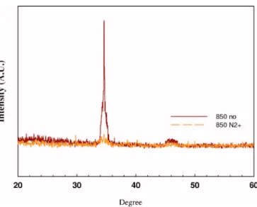
dielectric constant was estimated as high as 50, excluding the inter-facial layer. It was found that the EOT increases as the oxidation temperature increased. As a result, the effect k-value deduced from the result of C-V and TEM measurements decreases as the tempera-ture is increased. The flatband voltage shifts to a negative value for the sample oxidized at 900°C with nitrogen implantation. This may be due to nitrogen diffusion into the interfacial layer which creates positive charges in the film. Figure 3 shows the electrical properties for samples oxidized at 900°C for 10 min. Figure 3a shows that capacitors with nitrogen ion implantation exhibit a lower leakage current and high breakdown voltage. This phenomenon is the same for samples with 800° and 850°C oxidation. Figure 3b shows the Weibull distribution of gate leakage current at Vg= 1 V. Capacitors with nitrogen implantation have a tighter distribution and smaller leakage than those without. Figure 3c shows the Weibull distribution of breakdown voltage for two samples. Once again, the capacitors with nitrogen implantation have higher breakdown voltage than the ones without. The two samples were also subjected to constant volt-age共Vg= 2 V兲 stress and the results are shown in Fig. 4a and b. For the capacitors without nitrogen implantation, a significant increase of gate leakage was found when the stress time was increased to 100 s compared with the implanted samples. On the other hand, the samples with nitrogen implantation exhibited no significant in-creased gate leakage when compared to the capacitor without nitro-gen implantation. The X-ray diffraction spectrum is shown in Fig. 5 for a CoTiO3 film oxidized at 850°C with and without nitrogen
implantation. For the sample without nitrogen implantation, a clear peak intensity was found around 34° for CoTiO3共311兲 but the peak
is not so clear for the sample with nitrogen implantation. This im-plies that the nitrogen implantation of the Ti/Co films can retard the crystallization of CoTiO3.
To reduce the damage from the nitrogen ion implantation, two approaches were adopted. The first approach was to reduce the mass of implanted species by using N+instead of N2+. Figure 6a shows the result. The oxidation temperature was 850°C with a reduced oxida-tion time of 5 min. This can reduce the oxygen encroachment during the high temperature oxidation. The leakage current decreased as the nitrogen dose increased. The Weibull distributions of gate leakage current and breakdown voltage are shown in Fig. 6b and c, respec-tively. It can be seen that high nitrogen doses improve the electrical properties of the capacitors.
The second approach to avoid the damage from ion implantation was generally to use the N2 plasma treatments34-36 or post-deposition annealing共PDA兲 in nitrogen ambient, such as N2, NO,
N2O, or HH3.37,38In this work, we use N2O plasma treatment共at Figure 1. TEM pictures for samples of CoTiO3 oxidized at 800°C for
10 min共a兲 without and 共b兲 with nitrogen ion implantation.
Figure 2.共Color online兲 High-frequency C-V curves measured at 100 kHz for all samples oxidized at 800, 850, and 900°C with or without nitrogen implantation.
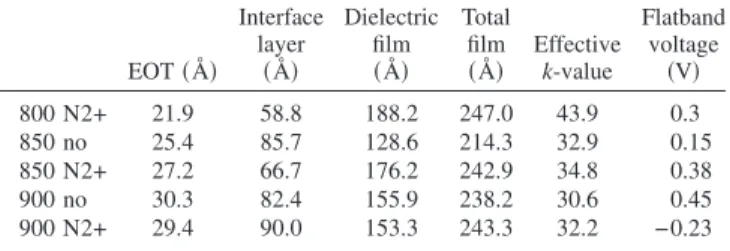
Table I. The resultant equivalent-oxide-thickness (EOT), inter-face layer, CoTiO3dielectric thickness, total thickness, effective k-value, and flatband voltage for all samples.
EOT共Å兲 Interface layer 共Å兲 Dielectric film 共Å兲 Total film 共Å兲 Effectivek-value Flatband voltage 共V兲 800 N2+ 21.9 58.8 188.2 247.0 43.9 0.3 850 no 25.4 85.7 128.6 214.3 32.9 0.15 850 N2+ 27.2 66.7 176.2 242.9 34.8 0.38 900 no 30.3 82.4 155.9 238.2 30.6 0.45 900 N2+ 29.4 90.0 153.3 243.3 32.2 −0.23 G19
powers of 10, 15, and 20 W兲 after the oxidation step. Some samples without nitrogen ion implantation underwent the N2O plasma
treat-ment before metal deposition. This treattreat-ment can passivate the oxy-gen vacancies共radical of oxygen in N2O plasma兲 in the dielectric
Figure 3.共Color online兲 I-V curves of samples oxidized at 900°C for 10 min with and without nitrogen implantation.共a兲 Gate voltage vs gate leakage current.共b兲 Weibull distribution of gate leakage current at Vg= 1 V.共c兲
Weibull distribution of breakdown voltage.
Figure 4.共Color online兲 The I-V curves for samples oxidized at 850°C for 10 min共a兲 without and 共b兲 with nitrogen implantation after constant voltage stress at Vg= 2 V for 100 s.
Figure 5. 共Color online兲 XRD spectrum for a CoTiO3 film oxidized at
bulk and also introduce nitrogen共radical of nitrogen in N2O plasma兲 in the bulk. Figure 7 shows the SIMS profile for samples with N2O plasma treatment共20 W兲. We found that nitrogens pile up at the high-k/Si interface using N2O plasma. This profile is different from
the report using N2plasma in which the nitrogen was diffused uni-formly into the bulk after annealing at 700°C.36However, this result is similar to the resultant nitrogen profile in ultrathin gate oxide共or oxy-nitride兲 formed by N2O oxidation or annealing.39Another
ad-vantage using N2O plasma instead of N2plasma is the oxygen
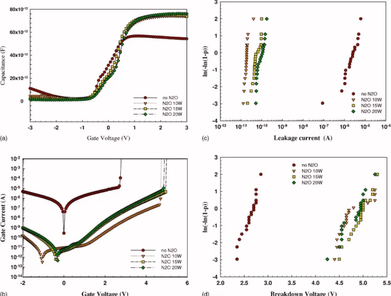
radi-cal introduced in the bulk high-k film. The oxygen profiles for all samples were measured and shown in Fig. 8. It is clear that the sample with N2O plasma treatment exhibited an increased oxygen concentration compared to that the without one. From the previous report,29leakage current of high-k dielectrics with nitrogen incorpo-ration can be significantly reduced by 3-4 orders of magnitude. Re-cently, it has been widely accepted that the reason for leakage cur-rent reduction by nitrogen incorporation is due to that nitrogen anneals oxygen vacancies.37,38As a result, the increase of oxygen by the N2O plasma treatment is also helpful to reduce the oxygen va-cancy in the bulk which is strongly related to the leakage current in high-k dielectrics.34-38,40The electrical results for all samples with or without N2O plasma treatment are shown in Fig. 9. Figure 9a shows the C-V curves for all samples. All capacitors with the N2O plasma
treatment have better-behaved C-V curves than that those without. This implies that the interfacial property has been improved by this N2O plasma treatment.41The accumulation capacitance Cox of all N2O plasma treatment capacitors is higher than on the Coxof those
Figure 6. 共Color online兲 Electrical measurements for samples oxidized at 850°C for 5 min with and without N+ion implantation.共a兲 Gate current vs
gate voltage. 共b兲 Weibull distribution of gate leakage at Vg= 1 V. 共c兲
Weibull distribution of breakdown voltage.
Figure 7. SIMS profiles for samples with 20 W N2O plasma treatment.
Figure 8. 共Color online兲 The oxygen profiles for samples without N2O
plasma or with N2O plasma treatment using powers of 10, 15, and 20 W. G21
without. This is due to the passivation of oxygen and nitrogen, re-sulting in a good interface of the dielectrics with the silicon sub-strate. Figure 9b shows the gate leakage. The N2O plasma-treated sample shows a great improvement compared with the untreated sample. The Weibull distribution of gate leakage and breakdown voltage are shown in Fig. 9c and d, respectively. Capacitors with N2O plasma treatment demonstrate much lower gate leakage
cur-rents and higher breakdown voltages.
Conclusions
We have investigated three approaches to nitrogen incorporation for the new CoTiO3high-k dielectrics. Nitrogen共N2+兲 incorporation
by ion implantation can improve the electrical properties in terms of gate leakage, breakdown voltage, and TBD. To reduce the mass of ion implanting species, N+ ion implantation has been used. The same trends can be found as those produced using N2+. Higher doses of N+ can improve the performance further. An alternative N
2O
plasma treatment was also an excellent method to improve the elec-trical properties, exhibiting better-behaved C-V curves, lower gate leakage currents, and higher breakdown voltages compared with the untreated samples.
Acknowledgment
This work was supported by the National Science Council, Tai-wan, under contract no. NSC-94-2215-E009-071. The authors
ac-knowledge the fabrication support of NDL, Hsinchu, Taiwan. National Chiao Tung University assisted in meeting the publication costs of this article.
References 1. Y. Taur, IBM J. Res. Dev., 46 213共2002兲.
2. S. H. Lo, D. A. Buchanan, Y. Taur, and W. Wang, IEEE Electron Device Lett., 18, 209共1997兲.
3. K. Sekine, Y. Saito, M. Hirayama, and T. Ohmi, IEEE Trans. Electron Devices, 47, 1370共2000兲.
4. M. Khare, G. Xin, X. W. Wang, T. P. Ma, G. J. Cui, T. Tamagawa, B. L. Halpern, and J. J. Schmitt, VLSI Technology, p. 51共1997兲.
5. C. S. Kuo, J. F. Hsu, S. W. Huang, L. S. Lee, M. J. Tsai, and J. G. Hwu, IEEE
Trans. Electron Devices, 51, 854共2004兲.
6. D. S. Yu, C. H. Huang, A. Chin, Z. Chunxiang, M. F. Li, B. J. Cho, and D. L. Kwong, IEEE Electron Device Lett., 25, 138共2004兲.
7. L. Manchanda, W. H. Lee, J. E. Bower, F. H. Baumann, W. L. Brown, C. J. Case, R. C. Keller, Y. O. Kim, E. J. Laskowski, M. D. Morris, R. L. Opila, P. J. Silver-man, T. W. Sorsch, and G. R. Weber, Tech. Dig. - Int. Electron Devices Meet.,
1998, 605.
8. H. Y. Yu, M. F. Li, and D. L. Kwong, IEEE Trans. Electron Devices, 51, 609 共2004兲.
9. J. Lu, Y. Kuo, and J. Y. Tewg, J. Electrochem. Soc., 153, G410共2006兲. 10. W. J. Zhu, T. P. Ma, S. Zafar, and T. Tamagawa, IEEE Electron Device Lett., 23,
597共2002兲.
11. Y. Y. Fan, R. E. Nieh, J. C. Lee, G. Lucovsky, G. A. Brown, L. F. Register, and S. K. Banerjee, IEEE Trans. Electron Devices, 49, 1969共2002兲.
12. I. Kim, J. Koo, J. Lee, and H. Jeon, Jpn. J. Appl. Phys., Part 1, 45, 919共2006兲. 13. C. H. Lee, H. F. Luan, W. P. Bai, S. J. Lee, T. S. Jeon, Y. Senzaki, D. Roberts, and
Figure 9. 共Color online兲 共a兲 C-V curves for all samples with and without N2O plasma treatment.共b兲 Gate leakage current vs gate voltage. 共c兲 The Weibull
D. L. Kwong, Tech. Dig. - Int. Electron Devices Meet., 2000, 27. 14. G. C. F. Yeap, S. Krishnan, and M. R. Lin, Electron. Lett., 34, 1150共1998兲. 15. F. C. Chiu, J. J. Wang, J. Y. M. Lee, and S. C. Wu, J. Appl. Phys., 81, 6911共1997兲. 16. A. Paskaleva, E. Atanassova, and T. Dimitrova, Vacuum, 58, 470共2000兲. 17. T. S. Chao, W. M. Ku, H. C. Lin, D. Landheer, Y. Y. Wang, and Y. Mori, IEEE
Trans. Electron Devices, 51, 2200共2004兲.
18. S. Inumiya, K. Sekine, S. Niwa, A. Kaneko, M. Sato, T. Watanabe, H. Fukui, Y. Kamata, M. Koyama, A. Nishiyama, M. Takayanagi, K. Eguchi, and Y. Tsuna-shima, in IEEE Symposium on VLSI Technology, IEEE, p. 17共2003兲.
19. K. Sekine, S. Inumiya, M. Sato, A. Kaneko, K. Eguchi, and Y. Tsunashima, Tech.
Dig. - Int. Electron Devices Meet., 2003, 103.
20. T. Watanabe, M. Takayanagi, R. Iijima, K. Ishimaru, H. Ishiuchi, and Y. Tsuna-shima, in IEEE Symposium on VLSI Technology, IEEE, p. 17共2003兲.
21. A. Kaneko, Y. Kamata, M. Ono, M. Koyama, A. Nishiyama, Y. Kamimuta, C. Hongo, A. Takashima, D. Gao, S. Inumiya, K. Eguchi, and M. Takayanagi, in
SSDM, p. 742,共2002兲.
22. A. L. P. Rotondaro, M. R. Visokay, J. J. Chambers, A. Shanware, R. Khamankar, H. Bu, R. T. Laaksonen, L. Tsung, M. Douglas, R. Kuan, M. J. Bevan, T. Grider, J. McPherson, and L. Colombo, in IEEE Symposium on VLSI Technology, IEEE, p. 148共2002兲.
23. A. Shanware, J. McPherson, M. R. Visokay, J. J. Chambers, A. L. P. Rotondaro, H. Bu, M. J. Bevan, R. Khamankar, and L. Colombo, Tech. Dig. - Int. Electron
Devices Meet., 2001, 137.
24. J. C. Wang, D. C. Shie, T. F. Lei, and C. L. Lee, Electrochem. Solid-State Lett., 6, F34共2003兲.
25. M. Koyama, A. Kaneko, T. Ino, M. Koike, Y. Kamata, R. Iijima, Y. Kamimuta, A. Takashima, M. Suzuki, C. Hongo, S. Inumiya, M. Takayanagi, and A. Nishiyama,
Tech. Dig. - Int. Electron Devices Meet., 2002, 849.
26. C. S. Kang, H. J. Cho, K. Onishi, R. Choi, Y. H. Kim, R. Nieh, J. Han, S. Krishnan, A. Shahriar, and J. C. Lee, Tech. Dig. - Int. Electron Devices Meet., 2002, 865.
27. H. S. Jung, Y. S. Kim, J. P. Kim, J. H. Lee, J. H. Lee, N. I. Lee, H. K. Kang, K. P. Suh, H. J. Ryu, C. B. Oh, Y. W. Kim, K. H. Cho, H. S. Baik, Y. S. Chung, H. S. Chang, and D. W. Moon, Tech. Dig. - Int. Electron Devices Meet., 2002, 853. 28. Y. Morisaki, T. Aoyama, Y. Sugita, K. Irino, T. Sugii, and T. Nakamura, Tech. Dig.
- Int. Electron Devices Meet., 2002, 861.
29. C. H. Choi, S. J. Rhee, T. S. Jeon, N. Lu, J. H. Sim, R. Clark, M. Niwa, and D. L. Kwong, Tech. Dig. - Int. Electron Devices Meet., 2002, 857.
30. D. Ishikawa, S. Sakai, K. Katsuyama, and A. Hiraiwa, Tech. Dig. - Int. Electron
Devices Meet., 2002, 869.
31. H. J. Cho, C. S. Kang, K. Onishi, S. Gopalan, R. Nieh, R. Choi, S. Krishnan, and J. C. Lee, IEEE Electron Device Lett., 23, 249共2002兲.
32. N. J. Seong, S. G. Yoon, S. J. Yeom, H. K. Woo, D. S. Kil, J. S. Roh, and H. C. Sohn, Appl. Phys. Lett., 87, 132903共2005兲.
33. T. M. Pan, T. F. Lei, and T. S. Chao, J. Appl. Phys., 89, 3447共2001兲. 34. T. M. Pan, T. F. Lei, T. S. Chao, K. L. Chang, and K. C. Hsieh, Electrochem.
Solid-State Lett., 3, 433共2000兲.
35. S. Kamiyama, T. Miura, Y. Nara, and T. Arikado, J. Electrochem. Soc., 152, G750 共2005兲.
36. K. J. Choi, J. H. Kim, and S. G. Yoon, Electrochem. Solid-State Lett., 7, F59 共2004兲.
37. J. L. Gavartin, A. L. Shluger, A. S. Foster, and G. I. Bersuker, J. Appl. Phys., 97, 053704共2005兲.
38. S. A. Krishnan, M. Quevedo, R. Harris, B. H. Lee, G. Bersuker, and J. C. Lee, Jpn.
J. Appl. Phys., Part 1, 45, 2945共2006兲.
39. M. Bhat, D. J. Wristers, L. K. Han, J. Yan, H. J. Fulford, and D. L. Kwong, IEEE
Trans. Electron Devices, 42, 907共1995兲.
40. N. Umezawa, K. Shiraishi,, T. Ohno, H. Watanabe, T. Chikyow, K. Torii, K. Yam-abe, K. Yamada, H. Kitajima, and T. Arikado, Appl. Phys. Lett., 86, 143507 共2005兲.
41. S. Chakraborty, M. K. Bera, and C. K. Maiti, J. Appl. Phys., 100, 023706共2006兲. G23