This content has been downloaded from IOPscience. Please scroll down to see the full text.
Download details:
IP Address: 140.113.38.11
This content was downloaded on 28/04/2014 at 10:53
Please note that terms and conditions apply.
The Effects of Shallow Germanium Halo Doping on N-Channel Metal Oxide Semiconductor
Field Effect Transistors
View the table of contents for this issue, or go to the journal homepage for more 1999 Jpn. J. Appl. Phys. 38 L33
(http://iopscience.iop.org/1347-4065/38/1A/L33)
Jpn. J. Appl. Phys. Vol. 38 (1999) pp.L33–L34 Part 2, No. 1A/B, 15 January 1999
c
°1999 Publication Board, Japanese Journal of Applied Physics
The Effects of Shallow Germanium Halo Doping on N-Channel Metal
Oxide Semiconductor Field Effect Transistors
Meng-Fan WANG1, Chao-Hsin CHIEN1, Tien-Sheng CHAO2, Horng-Chih LIN2, Fuh-Cheng JONG1, Tiao-Yuan HUANG1,2and Chun-Yen CHANG1
1Department of Electronics Engineering & Institute of Electronics, National Chiao Tung University, Hsinchu, 300, Taiwan 2National Nano Device Laboratories, Hsinchu, 300, Taiwan
(Received December 4, 1997; accepted for publication November 4, 1998)
In this paper, we report the use of shallow germanium halo doping on improving the short-channel effects of deep submicron n-channel metal-oxide-semiconductor field effect transistors. It is demonstrated that by adding a shallow (i.e., 10 keV) germa-nium large-angle-tilt implant (LATID), Vthlowering in short-channel transistors is significantly improved. The improvement is
found to increase with increasing germanium dose. A low germanium dose (e.g., 5× 1012cm−2) is also found to effectively
improve the drain-induced barrier lowering (DIBL) of the short-channel transistors. Our results also show that junction leakage degradation, which has been previously reported to accompany germanium implants using higher energy, can be minimized by the shallow low-dose implant used in this study.
KEYWORDS: germanium halo implant, large-angle-tilt implant, short-channel effects, drain-induced barrier lowering, threshold-voltage lowering
L33
1. Introduction
Germanium has been applied for improving the short-channel effects of n-short-channel metal-oxide-semiconductor field effect transistors (MOSFETs) by retarding the diffusion of the source/drain dopants.1–3)In those studies, a high implant
en-ergy (i.e., 125 keV) and high dose (i.e., 5× 1015cm−2) were
used, which resulted in the extension of the Ge-doped region beyond the metallurgical junction, causing severely degraded junction leakage characteristics.4)Recently, the reverse
short-channel effects (RSCE), which involve a delay or even an in-crease in threshold voltage lowering, have received signifi-cant attention.5–8) The RSCE has been attributed to the
lat-eral redistribution of the dopant near the source/drain junc-tion. This lateral redistribution is ascribed to the crystal de-fects formed during post-source/drain implant anneal. In this study, we employ a very shallow (i.e., 10 keV) germanium im-plant through large-angle-tilt imim-plant (LATID)9)(i.e., 60◦) to form very shallow halo regions abutting the source-drain re-gions. We demonstrate that the incorporation of such a shal-low germanium is also effective in improving the threshold voltage (Vth) lowering and the drain-induced barrier lowering
(DIBL) characteristics of the transistors, while maintaining a low leakage junction.
2. Experiments
N-channel MOSFETs were fabricated on 6-inch p-type (100) 15–25Ä-cm silicon wafers. After active area definition by local oxidation of silicon (LOCOS), Vth-adjustment and
anti-punch-through implants were performed using BF+2 and boron implants, respectively. Thin gate oxides were grown in dry oxygen at 900◦C, followed by a deposition of 2000 Å-thick polysilicon at 620◦C. The plasma resist ashing was employed to achieve the desired short gate length. After polysilicon etching, wafers were split to receive a shallow (i.e., 10 keV) Ge halo implant through 60◦-tilt LATID with various doses. Next, shallow (i.e., extended) and deep S/D regions were formed by 10 keV arsenic implant with 4× 10¹⁴
and 1× 1015cm−2doses, respectively. A 150-nm
tetra-ethyl-ortho-silicate (TEOS) sidewall spacer was formed between the two implants. Finally, a 800◦C, 30 min furnace anneal and
in Fig. 3), compared to that of the non-Ge control is observed, suggesting that the leaky junction reported in previous litera-ture in the case of high-energy implants can indeed be mini-mized by employing a shallow Ge halo implant with proper dose. For the 1× 10¹⁴/cm2 split, however, the area junction leakage current increases more dramatically, suggesting that defects created by such a heavy Ge implant can no longer be fully annealed at the reduced thermal cycle as required for deep submicron processing. Nevertheless, the peripheral junction leakage current (i.e., the slope in Fig. 3) does not increase even for the highest Ge dose of 1× 1014cm−2.
The transistor off-state leakage current (measured at gate voltage of 0 V and a drain voltage of 2.5 V) is shown in Fig. 4. It is observed that at low Ge halo dose, the off-state leakage channel behaviors, including reduced threshold-voltage low-ering and improved DIBL effects.
The reverse leakage current as a function of periphery over area ratio (P/A) is shown in Fig. 3 for n+/p diodes. For low Ge doses, i.e., 5×10¹²and 1×1013cm−2, only a minimal increase
in area leakage current (i.e., the interception with vertical axis a 1050◦C, 10 s rapid thermal anneal (RTA) were performed to activate the dopants.
The effects of the Ge halo dose on Vth lowering are
de-picted in Fig. 1. It can be seen that while the non-Ge control devices display severe threshold voltage lowering for chan-nel length smaller than 1µm, Vth lowering is significantly
alleviated with the Ge halo implant. Although the improve-ment increases with increasing Ge dose, it approaches sat-uration for Ge doses higher than 1× 1013cm−2. This
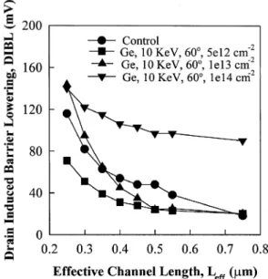
im-provement can be explained by the reduced lateral diffusion of dopant near the S/D region, since Ge is known to retard dopant diffusion.4)The DIBL effects are measured as a
func-tion of channel length and plotted in Fig. 2. The device with light Ge dose (i.e., 5× 1012cm−2) shows improved DIBL, especially for shorter devices. However, for the device with 1× 1013cm−2 Ge dose, although DIBL is reduced for chan-nel length longer than 0.35µm, DIBL deteriorates for shorter devices. While for the device with the highest Ge dose used in this study (i.e., 1× 1014cm−2), DIBL is degraded for all
channel lengths. From these results, it can be concluded that a light Ge halo implant can be used to achieve optimum
short-L34 Jpn. J. Appl. Phys. Vol. 38 (1999) Pt. 2, No. 1A/B M.-F. WANGet al.
of the Ge-implanted device is indeed significantly improved over the non-Ge control device, suggesting that a light Ge halo implant can be applied to reduce the off-state leakage current of the resultant transistor, due to the improved DIBL effects.
3. Conclusion
The effects of an ultra shallow germanium halo implant have been investigated. Our results indicate that by employ-ing a shallow 10 keV Ge halo region through the large-angle-tilt implant, Vth roll-off improves with increasing Ge halo
dose. The DIBL effects are also improved with light Ge halo implant (e.g., 5× 1012cm−2), although at higher doses DIBL effects actually worsen. Junction leakage degradation, which is known to accompany Ge implants as reported in previous literature, can also be effectively minimized by employing the shallow Ge implant used in this study. N-channel transistors with improved off-state leakage current can thus be obtained.
Acknowledgment
The authors would like to thank National Nano Device Laboratories for wafer processing. This work was partly supported by the R.O.C.’s National Science Council through contracts #NSC86-2722-2317-001, and #NSC85-2215-E009-039.
1) J. R. Pfiester, M. E. Law and R. W. Dutton: IEEE Electron Dev. Lett. 9 (1988) 343.
2) M. C. Ozturk, J. J. Wortman, C. M. Osburn, A. Ajmera, G. A. Rozgonyi, E. Frey, W. K. Chu and C Lee: IEEE Trans. Electron Dev. 35 (1988) 659. 3) J. R. Pfiester and J. R. Alvis: IEEE Electron Dev. Lett. 9 (1988) 391. 4) D. S. Wen and S. H. Goodwin-Johansson: IEEE Trans. Electron Dev. 35
(1988) 1107.
5) C. Mazure and M. Orlowski: IEEE Electron Dev. Lett. 10 (1989) 556. 6) H. I. Hanafi, W. P. Nobel, R. S. Bass, K. Varahramyan, Y. Lii and A. J.
Dally: IEEE Electron Dev. Lett. 12 (1993) 575.
7) H. Jacobs, A. V. Schwerrin, D. Scharfetter and F. Lau: in IEDM Tech. Dig. (1993) 307.
8) C. Y. Chang, C. Y. Lin, J. W. Chou, C. H. Hsu, H. T. Pan and J. Ko: IEEE Electron Dev. Lett. 11 (1994) 437.
9) T. Hori: in Symp. VLSI Tech. Dig. (1988) 15. Fig. 1. Threshold voltage roll-off as a function of channel length for
con-trol devices and devices with various germanium halo implant doses.
Fig. 4. Off-state leakage current of control devices and devices with var-ious germanium halo implant doses. The effective channel length is 0.25µm and off-state leakage current is measured at a gate voltage of 0 V and a drain voltage of 2.5 V.
Fig. 3. Diode leakage current density as a function of periphery over area (P/A) ratio. Leakage current is measured at a reverse biased voltage of 3.3 V.
Fig. 2. Drain-induced-barrier-lowering as a function of channel length for control devices and devices with various germanium halo implant doses.