Microsystem Technologies 4 (1998) 66—69( Springer-Verlag 1998
High precision, low cost mask for deep x-ray lithography
B.-Y. Shew, Y. Cheng, W.-P. Shih, M. Lu, W.H. Lee
Abstract The precision of transferred patterns are highly dependent on the quality of the mask in deep x-ray lithogra-phy. Many parameters, such as the critical energy of the synchrotron light, beamline optics and even the microstructure to be exposed should be considered in mask design. In this paper, the design rules and the boundary conditions for deep x-ray mask are discussed in general. The method of making a precision, multilayer mask using UV lithography technique is also described.
1
Introduction
In deep x-ray lithography, the high intensity and highly collimated synchrotron radiation is used as the light source for exposure. The spectrum of the radiation ranges from UV light to hard x-ray (Winick, 1980). Generally speaking, more hard x-rays are created as the energy of the stored electrons in the accelerator is increased. The light near the hard x-rays are selected to provide the depth of exposure in deep x-ray lithography. It is not easy to vary the electron energy for selecting proper photon energy. Instead, the filters of the beamline optics could be adjusted. Beryllium or polymer windows are normally used as the high-pass filters, whereas the low-pass filter is accomplished by the reflection mirror or a window with a special coating (Cheng, Shew et al., 1997).
Via x-ray lithography, the pattern is transferred onto the photoresist through the mask which contains mainly two parts, i.e. membrane and absorber (Bowden, 1994). The membrane must be transparent to x-rays. Materials with low atomic numbers and low densities, such as Be, Si, Ti, BN, Si3N4 or SiC,
Received:25August1997/ Accepted:3September1997 B.-Y. Shew, Y. Cheng
Synchrotron Radiation Research Center No. 1 R&D Road VI, SPI Park, 30077, Hsinchu, Taiwan, R.O.C.
W.-P. Shih
National Tsing Hua University, Hsinchu, Taiwan, R.O.C. M. Lu
National Chiao Tung University, Hsinchu, Taiwan, R.O.C. W.H. Lee
National Taiwan University, Taipei, Taiwan, R.O.C.
Supported by the National Science Council (NSC 85-2622-E007-010) and (NSC 85-2215-E-213-001)
are frequently used to make the membrane. They should not only be dimensionally stable to keep the precision of the defined pattern but also have sufficient mechanical strength for handling. The absorber must efficiently attenuate incident x-rays to provide contrast on the resist. Metals with high atomic number and high densities, such as Au, Ta, W or Pb are utilized as x-ray absorbers. The absorber should have low defect density. The photoelectrons generated from incident x-rays have better to be prevented from resist.
The high precision mask for deep x-ray lithography was made by two steps previously (Ehrfeld et al., 1986). In the first step, pattern is generated by e-beam writer. Then gold is plated between the developed structures to form an ‘‘intermediate’’ mask. Since the penetration depth of electrons is relatively low, synchrotron x-rays are used as the exposure source to enlarge the depth of absorber from the intermediate mask in the second step. This method is complex and expensive. An extra x-ray beamline is required.
The electron energy of Taiwan Light Source (TLS) at the SRRC is 1.5 GeV. The critical photon energy and its critical wavelength are 2.3 keV and 0.54 mm respectively (Cheng, 1996). Since no mirror is employed in the micromachining beamline in the SRRC, the required thickness of the photo-absorber has to be increased to reduce the back-scattered electrons on the substrate (Cheng, Shew et al., 1997). According to our calculation, disregarding the effect of back-scattered electrons, a 10lm gold absorber is required to make microstructures of 300lm height (Shih et al., 1997 and Cheng, Kuo, Su, 1997). A thicker Structure requires a thicker absorber, even if the multiple exposure process is applied. However, it is difficult to plate such a thick layer without losing precision.
In this report, a mask structure with multilayer absorber is reported to solve the problem. The top gold layer is designed to defined the edge of the structure accurately, whereas the second layer is used to stop penetration of the hard x-rays. Since the thickness of the plated gold layer is reduced, the precision of the mask could be enhanced even though wet etching causes undercut at the second layer. The high precision, low cost absorber structure could be used both on contact mask and conformal mask for deep x-ray lithography.
2
Multilayer design
Many materials could fulfill the required properties of an absorber. However, only general issues of mask design are to be discussed in this section. Suppose that we have a multilayer
1 2 3
Substrate
Fig. 1. Schematic multilayer structure of deep x-ray mask
structure as shown in Fig. 1 and all of the layers have a good adhesion in between. The following characters of the materials should be considered from the aspect of deep x-ray litho-graphy:
1. Absorption coefficient of x-rays 2. Absorption coefficient of fluorescence 3. Thermal expansion coefficient 4. Extensibility
5. Thermal conductivity 6. Mechanical strength 7. Oxidation stability
The first three characters should be varied from layer to layer, whereas the later four characters should be kept at good qualities in each layer. Generally speaking, the criteria below should be met:
1. The bottom layer should have a low absorption coefficient of x-rays and a high absorption coefficient of fluorescence such that the induced secondary electrons and fluorescence could be prevented from the resist.
2. One of the layers should be carefully made to transfer pattern in precision. The other layers, except the membrane, should have a geometrical shrinkage not to destroy the defined edge.
3. In the optimal conditions, the thermal expansion coefficient should change slowly from layer to layer.
Although there are many possibilities to manufacture the mask according to the mentioned criteria, the low cost methods including UV lithography, wet etching, dry etching, plating, and sputtering were mainly addressed in this paper.
3
Contact mask
For the contact mask, the substrate shown in Fig. 1 is the membrane. In this report, silicon nitride was used as the membrane material because of its high Young’s modulus, low thermal expansion coefficient and low absorbing coefficient of x-rays.
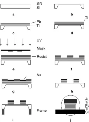
Figure 2 is a schematic for making a contact mask. Silicon nitride was first deposited on silicon wafer (Fig. 2a) by LPCVD technique. The residue stress in the nitride films can be carefully controlled by oxidation (Chou et al., 1996). A window was then opened on one side (back side) of the substrate (Fig. 2b) before oxidation. The backside etching is accomp-lished by two steps to prevent top side etching (Petzol, 1988).
Fig. 2a–j. Manufacturing procedure for contact mask
A Ti/Pb/Ti sandwich structure was sputtered subsequently on the top side of the substrate as shown in Fig. 4c and 4d. The bottom titanium film served as an adhesion layer between the silicon substrate and lead absorber, and the top titanium was used to prevent oxidation of lead in the atmosphere. The top titanium layer was chemically treated (0.5 M NaOH, 0.2 M H2O2) for minutes at room temperature to form a thin TiOx film on the surface (Mohr et al., 1988). TiOx is conductive and can serve as a plating base in the subsequent process. Moreover, the fine structure of the TiOx can also improve adhesion with gold absorber by mechanical interlocking.
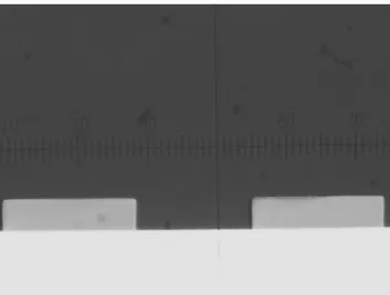
After those steps mentioned above, resist (negative-type, THB-37, JSR company, Japan) was then spin coated on the top side of the substrate and patterned by UV lithography as illustrated in Fig. 2e and 2f. The parameters of resist process, including spin rates, bake temperatures and developing condition, were optimized and a resolution of 1lm was achieved with a resist thickness of 32lm (Fig. 3). The gold absorber was subsequently plated through the resist structure (Fig. 2g). The necessary thickness of gold was theoretically calculated according to the exposure depth as indicated in Fig. 4 (Shih et al., 1997). The photoresist and Ti/Pb/Ti were subsequently stripped. The remaining silicon on the back side was also etched by chemicals (Fig. 2h). Finally, the silicon wafer is glued on a glass holder as shown in Fig. 2i.
Fig. 2j is a diagram revealing the multilayer absorber structure after these processes. The gold was used to define the transferred pattern. Since the lead layer could help absorbing hard x-rays, the necessary thickness of the gold absorber could be reduced. The accuracy could be kept during gold electro-plating. In addition, the lead layer would not disturb the edge
Fig. 3. Photoresist of 32km height and 100 km width after UV lithography 0 2 4 6 8 10 12 14 16 18 0 100 200 300 400 500 Exposure depth (µm) R equi red t h ickness of gol d absor ber (µ m )
Fig. 4. Calculated relationship between exposure depth and required gold thickness
defined by gold because undercut happened during isotropic etching.
4
Conformal mask
For the conformal mask, the substrate shown in Fig. 1 is the x-ray photoresist, such as PMMA. The major problem involved here is to create a thin metal layer on resist with good adhesion in between. Many methods have been tested and succeeded in chemical plating of copper. Figure 5 is the manufacturing procedure for a multilayer conformal mask for deep x-ray lithography. The PMMA sheet was plasma treated before chemical plating to provide better wettability and proper surface roughness. As shown in Fig. 5a, the copper-coated PMMA sheet was glued to the substrate. The layered absorbers were then deposited on the PMMA following the processes in making contact mask (Fig. 5b—f ). Fig. 6 is the fabricated multilayerd leadframe conformal mask for the x-ray deep lithography.
This design also provides a very important feature for the multiple-exposure process. Since the volume of unexposed PMMA might change when absorbing the developer, the extensible lead layer will reduce the deformation of the gold absorber however. Cu foil PMMA Substrate Ti Pb UV Mask Resist Au a e c b f d
Fig. 5a–f. Manufacturing procedure of conformal mask for deep x-ray lithography
Fig. 6. Multilayer conformal mask for deep x-ray lithography
5 Summary
The methods to make a high precision, multilayer mask for deep x-ray lithograhy are presented. The manufacturing process is simple and of low cost. The mask contains many good features during x-ray processing and the designed structure could be used both in contact and conformal x-ray masks.
References
1. Winick H:(1980) Properties of synchrotron radiation. Winick, H.; Donach, S.; ‘‘ed’’ Synchrotron Radiation Research, New York, Plenum Press, ch. 2, p. 11—p. 25
2. Cheng Y; Shew B-Y; Shih W-P; Wang SS; Lin CY; Yang W-K; Lu M; Lee
WH:(1997) Micromachining program status at the SRRC, Harmst 97,
Microsystem Technologies, printing
3. Bowden MJ:(1994) Introduction to microlithography, chap. 2, p. 120—132, 2nd edition, Washington DC, ACS Profesional Reference Book
4. Ehrfeld W; Glashauser W; Munchmeyer D; Sshejb W:(1986) Mask making for synchrotron radiation lithograh, Microelectronic Eng., 5, p. 463—470
5. Shih W-P; Shew BY; Cheng Y; Hwant G-J:(1997) Dosage modeling for deep x-ray lithography application, Harmst 97, Microsystem Technologies, printing
6. Cheng Y:(1996) LIGA activity in Taiway, Microsystem Technologies 2, p. 157—161, Springer-Verlag
7. Cheng Y; Kup N-Y; Su CH:(1997) Dose distribution of synchrotron x-ray penetrating materials of low atomic numbers. Review of Scientific Instruments, Vol. 68, No. 5,
p. 2163—p.2166
8. Chou BCS; Chen C-N; Shie J-S:(1996) A method of fabricating a thin, and low stress dielectric film for microsensors applications. Eurosensors X, Leuven, Belgium, p1.1—173
9. Petzold H-C:(1988) X-ray lithography. Proceedings of the CCAST Symposium, Beijing, China, p. 277—370
10. Mohr J; Ehrfeld W; Mu¨nchmeyer D:(1988) Analyse der defektur-sachen und der genauigkeit der strukturubertagung bei der Ro¨ntgentiefen-lithographie mit synchrotronstrahlung, KfK-Bericht 4414, p. 71, Kernforschungszentrum, Karlsruhe