Growth of diamond nanoplatelets on nanocrystalline diamond substrates
Hou-Guang Chen
a,⁎
, Li Chang
ba
Department of Materials Science and Engineering, I-Shou University, Kaohsiung 840, Taiwan b
Department of Materials Science and Engineering, National Chiao Tung University, Hsinchu 300, Taiwan
a b s t r a c t
a r t i c l e i n f o
Available online 24 November 2008 Keywords:
Nano-diamond MPCVD TEM Field emission
We report the growth of single crystalline diamond nanoplatelets (DNPs) on different types of nano-crystalline diamond substrates by high temperature microwave-plasma chemical vapor deposition. The influence of methane concentration on DNP morphologies has been studied. According to high-resolution transmission electron microscopy observation, DNPs are typical tabular twined crystallites which consist of several twin lamellae parallel to platelet surfaces and the side-face structure of DNPs is the ridge-and-trough structure consisting of {100} and {111} faces. Thefield emission properties of DNPs with various mor-phologies and nano-crystalline diamond substrates were characterized. The turn-on electricalfield of DNPs with well-faceted side edges was lower in comparison with the DNPs with irregular shapes and nano-crystalline-diamond substrate.
© 2008 Elsevier B.V. All rights reserved.
1. Introduction
Diamondfilm growth by chemical vapor deposition (CVD) has been widely demonstrated for almost two decades, due to its unique physical and chemical properties, such as wide band gap, negative electron affinity, chemical inertness, excellent mechanical properties, and the highest thermal conductivity in room temperature. Recently, various diamond-based nanostructural materials have attracted intensive research interests and regarded as a new material with great potentiality in various applicationfields such as, biomedical, electronic, and optoelectronic devices [1–5]. For instance, nano-diamond biomedical sensors and biolabeling technique have been proposed[2]. Due to its negative or low electron affinity characteristics, nano-diamond and other carbon based materials also have fascinating electron emission properties and made them the candidate materials for electron emitter. The fabrication of stable and robust electron emission cathodes consisting of nano-crystalline diamond (NCD)films forflat-panel display or electron beam emitter has been increasingly demonstrated from many research groups[5–6].
Nanostructured materials can effectively extend and enhance the properties. Thus, the electron emission performance of diamond also can be enhanced through nanostructured diamond. Recently, great efforts have been devoted to synthesize nanodiamonds in different structures. Several authors attempt to fabricate diamond nanopillar or nanowhisker by plasma etching or by growth on anodic aluminum oxide templates[7–9]. Thefield emission characteristics of various diamond nanostructures have been widely demonstrated. Tzeng et al. proposed
that NCDs grown on silicon nanowire template performedfield emission properties comparable with those of the carbon nanotubes[10]. In our pervious studies, regular hexagonal single crystalline diamond nano-platelets (DNPs) grown on poly-crystalline diamond substrates, silicon and nanocrystalline diamond (NCD) substrates can be obtained through high-temperature microwave plasma enhanced chemical vapor deposi-tion (MPCVD)[11–15]. In earlier work, we found that NCD substrates and high-temperature plasma might play an important role on DNP growth. However, the effect of NCD on the growth of DNPs is unclear. In order to clarify the effect of diamond nano-crystallites on the nucleation of DNPs, here we used different types of nano-crystalline diamonds (NCD) as substrate for DNP growth. Furthermore, somefield emission character-istics of the diamond nanoplatelets grown on NCD substrates have also been demonstrated.
2. Experimental
Growth of NCD substrates and DNP was carried out in a 2.45 GHz ASTeX-type microwave plasma CVD reactor equipped with a 1.5 kW microwave generator. Hydrogen and methane mixture was activated by microwave. In this paper, the two types of NCDfilms were used as substrates for DNP growth: continuous NCDfilm (designated as c-NCD) and discontinuous diamondfilm (designated as d-NCD). For c-NCD film deposition, negative bias enhanced nucleation (NBE) has been implemented on the bare Si substrates to assure a homogeneous and high nucleation density. During c-NCD deposition, 200 V negative bias was applied on the substrate to enhance diamond nucleation. The gas flow was 9 and 291 sccm for CH4and H2, respectively, and the pressure
was kept at 20 Torr in the deposition period. For d-NCD deposition, surface pretreatment of Si substrates was carried by ultrasonic abrasion of nanodiamond powder suspension before deposition. In
⁎ Corresponding author.
E-mail address:[email protected](H.-G. Chen).
0925-9635/$– see front matter © 2008 Elsevier B.V. All rights reserved. doi:10.1016/j.diamond.2008.11.010
Contents lists available atScienceDirect
Diamond & Related Materials
addition, no negative bias was involved during deposition. Following NCD growth, both of NCDfilm substrates were loaded into the reac-tor for DNP growth. DNPs were deposited under high temperature plasma conditions (above 1100 °C) which can be achieved through increasing plasma power (1000 W) and process pressure (60 Torr). Furthermore, the influence of methane concentration on DNP growth was examined.
After deposition, the surface morphology was examined using a field-emission scanning electron microscope (SEM) (JEOL JSM-6500F at 10 kV). The nanoplatelets were further characterized by transmis-sion electron microscopy (TEM). A Philips Tecnai 20 TEM was em-ployed for image observation and selected-area diffraction (SAD) analyses. Furthermore, in order to analyze the details about the micro-structure of diamond nanoplatelets, high-resolution transmission
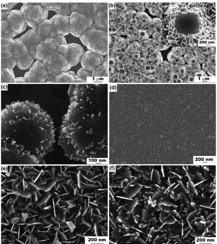
Fig. 1. (a) SEM image of as-grown d-NCD substrate. (b) A large number of nanoplatelets grown on diamond balls at 1% CH4concentration for 15 min high temperature plasma growth. Inset shows enlarged image of the nanoplatelets grown on one of the diamond balls. (c) The nanoplatelets grown at the peripheral region of the sample. (d) Image of as-grown c-NCD substrate. Nanoplatelets grown on c-NCD substrates (e) at 1% CH4concentration for 30 min and (f) at 3% CH4concentration for 15 min, respectively.
electron microscopy (HRTEM) was performed in a JEOL-2010F micro-scope. The TEM specimens were thinned by conventionally mechani-cal process, followed by Ar+ ion beam milling. The
field emission properties were examined at ~10− 7Torr. An indium-tin oxide coated glass was used as anode which was placed 60 µm above the sample surface. The measurements of emission current density were per-formed by using a Keithley 237 source measure unit.
3. Results and discussion
3.1. Diamond nanoplatelets grown on d-NCD and c-NCD substrates Thefilm morphologies of as-grown d-NCD films can be seen in
Fig. 1(a). The d-NCD grown on substrate subjected by nanodiamond powder abrasion exhibits discontinuous balls incompletely covered with some {001} facets. For further DNP growth, high temperature plasma growth was performed at 1% CH4concentration for 15 min.
SEM inFig. 1(b) shows that a large number of nanoplatelets grow on diamond balls. In high-magnification SEM observations, nanoplatelets exhibit regular faceting, and several platelets have shapes in hexagon, as shown in the insert ofFig. 1(b). The thickness of each platelet is several tens nanometers. The platelet length is approximately 100– 150 nm. Interestingly, the growth of nanoplatelets on {001} face regions has been suppressed. It is noted that the density of nanoplatelets at the peripheral region of the sample is relatively lower as seen inFig. 1(c), probably resulting from the temperature gradient and non-uniform distribution of active species in the plasma. Nevertheless, well-faceted nanoplatelets in hexagon-like shape can be grown on d-NCD balls.
In Fig. 1(d), the c-NCD films deposited with the BEN process exhibit continuous non-faceted structure composed of several clusters. The growth of nanoplatelet was implemented on c-NCD substrates using the same growth condition on d-NCD substrate as mentioned above. After 30 min growth, high density nanoplatelets with well-faceted morphologies have uniformly grown over the whole c-NCD substrates, as shown inFig. 1(e). However, growth with higher methane concentration (3%) leads to the nanoplatelets in irregular saw-like appearance on their edges, as shown inFig. 1(f), which might be caused by the defects formed in strongly secondary nucleation at high CH4concentration conditions.
3.2. TEM characterization of DNPs grown on c-NCD substrates In order to directly examine the nanoplatelets grown on c-NCD diamond, the sample grown at lower methane concentration (1%) for 30 min was characterized by transmission electron microscopy in cross section. The brightfield (BF) image of the nanoplatelets grown on c-NCD substrate is shown inFig. 2(a). Nanoplatelets with well-faceted appearance or hexagonal shapes were uniformly grown on c-NCDfilm and oriented in random directions. In addition, some needle-like deposits were still nanoplatelets which were oriented parallel to the viewing direction. In order to investigate the microstructure of nanoplatelets in detail, we selected a nanoplatelet which can be tilted to be in edge-on orientation for further observation.Fig. 2(b) shows the darkfield image of the nanoplatelet of 10 nm thickness grown on the c-NCD film. Fig. 2 (c) shows the corresponding selected area electron diffraction pattern of the c-NCDfilm and the nanoplatelet. Besides the ring pattern contributed from c-NCD substrate, the spot pattern inFig. 2 (c) is in consistence with that of cubic twinned diamond inb110N orientation. Thus, it is evident that the nanoplate-lets grown on c-NCD substrates are diamond single crystals. The averaged grain size of c-NCDfilm estimated from the dark field image, inFig. 2(b) is about several tens of nanometers. According to the diffraction pattern and dark field image, the twin lamellae with several nanometers in thickness are parallel to platelet and hence the main tabular planes of DNPs are diamond {111} planes.
The detail side face structure of DNPs has been investigated by HRTEM.Fig. 3shows the HRTEM image of the side-face structure of a DNP. According to HRTEM observation, the DNPs are typical tabular twinned crystallites which consist of several twin lamellae parallel to platelet surfaces. Remarkably, the side-face structure of DNPs is the ridge-and-trough structure consisting of {100} and {111} faces adjacent to multi-parallel twin planes. Similar side edges can be usually found in noble metals or silver halides twinned platelets
Fig. 2. (a) Cross-sectional TEM brightfield image of nanoplatelets grown on c-NCD substrate. (b) Darkfield image showing the DNP and c-NCD substrate and (c) the corresponding electron diffraction patterns of the c-NCD and DNP.
[16,17]. The mechanism of fast lateral growth through {100}/{111} side face structures, resulting in the anisotropic growth for twinned tabular crystallite formation, has been well established in the case of silver halides platelets[17,18]. The {100}/{111} ridge-and-trough side faces adjacent to twinned planes can provide preferential sites for the nucleation of new layers for lateral crystal growth. The enhanced lateral growth of the crystals is attributed to this self-perpetuating side face geometry. The detailed lateral growth mechanism of diamond nanoplatelet has been discussed elsewhere[12].
TEM characterization verifies that DNPs contain several twin lamellae parallel to platelet. As mentioned above, the multi-parallel twins play a crucial factor for the growth of DNP. NCD initially formed on silicon substrate before DNP growth. Thus, it is speculated that a large quantity of defects incorporated in NCDfilms, for in-stance twins, might provide routes for diamond platelet growth. Interestingly, for DNPs grown on d-NCD substrates, the diamond nanoplatelets grow selectively on regions where {100} facets do not appear, as shown in the insert ofFig. 1(b). It has been shown that {100} sectors of CVD grown diamond usually have low densities of defects, in particular twins[19]. Thus, the distribution of the defects containing in diamond substrate can significantly affect the growth position of DNPs.
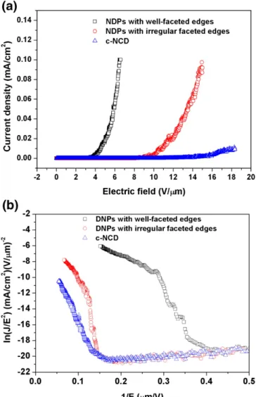
3.3. Thefield emission characteristics of diamond nanoplatelets Thefield emission properties of c-NCD film and DNPs grown on c-NCD at low and high methane concentration conditions were measured to understand if DNPs' edges can be acted as emitters.Fig. 4(a) shows the current density versus electricfield (J–E) characteristics of c-NCD and DNPs with well-faceted and irregular side edges. In this study, the turn-on field was designated as the electric field under which a 10 µA/cm2current
density appeared. The turn-on electricfield of c-NCD substrate is 19 V/µm. However, the samples of DNP grown c-NCD substrate show lower turn-on fields which are 4.58 V/µm and 10.6 V/µm for DNPs with well-faceted and irregular faceted edges, respectively. The turn-on electricfield of the DNP sample with well-faceted edges was lower in comparison with the DNP samples with irregular shapes and c-NCD substrate. The Fowler– Nordheim (F–N) plots of the three samples are depicted inFig. 4(b). The drastic reduction in the F–N slope for the sample of DNPs with well-faceted edges suggests the presence of strongfield emission enhancement
factor in the sample. Field emission can be significantly affected by geometrical factor. Hence, the enhancement of field emission is closely related to the ridge edges of nanoplatelet, as observed by HRTEM shown inFig. 3. The DNPs grown on NCD substrate introduces a geometry which may enhance the field emission properties. However, the samples of DNPs with irregular faceted edges perform field emission at high threshold voltage. The large number of pro-trusions on the side edges of nanoplatelets can play electron emission sites, but high density of emission sites might degrade the field emission characteristics as a result of the screening effect. Therefore, the optimized control of side edge structures, sizes, and densities of DNPs is crucial for highfield emission performance.
4. Conclusion
Diamond nanoplatelets grown on different nanocrystalline dia-mond substrates have been demonstrated in this study. DNP is {111} diamond twinned tabular crystallite, as verified by TEM characteriza-tion. The multi-parallel twin planes in DNP are believed to be a crucial factor for DNP growth under high temperature plasma environment. The high density of defects, especially multiple twins, originally existing in nanocrystalline diamond substrates favors uniform DNP growth. The preliminarilyfield emission properties of DNPs were also demonstrated. Field emission performance can be significantly enhanced through DNP growth.
Fig. 4. (a) Current density versus electricalfield from NCDs with various side edge structures and c-NCD substrate and (b) the corresponding F–N plots.
Fig. 3. HRTEM image showing the detailed side face structure of the DNP in ridge-and-trough edge shape consisting of {111} and {100} faces.
Acknowledgements
We thank the support from the National Science Council, Taiwan, R. O. C. under contract of NSC 95-2221-E-009-089-my3 and NSC 96-2221-E-214-027.
References
[1] D.M. Gruen, Annu. Rev. Mater. Sci. 29 (1999) 211.
[2] J.I. Chao, E. Perevedentseva, P.H. Chung, K.K. Liu, C.Y. Cheng, C.C. Chang, C.L. Cheng, Biophys. J. 93 (2007) 2199.
[3] W.S. Yang, O. Auciello, J.E. Butler, W. Cai, J.A. Carlisle, J. Gerbi, D.M. Gruen, T. Knickerbocker, T.L. Lasseter, J.N. Russell, L.M. Smith, R.J. Hamers, Nat. Mater.1 (2002) 253. [4] J.A. Carlisle, O. Auciello, Interface 12 (2003) 28.
[5] K. Subramanian, W.P. Kang, J.L. Davidson, Y.M. Wong, B.K. Choi, Diamond Relat. Mater. 16 (2007) 1408.
[6] D. Pradhan, Y.C. Lee, C.W. Pao, W.F. Pong, I.N. Lin, Diamond Relat. Mater. 15 (2006) 2001. [7] E.S. Baik, Y.J. Baik, S.W. Lee, D. Jeon, Thin Solid Films 377–378 (2000) 295. [8] Y. Ando, Y. Nishibayashi, A. Sawabe, Diamond Relat. Mater. 13 (2004) 633. [9] H. Masuda, T. Yanagishita, K. Yasui, K. Nishio, I. Yagi, T.N. Rao, A. Fujishima, Adv.
Mater. 13 (2001) 247.
[10] Y.F. Tzeng, Y.C. Lee, C.Y. Lee, I.N. Lin, H.T. Chiu, Appl. Phys. Lett. 91 (2007) 063117. [11] H.G. Chen, L. Chang, Diamond Relat. Mater. 13 (2004) 590.
[12] H.G. Chen, L. Chang, J. Mater. Res. 20 (2005) 703. [13] C.A. Lu, L. Chang, Diamond Relat. Mater. 13 (2004) 2056. [14] C.A. Lu, L. Chang, Mater. Chem. Phys. 92 (2005) 48.
[15] H.G. Chen, L. Chang, S.Y. Cho, J.K. Yan, C.A. Lu, Chem. Vapor Depos. 14 (2008) 247. [16] A.I. Kirkland, D.A. Jefferson, D.G. Duff, P.P. Edwards, I. Gameson, B.F.G. Johnson, D.J.
Smith, Proc. R. Soc. Lond., A 440 (1993) 589.
[17] G. Bögels, T.M. Pot, H. Meekes, P. Bennema, D. Bollen, Acta Crystallogr., A 53 (1997) 84. [18] N.B. Ming, I. Sunagawa, J. Cryst. Growth 87 (1988) 12.
[19] Z.L. Wang, J. Bentley, R.E. Clausing, L. Heatherly, L.L. Horton, J. Mater. Res. 9 (1994) 1552.