IEEE ELECTRON DEVICE LETTERS, VOL. 26, NO. 6, JUNE 2005 351
Bistable Resistive Switching of a Sputter-Deposited
Cr-doped SrZrO
3
Memory Film
Chih-Yi Liu, Pei-Hsun Wu, Arthur Wang, Wen-Yueh Jang, Jien-Chen Young, Kuang-Yi Chiu, and
Tseung-Yuen Tseng, Fellow, IEEE
Abstract—Sputter-deposited Cr-doped SrZrO3-based metal– insulator–metal structures exhibited bistable resistive reversible switching as observed under bias voltage and voltage pulse. The ratio of resistance of the two leakage states (high-H, low-L) was about five orders of magnitude. The conduction of the L-state satisfied Frenkel–Poole emission and that of the H-state followed ohmic mechanism, causing the resistance ratio to decrease with increasing bias voltage. The transition time of H- to L-state was five orders of magnitude higher than that of L- to H-state. The transition from H- to L-state was the restricted part for reversible switching operation. The difference in transition time of the two states should be related to the respective conduction mechanisms.
Index Terms—Conduction mechanism, nonvolatile memory, resistive switching memory, SrZrO3.
I. INTRODUCTION
P
EROVSKITE materials have been widely investigated for many applications, such as dynamic random access memory, superconductor, and gate oxide for CMOS [1]–[3]. Recently, the Cr-doped perovskite films have been investigated by Beck et al. for nonvolatile memory application, which is called as resistance random access memory (RRAM) [4]–[6]. The RRAM with the properties of the reversible switching between the low (L) and the high (H) leakage states, and the multilevel switching is a promising candidate for nonvolatile memory application. However, so far the reasons for the resis-tive switching induced by voltage pulse or bias voltage are not clear. In this letter, the sputter method is used for the first time to fabricate the Cr-doped SrZrO -based metal–insulator–metal (MIM) structure and the conduction mechanisms of the device are investigated. The deposition method, the substrate, the elec-trode materials, and process temperature were adopted for low cost and integration considerations. The resistive transitions between the two leakage states are also changed by voltage pulse. The different transition times for the switching between the two leakage states are indicated for the first time.Manuscript received January 3, 2005; revised March 3, 2005. This work was supported in part by the National Science Council, Taiwan, R.O.C., under Project NSC 92-2215-E009-016 and in part by the Winbond Electronics Corporation, Taiwan, R.O.C. The review of this letter was arranged by Editor C.-P. Chang.
C.-Y. Liu, P.-H. Wu, and T.-Y. Tseng are with the Department of Electronics Engineering and Institute of Electronics, National Chiao-Tung University, Hsinchu 300, Taiwan, R.O.C.
A. Wang, W.-Y. Jang, J.-C. Young, and K.-Y. Chiu are with Winbond Electronics Corporation, Hsinchu 300, Taiwan, R.O.C. (e-mail: [email protected]. edu.tw).
Digital Object Identifier 10.1109/LED.2005.848073
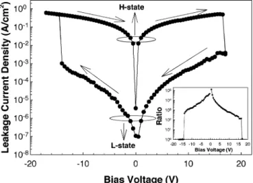
Fig. 1. Leakage current density versus bias voltage for Crdoped SrZrO -based MIM device. The inset shows the variation of the resistance ratio with the bias voltage.
II. EXPERIMENTAL
A 200-nm SiO layer was thermally grown on Si substrate in a furnace to prevent the leakage current from the Si sub-strate. A 50-nm SrTiO buffer layer and then a 60-nm LaNiO (LNO) bottom electrode film were deposited by radio frequency (RF) magnetron sputter on the SiO –Si substrate. Subsequently, a 90-nm 0.2% Cr-doped SrZrO (SZO) film was deposited at 450 C by RF magnetron sputter on LNO film as an insulator layer. The SZO film exhibits the (100), (110), and (200) peaks based on X-ray diffraction pattern (not shown here), indicating that it is polycrystalline structure. Finally, a 500-nm-thick Al film was deposited by thermal evaporation on the Cr-doped SZO films as a patterned top electrode of area cm to perform the electrical measurement with Agilent 4155C and 81 110A.
III. RESULTS ANDDISCUSSION
Fig. 1 shows the leakage current density versus bias voltage for the 0.2% Cr-doped SZO-based MIM device. The repro-ducible sequence of leakage current density can be traced from an increase of leakage current density for the high leakage (H) state with increasing bias voltage in the positive direction. At 15 V, the leakage current density rapidly decreased from H to low leakage (L) state. The leakage current density of the L-state increased with increasing bias voltage in the negative direction and rapidly increased from L to H state at 15 V. The switching voltage should relate to the crystallinity of the resistive film.
LIU et al.: BISTABLE RESISTIVE SWITCHING OF A SPUTTER-DEPOSITED Cr-DOPED SrZrO MEMORY FILM 353
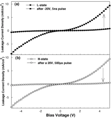
Fig. 4. (a) Leakage current density versus bias voltage for low leakage state and (b) for high leakage state after adding the voltage pulse indicated.
sweep would change the state to the other state. The resistance change driven by the voltage pulses had the same polarity direction with that driven by the bias voltages. We have made the same fitting as Fig. 2 using the data in Fig. 4 (not shown here). It is indicated that the conduction mechanism of L-state is dominated by Frenkel–Poole emission. Furthermore, it was found that the conduction mechanism of H-state is related to Frenkel–Poole emission under low bias voltage while under high bias voltage, the conduction of H-state is still governed by ohmic mechanism. This phenomenon may be attributed to that the pulse operation has smaller transition time than the dc voltage sweep. The transition time for the switching of the H- to
the state was five orders of magnitude longer than that of L-to H-state, implying that the transition from L- L-to H-state was easier than from H- to L-state. Therefore, the transition from H- to L-state is the restricted part for the reversible switching by voltage pulse operation.
IV. CONCLUSION
Cr-doped SZO films were deposited by RF magnetron sputter to fabricate the MIM device under investigation. This device with the properties of reversible switching, nondestructive readout, and a long memory time is suitable for nonvolatile memory application. The conduction mechanisms corre-sponding to H- and L-states were investigated to provide some explanations for resistive transition. The resistance transition could also be driven by voltage pulses. The transition time of H- to L-state was five orders of magnitude longer than that of L- to H-state.
REFERENCES
[1] M. S. Tsai, S. C. Sun, and T. Y. Tseng, “Effect of bottom electrode mate-rials and the electrical and reliability characteristics of (Ba, Sr) TiO ca-pacitors,” IEEE Trans. Electron Devices, vol. 46, no. 12, pp. 1829–1838, Dec. 1999.
[2] C. J. Haung, C. Y. Chang, and T. Y. Tseng, “Bolometric response of superconducting YBa Cu O microbridges,” J. Appl. Phys., vol. 72, pp. 5786–5791, 1992.
[3] C. Y. Liu, H. T. Lue, and T. Y. Tseng, “Effects of nitridation of silicon and repeated spike heating on the electrical properties of SrTiO gate dielectrics,” Appl. Phys. Lett., vol. 81, pp. 4416–4418, 2002.
[4] A. Beck, J. G. Bednorz, C. Gerber, C. Rossel, and D. Widmer, “Repro-ducible switching effect in thin oxide films for memory applications,”
Appl. Phys. Lett., vol. 77, pp. 139–141, 2000.
[5] Y. Watanabe, J. G. Bednorz, A. Bietsch, C. Gerber, D. Widmer, A. Beck, and S. J. Wind, “Current-driven insulator-conductor transition and nonvolatile memory in chromium-doped SrTiO single crystals,”
Appl. Phys. Lett., vol. 78, pp. 3738–3740, 2001.
[6] C. Rossel, G. I. Meijer, D. Bremauid, and D. Widmer, “Electrical cur-rent distribution across a metal-insulator-metal structure during bistable switching,” J. Appl. Phys., vol. 90, pp. 2892–2898, 2001.
[7] S. M. Sze, Physics of Semiconductor Device, 2nd ed. New York: Wiley, 1981.