國 立 交 通 大 學
電子工程學系 電子研究所碩士班
碩
士
論
文
銅製程中考量耦合電容與電鍍之無意義金屬擺放
用以改善平整度
Coupling Capacitance and ECP-Aware Dummy Metal Fill
for Layout Uniformity in Cu Process
研 究 生:柯宇倫
指導教授:陳宏明
銅製程中考量耦合電容與電鍍之無意義金屬擺放
用以改善平整度
Coupling Capacitance and ECP-Aware Dummy Metal Fill
for Layout Uniformity in Cu Process
研究生: 柯宇倫
Student : Yu-Lun Co
指導教授: 陳宏明 Advisor : Hung-Ming Chen
國 立 交 通 大 學
電子工程學系 電子研究所碩士班
碩士論文
A Thesis
Submitted to Department of Electronics Engineering & Institute of Electronics College of Electrical Engineering and Computer Science
National Chiao Tung University in Partial Fulfillment of Requirements
for the Degree of Master of Science
in
Electronics Engineering December 2007
Hsinchu, Taiwan, Republic of China
i
銅製程中考量耦合電容與電鍍之無意義金屬擺放用以改善平整度
研究生:柯宇倫 指導教授:陳宏明
國立交通大學
電子工程學系 電子研究所碩士班
摘要
晶片在新一代製程中,隨著特徵尺寸的縮小,在製造困難度及可靠度上相對遇到 的困難也越來越多。這種情況下,使得必須要有更良好的晶片表面平整度才能改善晶 片的性能和參數良率。普遍用來降低晶片表面地形變化的方法是在佈局上較空曠的區 域中填入一些無意義的金屬,然而,這些填入的金屬會增加導線之間的電容因而造成 延遲和耦合/串擾等雜訊問題。 在這篇論文中,我們提出了一個演算法特別去考慮到一些佈局上會影響電镀表面 的參數來做無意義金屬的填入,同時我們使用一個貪婪演算法來放置這些金屬,使得 額外增加的耦合電容能達到最小。在實驗結果方面,我們與傳統上以佈局密度為主的 演算法做比較,我們的方法在電鍍後厚度差和等效密度差上都能有顯著的改善,這表 示對晶片表面的地形平整度能有明顯的改善。而且,我們放置無意義金屬的方法也能 有效降低額外增加的耦合電容。ii
Coupling Capacitance and ECP-Aware Dummy Metal Fill for Layout
Uniformity in Cu Process
Student : Yu-Lun Co Advisor : Hung-Ming Chen
Department of Electronics Engineering
& Institute of Electronics
National Chiao Tung University
Abstract
With feature sizes on chips shrinking at new process node, the difficulty in manufacturability and reliability of chips is increasing. It has necessitated better planarization of chip surface topography to improve both functional and parametric yield. The common solution to minimize topography variation is to insert dummy metals in empty spaces in the layout. However, these dummy metals will increase the capacitances between wires and then invoke delay and coupling/crosstalk noise problems.
In this thesis, we propose an algorithm to consider especially the key layout parameters that affect the post-ECP (electroplating) topography and we use a greedy method to place the dummy metals with minimal additional coupling capacitances. Compared with a traditional density-based algorithm, the experimental result shows that our method has significant improvement on both post-ECP thickness variation and effective density variation which means the significant improvement in planarization of chip surface topography. Furthermore, our placing method of dummy metals can reduce the additional coupling capacitances efficiently.
v
誌謝
兩年碩士生活隨著論文結束而終止,首先要感謝的是指導教授陳宏明老師, 繁忙之際仍耐心地給予我啟發和指導,以及進實驗室以來安排的一些訓練,都讓 我獲益良多。感謝兩位口試委員,鄭儀侃博士和李育民教授研究方法上的悉心指 教及寶貴的意見,使得我的論文能夠更加地完整。 另外,也要感謝實驗室所有的成員,兩年來大家互相討論和鼓勵,你們的陪 伴使得研究生活更加的豐富而且有趣。當然還要感謝家人對我的支持與體諒,你 們的支持才是在研究路上支持我前進最大的動力。 要感謝的人太多了,即使只是一場演講上給予我的啟發,或是朋友間一句鼓 勵的話,對我來說都別具意義。最後由衷感謝所有幫助關懷過我的人。 柯宇倫 民國九十六年十二月 於新竹Coupling Capacitance and ECP-Aware Dummy
Metal Fill for Layout Uniformity in Cu Process
Student: Yu-Lun Co
Adviser: Prof. Hung-Ming Chen
For the Degree of
Master of Science
Department of Electronics Engineering
National Chiao Tung University
Contents
1 Introduction 1 2 Preliminaries 3
2.1 ECP topography model . . . 3
2.2 2D low-pass filter CMP model . . . 7
2.3 Different types of dummies . . . 8
2.4 Problem formulation . . . 9
3 Proposed algorithm 12 3.1 Greedy heuristics for layout density and perimeter assignment . . . . 13
3.2 Dummy fill placement with minimal coupling capacitances . . . 16 4 Experimental result 19 5 Conclusion 22 Bibliography 22
List of Figures
2.1 A typical topography after ECP process [7] . . . 4
2.2 An arbitrary layout in window with size DxD . . . 5
2.3 Three typical ECP topography cases [7] . . . 5
2.4 Case selection of ECP topography . . . 7
2.5 The weighting filter function used to transfer local pattern density to effective density. . . 8
2.6 Possible dummy shapes: (a) square, (b) rectangular, (c) parallel line, and (d) orthogonal dummy [4]. . . 9
2.7 Total capacitance increments with different types of metal dummy [4]. 9 2.8 Profile after ECP and CMP [10]. . . 10
3.1 The flow chart of dummy fill insertion algorithm. . . 12
3.2 (a) empty rectangles within tile (b) fill-able regions . . . 13
3.3 Capacitance increment : (a) dummy at track 0 (b) dummy at other track . . . 17
List of Tables
4.1 The experimental results of proposed algorithm . . . 19 4.2 The comparison of dummies placing methods . . . 20
Chapter 1
Introduction
Continued aggressive scaling down of VLSI feature size has necessitated better planarization of chip surface topography to improve both functional and parametric yield. Non-planar chip surface can eat into the depth of focus (DOF) budget and also produce resistance and capacitance variations which can adversely impact chip timing. The commonly approach to improve the planarity of chip surface is to insert electrically inactive features (also known as metal fills or dummies) in the empty spaces in the layout to reduce the variations in key layout characteristics.
In the past, the primary objective of metal filling mostly focus on even layout density [2] [12]. This can be attributed to the fact that most metal filling solutions were originally developed to obtain better planarization after inter-layer dielectric (ILD) chemical mechanical polishing (CMP) in Al metallization process. Previous work by Ouma [8] shows that the ILD thickness is primarily a function of the un-derlying density. Hence, it sufficed to have a metal filling algorithm that sought to reduce the density differences between the different regions of the layout to attain smaller final thickness range. However, in Cu metallization process, there are vari-ous layout characteristics (besides density) which will affect planarity of chip surface and should be considered in metal fill algorithm.
Electroplating (ECP) and CMP are two key steps in the Cu fabrication process. The variations in the post-ECP topography are propagated through the CMP steps, thereby affecting the final surface topography. In our approach, we apply the ECP model of [7] to get the post-ECP thickness from layout characteristics and evaluate the effective density to indicate the final planarity of chip surface after CMP process. As we insert dummies to improve the chip planarity, the interconnection capac-itances will increase and then invoke delay and coupling/crosstalk noise problems. Therefore, another objective is to decide the positions of dummies in the empty spaces with minimal coupling capacitances. The computation of coupling capaci-tance increment refers to the capacicapaci-tance model for intra-layer dummies in [4] [1] [3]. In this thesis, we begin with the descriptions of ECP and CMP models and briefly explain how the two processes affect the chip surface in Chapter 2. In Chapter 3, we proposed an algorithm to improve the planarity and reduce the capacitive incre-ment due to dummy insertion. We show the experiincre-mental results of the algorithm in Chapter 4, and conclude in Chapter 5.
Chapter 2
Preliminaries
In this chapter, we introduce two important models that are applied in our al-gorithm. The first one is the electroplating (ECP) topography model, which is developed based on the additive nature of the physics of the ECP process [7], and it can predict the post-ECP topography by the strong dependency of post-ECP thickness and layout characteristic. The second one is the 2D low-pass filter CMP model, which is used to determine the effective density of each panel by weighting the influence of nearby panel density.
2.1
ECP topography model
During the copper(Cu) Damascene process, trenches and holes are first etched in the oxide material. An ECP process is applied to deposit the copper onto the whole wafer filling up the trenches. It is followed by a CMP process in which excess overflowing copper is removed from the oxide surface leaving copper in the intended trenches and holes. And the interconnect wires and vias are formed.
Figure 2.1 shows an example of a typical topography after ECP. Post-ECP to-pography can be described by two parameters: step-height and array-height. The
Figure 2.1: A typical topography after ECP process [7]
array height H is defined as the thickness of Cu above the oxide after deposition; the step height S is defined as the difference of Cu height between the Cu above the oxide and the Cu above the trench in the oxide. We can observe that the Cu thickness after ECP process strongly depends on wires attributes of the region.
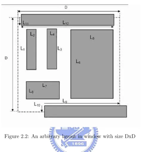
Before we further discuss the ECP topography model, we should give the defini-tions of several layout parameters first. They are the perimeter sum L, the feature density ρ, shrunk density ρs , expanded density ρe. For an arbitrary layout in
window with size D×D shown in Figure 2.2,
L = 2(L1 + L2 + L3 + L4 + L5 + L6 + L7 + L8) + L9 + L10 + 2L11 + L12 ρ = the area of all the layout objects (or feature trenches)
divided by the total area of the design
ρs= the feature density after shrinking all the
layout features by an amount of δs
ρe= the feature density after expanding all the
Figure 2.2: An arbitrary layout in window with size DxD
There are primarily three different topographies that result after an ECP process. For simplicity of the presentation, Figure 2.3 shows these three topographies for a single wire only. However, the following discussions are applicable to multi-wires as well.
Figure 2.3: Three typical ECP topography cases [7]
for each case: Case 1 (conformal-fill): H = H0 1 − ρ 1 − ρs (2.1) S = H0 1 − ρ (1 − ρs)ρs + T ρ ρs − H0 TeL D2ρ s −H0 ρs (2.2) Case 2 (super-fill): H = H0 (2.3) S = T ρ ρe − H0 TeL D2ρ e (2.4) Case 3 (over-fill): H = H0+ H0 TeL D2 − T ρ (2.5) S = 0 (2.6)
where H0 is the field copper thickness, T is the feature trench depth.
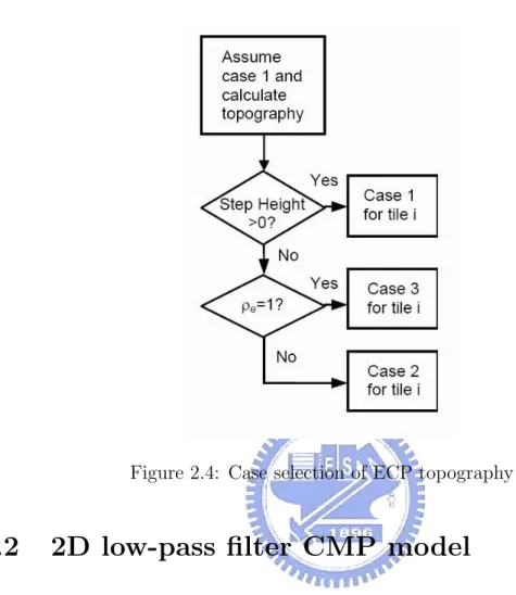
Because of the evolution process of topography described in [2], the case selection must follow the flow chart shown in Figure 2.4.
As this model is developed, we can get post-ECP topography by evaluating the step height and array height. We can reduce post-ECP height difference in dummy insertion algorithm to lower the influence on sequential CMP process, which will be discussed in Chapter 3.
Figure 2.4: Case selection of ECP topography
2.2
2D low-pass filter CMP model
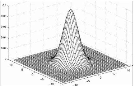
After Cu deposited onto the wafer, excess overflowing Cu is removed from the oxide surface in CMP process. A detailed CMP process models, which take process parameters such as slurry contents, down pressure, pad material and pad speed into consideration, are usually complicated. However, an abstract-level model may be simple since the CMP process that is designed to polish uneven surfaces is analogous to a low-pass ”filter”. A 2-D low-pass-filter CMP model is found to be both efficient and easy to calibrate [9][13].
As we know, for more uniform ECP profiles, there is a dependence between the final thickness and the density [6]. The thickness in such cases is inversely proportional to the effective density, which is a function of the local density. After the layout is discretized to rectangle panels, the effective density at the center of
Figure 2.5: The weighting filter function used to transfer local pattern density to effective density.
panel (i,j) is a 2-D convolution of the local pattern density with the filter function. The effective density ρef f (i,j) can be calculated using [11]:
ρef f (i,j) = IFFT[ FFT[ρ(i,j)] ∗ FFT[f(i,j)] ] (2.7)
where ρ(i,j) is local pattern density, and f(i,j) is the weighting filter function
shown in Figure 2.5.
2.3
Different types of dummies
For the dummy metal fill problem, there are floating dummies and grounded dummies. Before we talk about our algorithm, we have to mention that the type we use is floating dummies while some of prior works choose grounded stripe metals as their dummies. Grounded dummies are not desirable due to both their higher impact on capacitance and also routing difficulties in current technology nodes, al-though they are more stable and easy to extract.
Figure 2.6: Possible dummy shapes: (a) square, (b) rectangular, (c) parallel line, and (d) orthogonal dummy [4].
Figure 2.7: Total capacitance increments with different types of metal dummy [4].
In addition, different shapes of dummies will cause different capacitance incre-ment. Figure 2.6 present the four possible types of dummy shapes. Figure 2.7 shows the square, floating dummy has least capacitance increment and consequently was used for insertion in our approach [5][4].
2.4
Problem formulation
Most prior model-based solutions use an ILD thickness model to guide the metal filling process. The ILD thickness model states the dielectric thickness at a location
Figure 2.8: Profile after ECP and CMP [10].
is proportional to the convolution of the metal density and a suitable weighting function which considers the deformation of the polishing pad during CMP. All of these model-based solutions focus primarily on metal density and does not consider the impact of ECP. However, there are experiments show that different regions with the same density have different final thickness values after Cu ECP and CMP [10]. Therefore, it can be concluded that it is not sufficient to consider only density during metal filling for copper processes.
Figure 2.8 shows that the variations in the ECP topography are propagated through the CMP steps, thereby affecting the final surface topography. For this reason, one of our objectives is to reduce the post-ECP thickness range (i.e. height difference between highest and lowest point) by changing layout characteristics with dummies.
As long as the post-ECP topography is smooth, there is dependence between the final thickness and the effective density. Our another objective is inserting dummies
to reduce effective density range, at the same time, without increasing post-ECP thickness range.
Although metal filling is an effective method to improve chip planarity, it draws some drawbacks. The more dummies we inserted, the more capacitances would be induced. These additional capacitances will result delay or crosstalk problems. Ac-cordingly, another consideration is to reduce the additional capacitances by put the dummies we inserted into suitable place between empty spaces of layout.
Chapter 3
Proposed algorithm
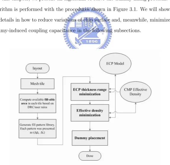
In this chapter, we present an algorithm to solve the dummy filling problem. The algorithm is performed with the procedures shown in Figure 3.1. We will show the the details in how to reduce variations of chip surface and, meanwhile, minimize the dummy-induced coupling capacitance in the following subsections.
3.1
Greedy heuristics for layout density and
perime-ter assignment
The key layout parameters that are considered in this step are density and perimeter since ECP thickness profile primarily depends on both parameters and the effective density depends only on density. The manipulation of adjusting these parameters between tiles can improve chip surface planarity.
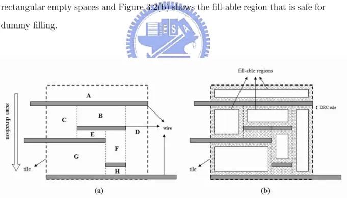
We start with meshing the layout of design into non-overlapping tiles, and then slicing the layout to get empty spaces for dummy insertion. Figure 3.2(a) shows the rectangular empty spaces and Figure 3.2(b) shows the fill-able region that is safe for dummy filling.
Figure 3.2: (a) empty rectangles within tile (b) fill-able regions
Parameter assignment has two main steps. In the first step, our objective is to reduce the post-ECP height difference. And we minimize the effective density range without increasing post-ECP height difference in the second step. Throughout both steps, we change layout parameters of each tile by appending a combination of
den-sity and perimeter, which is chosen from the established fill pattern library. As long as the parameters are assigned, we apply the ECP and CMP model to check that the topography is convergent or not. Following processes are the greedy heuristics for parameters assignment:
Greedy Heuristics for Density and Perimeter Assignment : 1. Layout Preparation :
(a) Mesh the layout into non-overlapping tiles. Denote the ith tile as Ti.
(b) Determine the fill-able areas in each tile based on DRC rules. The fill-able density of the tile Ti is denoted as dFi .
(c) Generate a fill pattern library which includes many (density, perimeter) com-binations that can be assigned to tiles. The set of comcom-binations is denoted as CS.
2. Reduce ECP Thickness Range :
(a) Intra-tiles ECP thickness range minimization (b) Inter-tiles ECP thickness range minimization
3. Minimize Effective Density Range :
(a) Restricted effective density range minimization
The detail of the minimization algorithms will be provided below. After the heuristics are performed, we get the target density and perimeter of each tile that can make the chip more smooth. With these parameters, we know how many and how large dummies should be inserted in each tile. However, the positions of the dummies are not really decided. Following section we will have the discussions about this part.
Intra-tiles ECP thickness range minimization algorithm For each tile Ti
Determine ECP case by ECP model. If Ti is not over-fill case
For each c = (dc
k, Lck) ∈ CS and dck < dFi .
Let dc
k and Lck add to the tile’s parameters temporarily.
If the tile is over-fill case.
Break
Else
Restore the tile’s parameter .
Update the fill-able density. dF
i = dFi − dck.
Inter-tiles ECP thickness range minimization algorithm
1. Determine the ECP thickness Hi of all tiles and denote maximum as Hmax.
2. Compute priority of each tile as a function of Hmax− Hi. And sort the tiles
according to the priority function. 3. For all tiles in sequence
Hdif f = ∞
For each c = (dc
k, Lck) ∈ CS and dck< dFi .
Let dc
k and Lck add to the tile’s parameters temporarily.
Compute Hi by ECP model.
If Hmax− Hi< Hdif f
copt= c
Hdif f = Hmax− Hi
Break Else
Restore the tile’s original parameters.
Restricted effective density range minimization algorithm
1. Determine the effective density ρi of all tiles and denote maximum as ρmax.
2. Unlocked each tile Ti and compute its priority as a function of ρmax − ρi.
And sort the tiles according to the priority function. 3. For all tiles in sequence
ρdif f = ρmax− ρmin
For each c = (dc
k, Lck) ∈ CS and dck< dFi .
Let dc
k and Lck add to the tile’s parameters temporarily.
Compute Hi and ρi of each tile by ECP and CMP model.
If ρmax− ρmin< ρdif f, and ECP thickness range does not increase If for each neighbor tile in CMP radius, its ρ ≤ ρmax
copt = c
ρdif f = ρmax− ρi
Break Else
Restore the tile’s original parameters.
Assign copt to the tile and update the fill-able density. dFi = dFi − d copt
k .
3.2
Dummy fill placement with minimal coupling
capacitances
Dummy fill insertion is an effective and widely-used method to improve chip planarity. However, these dummy metals will increase coupling capacitances and bring some problems. Placing the dummies to suitable positions in the empty spaces may reduce the capacitive increments. The coupling capacitance introduced by dummies can be evaluated by the closed-form equation [3] as shown below:
C = C0
l dα
where C0 is the coupling parameter, α is an experimentally estimated constant, l
is the coupling length, and d is the distance between two segments. C0 and α are
technology related constants, α ∈ (1, 2) for the current technology.
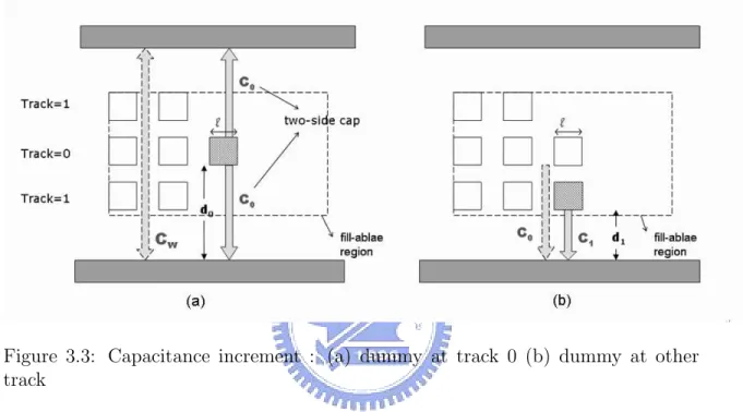
Figure 3.3: Capacitance increment : (a) dummy at track 0 (b) dummy at other track
As shown in Figure 3.3, when we select a dummy at track 0, the dummy will introduce new coupling capacitances for both side. When we select a dummy at other tracks, it will introduce new coupling capacitances on one side and block some old coupling capacitance. Assume the dummies at higher tracks can be inserted only if dummies at lower track are inserted, then, the increase of the coupling capacitance for the dummy at track i can be formulated as following:
Additional cap cost = (1 Ci + 1 Ci) −1− C w · l if i=0, 1 2[(C1i + 1 Ci) −1− ( 1 Ci−1 + 1 Ci−1) −1] otherwise. (3.1)
where l is dummy width, Cw is cap per unit before inserting any dummies, and Ci
In the previous parameter assignment step, we get target density ρ and perimeter
L of each tile. Since we choose square dummies to be inserted, we can easily compute
the dummies numbers N and their width w of each tile from its target density and target perimeter. Following equations are the relations of these parameters:
Lf ill = N · 4w (3.2)
ρf ill = N ·
w2
T ileW idth2 (3.3)
After we get dummies amount N, dummy width w, and the cap cost of each possible position, the minimization of capacitances within a tile is just choosing lowest-cost positions until N dummies are inserted. Notice that the selection of possible dummy position should keep the order from lower tracks to higher tracks.
Chapter 4
Experimental result
Here, we present the experimental result for two chips to validate the proposed algorithm. The first one (D1) is 3.4×3.4mm2 for 0.13µm 1P8M process and the
sec-ond one (D2) is 3.9 × 3.9mm2 for 90nm 1P9M process. For both designs, we choose
an 1 × 1mm2 dissection and mesh it into 20 × 20 tiles to perform the algorithm.
In Table 4.1, the ρef f range of original chip means the peak-to-peak value of
effective density between tiles. We first compute local density from layout patterns, and then get the effective density by the low-pass filter CMP model. The layout patterns before dummy filling are only composed of routing wires. When the dum-mies are inserted, the density of dumdum-mies will be counted in.
Table 4.1: The experimental results of proposed algorithm Original chip After our approach
Test Avg. ρef f Post-ECP Avg. ρef f Post-ECP
case ρef f range thickness range ρef f range thickness range
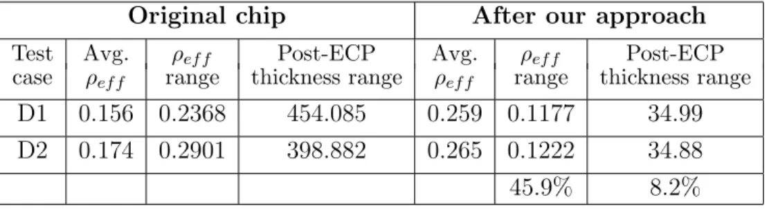
D1 0.156 0.2368 454.085 0.259 0.1177 34.99 D2 0.174 0.2901 398.882 0.265 0.1222 34.88 45.9% 8.2%
As we mentioned before, The effective density is the key indicator of final thick-ness only if the ECP topography is more smooth. Therefore, the changes of post-ECP thickness range is important and is also shown in the table. We can observe that the post-ECP thickness range becomes 8.2% of original chip and effective den-sity range becomes 45.9% after the proposed algorithm. It means that the ECP topography is really smooth, and therefore we can say the final thickness range is reduced to about 45.9% of original thickness range after our algorithm.
After the numbers of fills are assigned to tiles, the methods of placing fills will affect coupling capacitances. Traditional dummy fill insertion are based on even effective density. Thus, for each tile, the fills are distributed to fill-able regions by their area to get even density on tile scale. We compare our method with density driven method in Table 4.2. The additional capacitance is the increment of the capacitances from the same layer after the dummy fills insertion is applied.
Table 4.2: The comparison of dummies placing methods Additional capacitance
Test case density driven method our method improvement
D1 4528 1804 60.2% D2 3877 1299 66.5%
In the density driven method, each tile Ti has many non-overlapping fill-able
regions Rij, where
P
Rij = Fi(total fill-able area). For each Rij, the dummies
number is equal to {target dummies numbers×Rij/Fi} [10]. Therefore, the dummies
are evenly distributed in a tile. And then dummies are put into Rij from center track
has less additional capacitances than the density-driven method, thereby having less coupling/crosstalk noise problems.
Chapter 5
Conclusion
In this thesis, a metal filling algorithm that is based on the physical models of the copper damascene process was presented. Key predictors of final thickness range that can be efficiently computed were identified and used to drive metal filling. Experimental results indicate that the proposed method can significantly reduce the post-ECP thickness range and effective density range after metal filling. Also, we take the capacitances into consideration, for which will definitely increase after metal filling and cause unwanted effect. The proposed method can significantly reduce the additional coupling capacitances when compared to the density-driven approach.
Bibliography
[1] Y. Chen, P. Gupta, and A. Kahng. “Performance-Impact Limited Area Fill Synthesis”. In Proc. ACM/IEEE Design Automation Conf., pages 22–27. June 2003.
[2] Y. Chen, A. Kahng, G. Robins, and A. Zelikovsky. “Dummy Fill Synthesis for Uniform Layout Density”. In IEEE Trans. on Computer-Aided Design. January 2002.
[3] L. Deng, D.-F. Wang, K.-Y. Chao, and H. Xiang. “Coupling-Aware Mixed Dummy Metal Insertion for Lithography”. In Proceedings of SPIE 6521. 2007. [4] Y. Kima, D. Petranovic, and D. Sylvestera. “Simple and Accurate Models for
Capacitance Increment due to Metal Fill Insertion”. In ASPDAC. 2007. [5] K.-H. Lee, J.-K. Park, and Y.-N. Yoon. “Analyzing the effects of floating
dummy-fills: from feature scaleanalysis to full-chip RC extraction”. In Electron
Devices Meeting, 2001. IEDM Technical Digest. International, pages 31.3.1–
31.3.4. 2001.
[6] J. Luo and D. A. Dornfeld. “Integrated Modeling of Chemical Mechanical Planarization for Sub-Micron IC Fabrication: from Particle Scale to Feature, Die and Wafer Scales”. In Springer-Verlag. Berlin, Germany, 2004.
[7] J. Luo, Q. Su, C. Chiang, and J. Kawa. “A Layout Dependent Full-Chip Copper Electroplating Topography Model”. In Proceedings IEEE/ACM International
Conference on Computer-Aided Design. 2005.
[8] D. Ouma. “Modeling of Chemical Mechanical Polishing for Dielectric Planariza-tion”. In Ph. D. Dissertation, Dept. of EECS, MIT. Cambridge, MA, USA, 1998.
[9] D. Ouma, D. Boning, J. Chung, G. Shinn, L. Olsen, and J. Clark. “An in-tegrated characterization and modeling methodology for CMP dielectric pla-narization”. In Proc. Int. Interconnect Technology Conf., pages 67–69. San Francisco, CA, June 1998.
[10] S. Sinha, J. Luo, and C. Chiang. “Model Based Layout Pattern Dependent Metal Filling Algorithm for Improved Chip Surface Uniformity in the Copper Process”. In ASP-DAC. 2007.
[11] R. Tian, D. Wong, and R. Boone. “Model-based dummy feature placement for oxide chemical-mechanical polishing manufacturability”. In IEEE Trans. CAD, volume 20, pages 902–910. July 2001.
[12] X. Wang, C. C. Chiang, J. Kawa, and Q. Su. “A min-variance iterative method for fast smart dummy feature density assignment in chemical-mechanical pol-ishing ”. In ISQED 2005, pages 258 – 263.
[13] T. Yu, S. Cheda, J. Ko, M. Roberton, A. Dengi, and E. Travis. “A two dimen-sional low pass filter model for die-level topography variation resulting from chemical mechanical polishing of ILD films”. In Proc. IEDM. Washington, DC, Dec. 1999.
作者簡歷
柯宇倫,民國七十二年三月出生於台北縣。民國九十四年六月畢業於國立中 正大學電機系,並於同年九月進入國立交通大學電子研究所就讀,從事 VLSI 實 體設計方面相關研究。民國九十六年十二月取得碩士學位,碩士論文題目為『銅
![Figure 2.1: A typical topography after ECP process [7]](https://thumb-ap.123doks.com/thumbv2/9libinfo/8747374.205225/13.918.212.679.155.400/figure-typical-topography-ecp-process.webp)
![Figure 2.7: Total capacitance increments with different types of metal dummy [4].](https://thumb-ap.123doks.com/thumbv2/9libinfo/8747374.205225/18.918.235.660.446.677/figure-total-capacitance-increments-different-types-metal-dummy.webp)
![Figure 2.8: Profile after ECP and CMP [10].](https://thumb-ap.123doks.com/thumbv2/9libinfo/8747374.205225/19.918.192.704.156.454/figure-profile-after-ecp-and-cmp.webp)