國
立
交
通
大
學
電子工程學系電子研究所碩士班
碩 士 論 文
釩摻雜鋯酸鍶記憶體薄膜之
雙穩態電阻轉換特性
Bistable Resistive Switching Properties of
V
2O
5-doped SrZrO
3Memory Films
研 究 生:杜丙章
指導教授:曾俊元
釩摻雜鋯酸鍶記憶體薄膜之
雙穩態電阻轉換特性
Bistable Resistive Switching Properties of
V
2O
5-doped SrZrO
3Memory Films
研 究 生: 杜丙章
Student: Bing-Chung Tu
指導教授:曾俊元
Advisor: Tseung-Yuen Tseng
國 立 交 通 大 學
電子工程學系電子研究所碩士班
碩 士 論 文
A Thesis
Submitted to Department of Electronics Engineering & Institute of Electronics
College of Electrical and Computer Engineering
National Chiao-Tung University
in Partial Fulfillment of the Requirements
for the Degree of Master
in
Electronic Engineering
June 2006
Hsinchu, Taiwan, Republic of China
釩摻雜鋯酸鍶記憶體薄膜之
雙穩態電阻轉換特性
學生:杜丙章 指導教授:曾俊元 教授 國立交通大學電子工程學系電子研究所碩士班摘要
近來,由各種材料所研製的各類新式非揮發性記憶受到廣泛的注意。其中, 電阻式記憶體由於具有雙穩態電阻值特性,可在同一偏壓下表現出兩種不同電阻 值之特性,並且具有高寫入及讀取速度,非破壞性讀取,結構簡單(金屬—絕緣 體—金屬之結構)的優點,將有助於達到高密度積體整合,低功率損失的目的。 因此電阻式記憶體儼然成為下一世代非揮發性記憶體之候選人。 在本篇論文中,我們使用釩摻雜的鋯酸鍶(鈣鈦礦結構材料)來製作電阻式 記憶體。首先,我們將介紹鈣鈦礦結構及基本的電流-電壓雙穩態電阻值轉換特 徵。在實驗的部分,我們使用濺鍍法製造不同濃度釩摻雜的鋯酸鍶記憶體薄膜, 並以鎳酸鑭作為底電極,鋁作為上電極來形成金屬—絕緣體—金屬的結構。然後 將其物理及電學特性將於第三章報告。最後,我們也將歸納出元件的電流傳導機 制,並探討不同濃度釩摻雜的影響對元件的影響。Bistable Conductivity Switching Memory Devices Using
Perovskite Oxide Thin Films By Sputtering Method
Student: Bing-Chung Tu Advisor: Tseung-Yuen Tseng
Department of Electronics Engineering and Institute of Electronics
National Chiao Tung University
Abstract
Recently, many kinds of new nonvolatile memory manufactured from different materials have attracted a large attention. The resistance random access memory (RRAM) has bistable resistive switching character which can exhibit two states of different resistance at the same applied voltage. Besides, high speed of writing and access, nondestructive readout, simple device structure (Metal-Insulator-Metal structure) that is useful to promote the high density of integration, lower power consumption. Accordingly, RRAM has been proposed to be one candidate of next generation nonvolatile memory.
In this thesis, the RRAM device was manufactured based on perovskite structure— V-doped SrZrO3. First, we would introduce the perovskite structure and
fundamental Current-Voltage characters of the bistable resistive switching behavior. In experimental part, the vanadium (V)-doped SrZrO3 memory film with different
dopant concentration deposited by sputtering method was sandwiched between bottom electrode (LaNiO3) and top electrode (Aluminum) to form MIM structure. Its
physical and electrical properties would be reported in chapter 3. Finally, we would decline the conduction mechanism of the device and discuss the influence of the various dopant concentrations.
致 謝
首先要感謝我的指導教授曾俊元老師。老師在實驗跟研究
上追根究底、實事求是的精神,對我未來的生活及處世上都
有啟發,而且在實驗方面提供豐富的資源,讓我能順利完成
論文。
此外,也要感謝國家豪微米實驗室,清大貴重儀器中心等
單位,提供良好的研究環境,在此也一併致謝!
另外,我也要感謝林群傑和林志洋兩位博班學長,無論在
實驗或課業上的協助與建議,使我獲益良多。還有感謝李佳
穎學姐、周秀玉學姐、賴俊宏學長、林昭正學長、張家瑋同
學、柳星舟同學、蔡信賢同學,以及尤俊勝、吳重毅、吳鎮
宇、黃俊興、簡士傑、余崧蒔、陳冠仲、姚承佑學弟們,陪
我一起度過這兩年美好的研究所歲月。
最後,要感謝我的家人,全力支持我念研究所,無論是在
精神上或是物質上的協助及鼓舞,讓我無後顧之憂全力專心
在課業上,我才能順利完成學業,謝謝你們!
Contents
Abstract (in Chinese)...i
Abstract (in English)...ii
Acknowledgement ...iii
Contents ...iv
Table Captions ...vi
Figure Captions ...vi
CHAPTER 1 Introduction
1.1 Introduction to nonvolatile memory ………... 1
1.2 Introduction to Resistive Random Access Memory (RRAM) . 1
1.2.1 The Structure and Operation Method of RRAM ……... 2
1.2.2 Material Groups of RRAM ……… 2
1.3 Introduction to Perovskite Materials ……….. 3
1.4 Resistive Switching Properties of doped SrZrO
3films ….…. 4
CHAPTER 2 Experiment details
2.1 Experiment Process Flow ………... 6
2.2 RF Magnetron Sputter System ………. 7
2.2.1 Vacuum system ……….. 7
2.2.2 Pressure system ……… 7
2.2.3 Temperature controlling system ……… 7
2.2.4 Gas flow controlling system ………... 8
2.2.6
Cooling
system
……….. 8
2.3 Preparation ………... 8
2.3.1 Sputtering Targets ……… 9
2.3.2 Thin films deposition ……….. 10
2.4 Measurements and Analysis ……….. 12
2.4.1 X-Ray Diffraction (XRD) ………. 12
2.4.2 Scanning Electron Microscope (SEM) ………... 12
2.4.3 Current-Voltage (I-V) Measurements ……….. 13
CHAPTER 3 Results and Discussion
3.1 Physical Properties of LNO Bottom Electrodes and Doped SZO
Films ……… 15
3.2 Electrical Properties of SZO & 0.1% V-doped SZO Films … 17
3.3 Electrical properties of 0.2% V-doped SZO Films …………. 17
3.4 Electrical properties of 0.3% V-doped SZO Films …………. 20
3.5 Effect of Different Sputtering Temperature ……… 22
3.6 Effect of Different SZO Thickness ……… 23
TABLE CAPTIONS
Table 3-1 The recipes for the device fabricated with pure SZO and 0.1% V-doped SZO.
Table 3-2 The recipes for the device fabricated with 0.2% V-doped SZO and 0.3% V-doped SZO.
FIGURE CAPTIONS
Fig.1-1 RRAM consists of a transistor and a resistor. The transistor is fabricated in the front and the resistor in the back end.
Fig.1-2 Equivalent circuit of an array for the write operation of a given bit resistor.
Fig.1-3 Equivalent circuit of an array for the erase operation of a given bit resistor.
Fig.1-4 Basic structure of perovskite material
Fig.1-5 The phase of S21 of BST/HR-Si CPW transmission lines measured at zero gate bias after TRL calibration
Fig.2-1 The illustration of our experimental flow Fig.2-2 The preparation flow of our device Fig.2-3 The cross section of the MIM device Fig.2-4 The figure of the sputter system
Fig.2-5 The synthesis flow chart of LNO powder
Fig.2-6 The synthesis flow chart of doped SZO powder Fig.3-1 The SEM image of As-deposited LNO film
Fig.3-2 SEM image of LNO film annealed at 700℃ in O2 ambience for 1 min
Fig.3-3 The XRD patterns of LNO bottom electrodes
Fig.3-4 The XRD pattern of V-doped SZO films deposited at different temperatures
Fig.3-5 The SEM image of V-doped SZO film Fig.3-6 The IV curve of the pure SZO film
Fig.3-7 The IV curve of the 0.1% V-doped SZO film Fig.3-8 The IV curve of the 0.2% V-doped SZO film
Fig.3-9 The current fitting of the H-state for IV curve in the 4th cycle Fig.3-10 The current fitting of the L-state for IV curve in the 4th cycle Fig.3-11 The current fitting of the H-state for IV curve in the 14th cycle Fig.3-12 The current fitting of the L-state for IV curve in the 14th cycle
Fig.3-13 The endurance test of the 0.2% V-doped SZO film Fig.3-14 The current fitting of IV curve in the 1st cycle Fig.3-15 The current fitting of IV curve in the 10th cycle Fig.3-16 The current fitting of IV curve in the 100th cycle Fig.3-17 The uniformities of the 0.2% V-doped SZO film
Fig.3-18 IV curve measurement of the 0.3% V-doped SZO film Fig.3-19 The uniformities of the 0.3% V-doped SZO film
Fig.3-20 The current fitting of the H-state for IV curve in the 0.3% V-doped SZO film
Fig.3-21 The current fitting of the L-state for IV curve in the 0.3% V-doped SZO film
Fig.3-22 The current of the H-state and the L-state for IV curve in the 0.3% V-doped SZO film
Fig.3-23 The endurance test at 70℃ of the 0.3% V-doped SZO film Fig.3-24 The endurance test at 150℃ of the 0.3% V-doped SZO film
Fig.3-25 The current fitting of the current for IV curve in the 300th cycle in the 0.3% V-doped SZO film
Fig.3-26 The non-destructive readout test of the H-state at room temperature in the 0.2% V-doped SZO film
Fig.3-27 The non-destructive readout test of the L-state at room temperature in the 0.2% V-doped SZO film
Fig.3-28 The non-destructive readout test at room temperature in the 0.2% V-doped SZO film
Fig.3-29 The non-destructive readout test of the H-state at 85℃ in the 0.2% V-doped SZO film
Fig.3-30 The non-destructive readout test of the L-state at 85℃ in the 0.2% V-doped SZO film
Fig.3-31 The non-destructive readout test at 85℃in the 0.2% V-doped SZO film
Fig.3-32 The non-destructive readout test of the H-state at room temperature in the 0.3% V-doped SZO film
Fig.3-33 The non-destructive readout test of the L-state at room temperature in the 0.3% V-doped SZO film
Fig.3-34 The non-destructive readout test at room temperature in the 0.3% V-doped SZO film
Fig.3-35 The non-destructive readout test of the H-state at 85℃ in the 0.3% V-doped SZO film
V-doped SZO film
Fig.3-37 The non-destructive readout test at 85℃ in the 0.3% V-doped SZO film
Fig.3-38 The endurance test with the higher voltage (-5V) of the 0.3% V-doped SZO film
Fig.3-39 The retention test of the 0.3% V-doped SZO film
Fig.3-40 The IV curves of the 0.2% V-doped SZO films with different sputtering temperature.
Fig.3-41 The IV curves of the 0.2% V-doped SZO films with different sputtering temperature.
Chapter 1 Introduction
1.1 Introduction to Nonvolatile Memory (NVM)
Recently, many new memory materials have been proposed for next generation NVM application due to the popularity of portable equipments, such cell phone, digital camera, and MP3 player. The NVM should keep the stored data for a long time without any power supply. A perfect NVM should have the superior properties, including simple structure, low power consumption, high operation speed, low operation voltage, long retention time, high endurance, non-destructive readout, and small cell size [1]. However, flash memory, the mainstream of NVM nowadays, has many drawbacks in high operation, such as low operation speed, high operation voltage, poor endurance, and its congenital limit in size due to gate oxide thinning that causing poor retention.
1.2 Introduction to Resistive Random Access Memory (RRAM)
Lately, many new NVMs, such as Magnetoresistive Random Access Memory (MRAM) [2], Ferroelectric Random Access Memory (FRAM) [3], Ovonic Unified Memory (OUM) [4], and Resistive Random Access Memory (RRAM) [1, 4-7] have been proposed to replace the flash memory. Among them, RRAM shows superior advantages such as simple device structure, low operation voltage, low power consumption, long retention time, small cell size, high operation speed, low cost, good endurance, and non-destructive readout. Bistable resistive switching phenomenon presents two different current values at the same applying voltage. We define that the H-state has higher current
value and the L-state has lower one. We can change the states by applying a bias voltage or a voltage pulse. Because the resistance ratio of H-state and L-state can reach 3~5 orders, it is easy to distinguish two current state by applying reading voltage.
1.2.1 The Structure and Operation Method of RRAM
In Fig 1-1[5], the RRAM is composed of a transistor and a resistor. In order to write the specific resistor to H-state, a dc voltage is applied on the word line which can turn on the bit transistor and a negative voltage pulse is applied to the bit line while the source of the transistor is grounded in Fig1-2[7].As showed in Fig1-3[7], in order to erase the specific resistor to L-state, a dc voltage is also applied on the word line which can turn on the transistor and a positive voltage pulse is applied on the source of the bit transistor while the bit line is grounded. For the read operation, the word line of the memory cell is selected and a read voltage is applied on the bit line to obtain the current value while the source of the bit transistor is grounded. Therefore, we can get the data comparing the current value with the reference value and do not change the current state of the device during the read operation.
1.2.2 Material Groups of RRAM
Resistive switching behaviors have been investigated in OUM, doped-SrZrO3 (SZO) [1, 8, 9], Cr-doped SrTiO3 (STO) [1, 8, 9], binary metal
oxide, Pr1-xCaxMnO3 (PCMO) [10, 11], and organic material [12], etc. The
bistable resistive switching behavior, based on current-induced bistable resistance effect or voltage-controlled negative resistance phenomena, has been studied in metal/insulator/metal (MIM) structure. The operation voltage of
the OUM memory cell is large in order to change the phase between the amorphous phase and the crystalline phase. The application limitation of the PCMO device is that the resistance ratio of two current states is too small to be distinguished. In the aspect of the binary oxide materials, they are still unstable and the resistance ratio is not large enough for application. The resistance switching behaviors also have been reported in the polymer thin film, but it has drawback in stability as well as the binary oxide device.
1.3 Introduction to Perovskite Materials
ABO3 is the basis of the perovskite material. As showed in Fig1-4, the A
atom is at the corner, the B atom is at the body center, and the oxygen atom is at the surface center. For perovskite materials, the position of the B atom varies up and down with applied electrical field which causes a dipole moment. The polarization of the dipole disappears around the frequency of Ultrahigh frequency (UHF) to microwave, but is also dependent on the material category. In Fig 1-5, the phase shift increased with linearly with increasing frequency, indicating that the dielectric constant of (Ba,Sr)TiO3 film did not change with
frequency up to 20 GHz[13]. There is not the frequency dispersion of the perovskite materials with frequency up to 20GHz. Therefore, the perovskite material could be suitable for applications such as Dynamic Random Access Memory (DRAM) [14], RRAM [15-21], ferroelectric application [22], and gate dielectrics [23].
1.4 Resistive Switching Properties of doped SrZrO
3films
In A. Beck’s study [11-13], he declared that the MIM structure device manufactured with 0.2% Cr doped SZO films as dielectric layer, SrRuO3 (SRO)
switching behavior. We also use STO substrate which could enhance the preferred orientation of the films to make 0.2% V-doped SZO films have resistive switching properties [28]. According to Robertsona simulation, Cr, Mn, Fe, V, Co, Cu transition elements, which could provide over two valences in doped SZO thin films, the density of the defects could be modulated by the doping concentration. In addition, the defects are associated with different valences transformed by the applied voltage. Clearly, slight dopant concentration in SZO thin films could induce bistable resistive switching
phenomenon, and the V-doped SZO film had better resistive switching
behavior. However, the effect of dopant concentration for V-doped SZO film is still unclear. To confirm the doping element is really dominant factor for switching phenomenon, we also manufacture the device with pure SZO to be a contrast experiment. Nevertheless, perovskite oxide consists of more than 3 moments, and it’s hard to find optimal recipe to normal manufacturing process because their crystal structure and stoichiometry are hardly controllable. In this respect, we focus on the V-doping concentration of SZO. From the previous research of our lab, V-doped SZO thin film had good performance in resistance switching. The resistive switching of V-doped SZO film could be operated by bias voltage and voltage pulse. In this thesis, we report the physical and electrical properties of the V-doped SZO films deposited by sputter method. The V-doped SZO films were deposited on LaNiO3 (LNO)
bottom electrode, which was deposited on SiO2/Si substrate, and Al was
evaporated as top electrode by thermal coater. The effects of the different doping concentration could change the L-state current value, the switching voltage, and improving the resistance ratio of two current states. Moreover, based on the IV curves and resistive switching phenomena, we proposed the resistive switching mechanism of V-doped SZO film. The conduction
Chapter 2 Experiments detail
2.1 Experiment Process Flow
We sorted our experiments into two parts: sample preparation and properties analysis, as showed in Fig2-1.
There were several sample preparation steps, as showed in Fig. 2-2. First, 4 inch boron-doped (100) silicon substrates were cleaned by standard RCA clean and then a 200nm thick SiO2 layer was thermally grown on the, which
acted as the isolation layer to prevent the leakage current from the substrate. Second, synthesis of the LNO powder and the doped SZO powder had been prepared previously. The powders were made to the disk-shaped target for sputtering. Next, the 145nm LNO film was deposited on the isolation layer to form (100)-orientated bottom electrode by radio frequency (RF) magnetron sputter. Then the LNO bottom electrode was treated by rapid temperature annealing (RTA). After that, the SZO film was also deposited on the LNO bottom electrodes by RF magnetron sputter. Finally, the 300nm Al top electrodes (300nm) were evaporated on the SZO film by thermal coater. The MIM structure sample was accomplished, as showed in Fig. 2-3.
The Scanning Electron Microscope System (SEM) and X-Ray Diffraction System (XRD) were used to obtain the micro-structure and the crystallization of the films, respectively. SEM analysis could help us to understand the surface roughness and thickness of the LNO and the SZO films. Otherwise, XRD analysis helped us to confirm the orientation of the films. An Agilent 4155C semiconductor parameter analyzer was used to record the
current-voltage (I-V) characteristics. By the result of electrical measurement, we could modify the manufacturing process to improve the performance of the device.
2.2 RF Magnetron Sputter System
In this study, we utilized a set of RF magnetron sputter system to deposit LNO and doped SZO thin films. The figure of the sputter system was displayed in Fig. 2-4. The components of the sputtering system were illustrated as followed:
2.2.1 Vacuum system:
It includes a mechanism pump and a diffusion pump. The chamber base pressure was evacuated to 10-5 torr before deposition process. There are several valves to control the atmosphere and the pressure in chamber and in tubes.
2.2.2 Pressure system:
There are two digital gauges in the system to show the chamber pressure in different working condition. One is Granville-Phlips Co.’s product with a display range from 1 ATM to 0.1m torr to show the higher chamber pressure for rough vacuum or sputtering condition. The other one is an ion gauge with a accurate display of a high vacuum from 10-3 to 10-7 torr. Accordingly, we can precisely control the vacuum situation under sputtering and ensure the diffusion pump working in the safe pressure.
2.2.3 Temperature controlling system:
It contains two thermal couples sensor, a set of four quartz lamps used as heater, and a temperature controller. During the heating process, the lamps just located above the wafer holder could heat the sample directly by radiation in lower pressure. At the same time, the change of the thermal couple could be
detected and sent back to temperature controller to modify the heating power. Further, we could setup the temperature rising time, holding time, and falling time by temperature program.
2.2.4 Gas flow controlling system:
In general, the percentage of oxygen in the sputtering atmosphere played an important role in oxide ceramics. We used Gas MFC (mass flow meter) to control the flow rate and atmosphere contents during the sputtering process. So we could find out that the dependence of the mass ratio for the device performance by tuning recipe
2.2.5 Plasma controlling system:
This system consists of a RF power generator, a network-matching box, and a 3-inch magnetron gun. The RF power generator has only one working frequency 13.56MHz, and the network-matching box could minimum reflection power by adjusting the capacitance of the whole circuit. We were able to gain the stable plasma by the controlling system.
2.2.6 Cooling system:
There was cooling water which flows in the pipe welded on the chamber and in the magnetron gun. During the sputtering process, the heating lamps and plasma always produced a lot of redundant heat energy in the chamber. We needed cooling water to prevent from mechanical breakdown and maintain the sample uniformity.
2.3 Preparation of Devices
(Metal-Insulator-Metal) structure. After RCA clean, an oxide layer with thickness of 200nm was grown on (100) silicon wafer to prevent the leakage current from the substrate. The LNO bottom electrode with thickness of 150nm was deposited on the oxide by sputtering. Then, the doped SZO films, which have the properties of the resistive switching, were deposited on the LNO bottom electrode.
2.3.1 Preparation of Sputtering Targets
Because the LNO and SZO thin films were deposited by sputtering, we needed two kinds of disk-shaped sputter targets, including the LNO and the doped SZO powder targets.
(1) Synthesis of the LNO powder target
The LNO and SZO targets were prepared by the conventional solid-state powder-mixing method. There were six steps in the synthesis processes. First, two kinds of oxide powders, La2O3 and NiO, were mixed by the rule of
stoichiometry. We were especially careful of the equivalent mole because 1 mole of LNO was composed of 0.5 of mole La2O3 and 1 mole of NiO. Second,
the mixed powder was put into a jar with anhydrous alcohol and rolling glass balls, and then was mixed adequately by a grinder. Third, the mixture was dried by 80℃ oven. The fourth step was the sintering step. It is the most critical process, because the sintering temperature and the heating time would affect on the LNO qualities including the resistance and orientation of the LNO sputtered films. We put the dried mixture in a furnace to execute a sequence of sintering: 600℃ (4 hours)Æ1300℃ (10 hours).In the fifth step, the mixed powder was put in the beaker and baked it in the oven at 150℃ for 2 hours. Finally, the mixed powder put in the disk-shaped target was squeezed by a high pressure of 2000 pounds for 60 seconds such that we could produce a
compact target for sputtering work. The preparation flow of the LNO target is showed in Fig. 2-5.
(2) Synthesis of the doped SZO powder
We synthesized the SZO powder from two kinds of oxide powder, SrCO3
and ZrO2.In order to substitute Zr atom, we must consider the suitable ionic
radius compared with Zr atom. Considering all the conditions, transition metal oxide V2O5 was added to form the doped SZO powder. Because V has freaky
oxidation number, it could show more effect on the electric properties of our memory thin films. For example, when we wanted to synthesize 0.3%V doped SZO powder, we should use 1 mole SrCO3, 0.997 mole ZrO2, and 0.0015
mole V2O5. After mixing above elements of the doped SZO powder, we
followed the same steps as synthesis of LNO powder. The mixed powder was put into a furnace of a sequence of sintering process. In the last step, a disk-shaped target was made by a high pressure of 2000 pounds for 1min. The manufacturing process is showed in Fig. 2-6
2.3.2 Thin Films Depositions
The LNO bottom electrode and the doped SZO films were deposited by RF magnetron sputter sequentially. To meet our demands for different process recipe, we could control several parameters to deposit the films based on the plasma theorem and the models of the thin film growth. There are many parameters including the chamber pressure, the RF power, the working temperature, the ambient conditions, and the deposition time. In general, chamber pressure affected the Mean Free Path (MFP) of plasma which is relative to the deposition rate. The lower pressure we choice, the larger MFP we create in the chamber, which leads to the higher deposition rate. Moreover, the deposition rate is dependent on the RF power as well. In the experiment,
when depositing both the LNO and the doped SZO thin films, we set the RF power 150W and the chamber pressure in 10 mtorr. In addition, the temperature and the ambient condition could have influence on the density of the defects, the crystallization, the conductivity, the stoichiometry, and the dielectric constant of thin films.
For the accuracy of the atmosphere, we need the base pressure about 3 x 10⁻⁶ before sputtering. Next, to get the ambient condition, we control the flow
rate of Ar and O2 by MFC, and the working pressure is kept by the valves
among low pressure where the plasma is generated.
z The heat Treatment for Thin films after deposition
There are two purposes for our experiment to using Rapid Thermal Annealing systems. One was that we can get stronger crystallization orientation or better conductivity of the LNO bottom electrode. The other was that we could control the properties of our sample by changing RTA atmosphere (O2 or N2) or the heating profile of RTA temperature. The RTA
model is FE-004A made by JETFIRST.
z Deposition of the Top Electrode
Before the Al top electrodes were on the doped SZO films, the sample had been adhered to a metal mask. The metal mask had different hole with three kinds of diameters that are 150μm, 250μm, and 350μm. So we could define different area for the top electrode, which are 1.767×10⁻⁴ cm2,
4.908×10⁻⁴ cm2, 9.612×10⁻⁴ cm2.
Aluminum (Al) was used as the top electrode which was deposition by a thermal evaporation coater (EBX-6D) manufactured by ULVAC. We loaded our samples with metal masks on the spinning holder, which made the
deposition rate more uniform. Then, the rough pump and the turbo pump would work in term in order that the base pressure before deposition reached 5×10⁻⁶ torr.
2.4 Measurements
and
Analysis
2.4.1 X-Ray Diffraction (XRD)
Generally, thin films are classified according to its crystallization. There are three types of crystallization, including amorphous, polycrystalline, and single. X-Ray Diffraction analysis is used to investigate the crystal structure and orientation of our sample. Furthermore, we could identify the crystallization dependence of on the samples for heat treatment. In our experiment, the thin films were grown between amorphous type and poly type. Follow Scherrer’s formula, we could calculate the average grain size from XRD illustration:
θ λ cos 9 . 0 × × = B D
The background information of our XRD analysis is that λ=1.5405Å ( ), B is the full width at half maximum (FWHM) of the XRD peak and θ is the diffraction angle. In this analysis, X-ray is made with 0.02 degree beam divergence and operation configuration at 30KV, 20mA.
α
K
2.4.2 Scanning Electron Microscope (SEM)
Comprehensively, the surface morphology issue is also a quite important character compared with the character of bulk for the thin films. We could observe the surface micro-morphology and cross section of our sample by SEM. Besides, the crystallization of the thin films needed to be investigated directly by XRD analysis. So, we could get enough information to support our illustration. The SEM model is S4700I with high resolution of 15 Å made by
Hitachi.
2.4.3 Current-Voltage (I-V) Measurements
The most important part of all is IV curve measurement. We could understand the electrical properties of the device from IV curve. The electrical measurement system consisted of a probe station, an Agilent 4155C semiconductor parameter analyzer, an Agilent E5250A low leakage switch which are controlled by personal computer with the Agilent VEE software, and GPIB controller.
Our electrical measurements were sorted into five items: static bistable conductivity switching measurement, retention test, stress test, endurance test, and other electrical phenomenon measurement. The aforementioned four items are tested for criteria of our memory device and the last item is executed to understand the fundamental mechanism of our samples.
z The methods of bistable resistive switching measurement I. Static bistable resistive switching measurement:
The measurement was performed by Agilent 4155C which applied a DC voltage sweeping between two specified voltages to observe the resistive switching of our sample. We could observe the relation of the switching voltage and the H-state or L-state current. Use Agilent 4155C to execute the double voltage sweep function, we could get an I-V curve with two different-current states associated with the positive applied voltage and the negative one.
II. Endurance test:
The device applied the enough voltage (positive or negative voltage) was able to change the resistance between two states. Of course, the resistance
ratio of the device increased after repeat sweeping cycles. The phenomenon, which was the decrease of the H-state current and the increase of the L-state current, was useful for us to explain the conduction mechanism.
III. Non-destructive readout test:
The sample stressed smaller voltage than the switching voltage was able to stay in the same conductivity state. We repeated the smaller positive and the smaller negative sweep voltage on the sample and observed that the current changed with sweeping cycles.
IV. Retention test:
Retention time is the time of information keeping. The data (1 or 0) was not able to be distinguished beyond retention time. The current of the sample in the H-state or L-state was measured after fixed period. But the retention time of the V-doped SZO film was very long. By applying the higher temperature on the device, we could accelerate the retention test.
Chapter 3 Results and Discussion
3.1 Physical Properties of LNO Bottom Electrodes and Doped SZO
Films
z Physical properties of LNO bottom electrode
According to our lab’s previous research, V-doped SZO films had better switching properties if the preferred orientation of the SZO films is (100) or (200) [24]. In order to grow the expected crystallization of the V-doped SZO films, the LNO bottom electrode, which is perovskite materials with very low lattice mismatch to V-doped SZO films, needed to have the similar orientation to the upper layers. Besides, dependent on the earlier result of our laboratory, LNO bottom electrodes have many advantages listed as below:
(1) It has (100) and (200) two different preferred orientations than (110), so we can anticipate the better electrical properties of the doped SZO films on the LNO bottom electrode.
(2) The LNO film could efficiently crystallize at about 250℃, where has the advantage of the low temperature CMOS process in the future.
(3) The cost of LNO is much cheaper than other noble metals.
Instinctively, the characteristics of the bottom electrode could influence the properties of our memory devices. If the resistance of bottom electrode is too large, limiting the current of the H-state and is going to lead the switching voltage to become higher.
40mtorr with an argon-oxygen mass ratio of 24:16, and in a period of 90 min where LNO has the preferred orientation (100) and (200). Besides, another thermal treatment is added to improve the properties of the LNO bottom electrode before the deposition of the doped SZO films. It is because during the deposition of the doped SZO films, the high temperature (>475℃) could increase the resistance of the LNO film which made the performance of the device worse. We could observe that the LNO film were crack-free and uniform in Fig.3-1. After annealed at 700℃ in O2 ambient for 1 min, the LNO
film is still quite smooth in Fig.3-2. Fig. 3-3 is the XRD analysis of the LNO films after different RTA temperature treatment. We could find that if the RTA temperature is over 700℃, the (110) orientation peak would appear. Therefore, a 700℃ RTA treatment is necessary for the LNO bottom electrode. According to Fig.3-3, the values of the full width at half maximum (FWHM) could get smaller and the diffraction angle is slightly sifting toward the right side, which indicate the thin films with better crystallization. Indeed, we could get low-resistance and good-quality LNO bottom electrode through the above processes.
z Physical properties of doped SZO films
We want the doped SZO thin films with the orientation of (100) or (200) and to avoid (110) causing poor switching phenomena. So XRD analysis needs to make sure the orientation of the doped SZO thin films. After the deposition of doped SZO thin films on the LNO bottom electrode, the (110) orientation of the doped SZO films is not observed as showed in Fig.3-4. In contrast, the largest peak we want, SZO (200), still exists. Therefore, we could neglect the influences of LNO (110). What is more, the largest SZO (200) peak, always exists within the different deposition temperatures. The doped SZO
thin films are flat by sputtering, for example, as showed in Fig.3-5.
3.2 Electrical Properties of Pure SZO & 0.1% V-doped SZO Films
In this section, we focus on the IV curve to illustrate the effects of dopant concentration for V-doped SZO films. In accordance with the characteristics of the IV curve, we sort into three kinds of parts and discuss separately.
Table 3-1 is the recipes for the device fabricated with pure SZO and 0.1% V-doped SZO. From Fig.3-6 and Fig.3-7, we could find that there exist resistive switching phenomena in the pure SZO and the 0.1% V-doped SZO films, but both the resistance ratios between H-state and L-state are about 10 which is hard to judge logic 1 or logic 0 for memory application.
The generation of the defects in the memory thin films was hard to be avoided during the deposition where the defects were related to the resistive switching phenomenon. However, we could observe that the smaller switching voltage and little larger resistance ratio in the 0.1% V-doped SZO film than those in the pure SZO film, which may be the fact that the dopant could increase the defects in the thin films. Therefore, we could try to increase the doping concentration in order to improve the electrical properties of doped SZO films.
3.3 Electrical properties of 0.2% V-doped SZO Films
Table 3-2 is the recipe for the device with 0.2% V-doped SZO and 0.3% V-doped SZO. Between 475℃ and 575℃, the devices are almost able to be operated with a lot of improvement in electrical properties compared with the pure SZO film and the 0.1% V-doped SZO film. Now, we discussed 0.2% V-doped SZO film.
z Electrical properties of 0.2% V-doped SZO film
Fig.3-8 shows switching properties of the 0.2% V-doped SZO film. The resistance ratio, read at -1V, is more than 2 in orders of magnitude. When the negative voltage applied on the top electrode excesses a certain critical value, the current could suddenly increase and the device is switched on from L-state to H-state (ON process). In opposition to turn-on process, the current would drop rapidly when the positive voltage applied on the top electrode up to a certain value, which turns off the device from H-state to L-state (OFF process). Then we repeated turn-on and turn-off the device in succession. The turn-on voltages are around -15V with a little vibration, and the turn-off voltages vary within a wide region. In addition, it seems that there are two states within the L-state. As sweeping cycles increasing, one of the L-state, with a higher resistance, tends to go close to the other L-state with a lower resistance.
To understand and explain the conduction mechanisms, the current fitting of both H-state and L-state for IV curve is performed. We consider that H-state is Ohmic conduction in the 4th cycle, as showed in Fig.3-9, which is reasonable to be considered that L-state switching to H-state is the process of forming the current paths between the top electrode and the bottom electrode. The current paths could be related to the arranging the order of point defects, such as oxygen vacancies and ionic defects associated with Zirconium atoms replaced by Vanadium atoms. Electrons hop through the defects within the doped SZO films. L-state is dominated by Frenkel-Poole (F-P) emission, as showed in Fig.3-10. In the turn-off process, there is a transition region where the negative differential resistance (NDR) could be observed, indicating that the current paths are ruptured gradually. During sweeping toward the positive voltage, the defects in the V-doped SZO film trap the electrons randomly. It is that the defects, composing the current paths, trap the electrons causes some
ruptures of the current paths. However, at the same time, other current paths have chances to be formed again, which increase the conduction current within the transition region. Hence, the device needs a short period to be turned off. While the defects in the V-doped SZO film traps electrons to some degree, the current paths could be ruptured fully. Besides, the MIM device structure with asymmetric top and bottom electrodes shows the symmetric fitting curves of H-state in the both positive and negative bias conditions. It is to be believed that the H-state should be more relative to the bulk of V-doped SZO film rather than the interface effects.
Subsequently, we make current fitting to the 14th cycle, as show in Fig.3-11 and Fig.3-12, As the switching cycles increase, the slopes of H-state’s current and L-state’s are both close to 1 , indicating that their mechanisms are Ohmic conduction. And the L-state is no long fitted with F-P emission mechanism. This phenomenon represents that the current paths formed in the ON process are not ruptured completely, because some of the defects lose the ability to catch the electrons. However, the phenomena in the 14th cycle are caused by the device temporarily degraded. Fig.3-13 shows the
endurance test measured 140 cycles between H-state and L-state. It is apparently that the turn-on and turn-off voltages are getting large with the increasing switching cycles, and the L-state current also increases causing the resistance ratio decrease. Fig.3-14, 15, and 16 are the results of the fitting curves for the H-states in the 1st, 10th and 100th cycles. In the 1st cycle, the currents of H-state and L-state have the different slopes, showing that the H-state is Ohmic conduction and the L-state is F-P emission. In the 10th cycle, the H-state could be still fitted with Ohmic conduction and the L-state’s mechanism is still dominated by F-P emission. In the 100th cycle, the current of the L-state rises close to H-state causing the resistance ratio decrease.
Moreover, the slopes of the two states are close to unity, implying that their mechanisms are both Ohmic conduction. Compared with the 14th cycle, the degradations are much serious, and, therefore, we define that the device is really degraded. Fig.3-17 shows the uniformities of the resistances of the two states. It is proved again that the H-state dominated by forming of the current paths. While a current path is formed, the electrons prefer to pass through the new-formed current path, which causes other paths to be formed with little chance. The small variation of the resistance of the H-state could be explained clearly. But, the larger variation of the resistance of the L-state is relative to the random electron-trapping in the turn-off process. This result is going to affect the device’s read margin. The bistable resistive properties of the 0.2% V-doped SZO films are better than the pure SZO or the 0.1% V-doped SZO in whole. It is related to the increase of the defect concentration which is able to trap electrons leading to the large suppression of the L-state’s current. Since the doping concentration is significant to improve the properties of the device, we expect that the higher doping concentration could increase the resistance ratio between the L-state and .the H-state.
3.4 Electrical properties of 0.3% V-doped SZO Films
Fig.3-18 is the IV curve of the 0.3% V-doped SZO films and Fig.3-19 is the device’s uniformities. Both the H-state and the L-state become more uniform, and the device’s resistance ratios read at -1V are more than 3 orders of magnitude. The uniformities are certainly improved compared with the 0.2% V-doped SZO film. By the results of current fitting, as showed in Fig.3-20 and Fig.3-21, the H-state current could be fitted with Ohmic conduction and the L-state current is dominated by F-P emission. Then, we performed the endurance test with the various temperatures and to prove the conduction
mechanisms we fitted previously. From Fig.3-22, the device’s resistance ratio read at -1V still maintains 103 after the 100 switching cycles. It demonstrates that the device is quite stable. In order to accelerate the endurance test, the device is operated at 70℃ and 150℃, as showed in Fig.3-23 and Fig.3-24. In the 70℃ endurance test, the device’s resistance ratio is still above 103 after
the 100 switching cycles. But the switching voltage becomes larger than its initial value. In Fig.3-25, the mechanism of the L-state changes from F-P emission to Ohmic conduction after the 300 switching cycles, indicating that the device is fully degraded. In the 150℃ endurance test, the currents of the H-state and the L-state have little difference. As we know, the doped SZO film is the semiconductor material. Its carrier concentration increases in the high temperature leading to the larger current, so the currents of both the H-state and the L-state at 150℃ are higher than those at the room temperature. Besides, at the high temperature, the current of the L-state significantly increases more than that of the H-state. It may be due to the electrons more difficult to be trapped at the higher temperature during the OFF process, which leads the fewer current paths to be ruptured. It is surprising that while the temperature cooled down to the room temperature, the currents of the both states recover to their initial values measured at the room temperature.
z Non-destructive readout test
For memory devices, it is very important to make sure the data could be read out for many times as possible. Fig. 3-26 is a non-destructive readout (-5V~5V) in the H-state of the 0.2% V-doped SZO film for 1600 times, showing the H-state current with an excellent stability. Fig.3-27 shows a non-destructive readout (-5V~5V) in the L-state for 1200 times showing the L-state current with an excellent stability as well. The resistance ratio is still over 10000 in the Fig.3-28. A excellent device must keep its the current values
of both the H-state and the L-state at the higher temperature (85℃). Then we measure it under the same method at 85℃. The H-state and the L-state are also very stable over 1000 times, as showed in Fig.3-29 and Fig.3-30. Although the currents of the two states rise slightly, the resistance ratio is over 1000 in the Fig.3-31.
In the 0.3% V-doped SZO film, the stability of the readout operation is the same as that in the 0.2% V-doped SZO film .Whether the temperature is the room temperature or not, the resistance ratio maintains over 1000 observed in the Fig.3-32, 33, 34, 35, 36 and 37. In order to accelerate the readout test, we apply the higher constant voltage (-5V) on the device. As showed in Fig.3-38, the H-state and L-state currents are almost fixed in the constant values. The two states of the device stressed at -5V are able to hold for 40000 seconds and keep a resistance ratio over 500.
z Retention Test
For a nonvolatile memory, the data storage time, called retention time, is a significant landmark. It means that how long the resistance values are kept in the two states. As showed in Fig.3-39, the retention time of the two states is at least over 106 seconds and the resistance ratio still keeps over 10000, which
does not be affected by the operation of the memory readout.
3.5 Effect of Different Sputtering Temperature
Sputtering temperature could affect the crystallization of the thin films included lattice constant and the activity of the dopant. In general, the grain boundaries would have influence on the resistance of the thin film leading to the different electrical properties. Therefore, the resistive switching voltage should relate to the crystallization of the V-doped SZO films. Our recipes in this
test are the parameters listed: (1) the sputtering power is 150W; (2) the working pressure is 10mtorr; (3) the flow rates of Ar and O2 is 24 S.C.C.M. and
16 S.C.C.M.; (4) the target is 0.2% V-doped SZO; and (5) the sputtering time is 90 minutes with the different temperatures included 550℃, 525℃, and 500℃. The IV curves of the different samples are showed in Fig. 3-40, showing excellent resistance switching phenomena. We could get a conclusion that the devices have a large manufacturing window in the temperature between 500℃ to 550℃. The effect of the deposition temperature does not play an important role. Therefore, there is a large tolerance of the deposition temperature.
3.6 Effects of Different SZO Thickness
From our explanation for the conduction mechanism, the H-state current is due to the current paths formed in the V-doped SZO films. It makes sense that the thicker films would require relatively larger voltage to form the current paths. Hence, the dependence of the thickness are performed. The recipes in the test are that parameters listed: (1) the sputtering power is 150W; (2) the working pressure is 10mtorr; (3) the flow rates of Ar and O2 is 24 S.C.C.M. and
16 S.C.C.M.; (4) the target is 0.2% V-doped SZO; and (5) the sputtering temperature is 525℃ with different sputtering time included 60, 90, and 120 minutes. We get different thickness including 30 nm, 45 nm, and 60nm by changing the different deposition time. The illustration of Fig. 3-41 shows the IV curve for the three different thicknesses of the devices. In this figure, we find that the H-state currents are little related to the thickness, but the switching voltages increase with the increasing thickness. This phenomenon mentioned above could be explained by following statements. In the turn-on process, while a current path is formed, the electrons prefer to pass through
the new-formed current path, which causes other paths to be formed hardly [25]. The current is almost dominated by the formed current paths, which is the same reason as the more uniformity of the H-state. This result confirms our account of the formation of the current path rather than the interface effect [26].
In this thesis, we have demonstrated the perovskite doped SZO film with bistable resistive switching behavior which has high potential for nonvolatile memory device. By our experiment, our device shows high operation speed, high reliability, and possibility for scaling down, especially in the 0.2% and 0.3% V-doped SZO films. We have done the test of its electrical characters supporting our assumptive mechanism. We also studied the specific parameter dependence of RRAM electrical properties. According to the result of our investigation, we can summarize the conclusions as follows:
I. In the aspect of conduction mechanism:
(1) The mechanism of our device should be Ohmic conduction for H-state and Frenkel-Pool emission for L-state
(2) The turn on process is the formation of the current path, which is associated with the arrangement of the defects.
(3) The turn off process is the rupture of the current path because the defects trap electrons.
II. In the aspect of electrical properties:
(1) There are better resistive switching properties in the 0.2% and 0.3% V-doped SZO films rather than in pure SZO and 0.1% V-doped SZO films. (2) The 0.3% V-doped SZO films have resistive ratio greater than 4 orders,
good uniformity, long retention greater than 106 seconds, and excellent endurance greater than 40000 seconds (stressed -5).
III. In the aspect of process dependence:
(1) The sputtering temperature has little influence on the switching properties of our device.
Fig.1-1 RRAM consists of a transistor and a resistor. The transistor is fabricated in the front and the resistor in the back end [5].
Fig.1-2 Equivalent circuit of an array for the write operation of a given bit resistor [7].
Fig.1-3 Equivalent circuit of an array for the erase operation of a given bit resistor [7].
Fig.1-5 The phase of S21 of BST/HR-Si CPW transmission lines measured at zero gate bias after TRL calibration[13]
Fig.2-1 The illustration of our experimental flow
(100) Si substrate RCA
Oxidation with
LNO and SZO targets
Deposition of LNO bottom
RTA for LNO bottom
Deposition of V-doped
Deposition of Al top
Fig.2-3 The cross section of the MIM device
La2O3 NiO
Mixed and ball-milled in the absolute alcohol for 24 hr and was dried by the
Heated at 600℃ for 2 hr and then baked at 1300℃ for 10 hr
Ball-milled in the absolute alcohol for 24 hr and was dried by the oven
Fig.2-5 The synthesis flow chart of LNO powder
ZrO
2Mixed and ball-milled in the absolute alcohol for 24 hr and was dried by the oven
Heated at 600℃and 800℃ for 2 hr and then baked at 1250℃ for 10 hr
Ball-milled in the absolute alcohol for 24 hr and was dried by the oven
Heated at 600℃and 800℃ for 2 hr and then baked at 1400℃ for 10 hr
Ball-milled in the absolute alcohol for 24 hr and was dried by the
NiO
dopant
Fig.3-1 The SEM image of As-deposited LNO film
20 30 40 50 60 0 200 400 600 800 1000 1200 1400 1600 1800 2000 2200 2400 800oC RTA 700oC RTA 600oC RTA As-deposition LNO(200) LNO(110) LNO(100) In te n s it y ( a .u .)
Two Theta (degree)
Fig.3-3 The XRD patterns of LNO bottom electrodes
20 30 40 50 60 500oC, 45nm 525oC, 45nm 550oC, 45nm 575oC, 45nm S Z O ( 110) LN O ( 110) S Z O ( 200) LN O ( 2 00 ) LNO (1 00) S Z O ( 100) Intensity (a.u. )
Two Theta (degree)
Fig.3-4 The XRD pattern of V-doped SZO films deposited at different temperatures
Fig.3-5 The SEM image of V-doped SZO film -25 -20 -15 -10 -5 0 5 10 15 20 25 10-10 10-9 10-8 10-7 10-6 10-5 10-4 10-3 10-2 Cur rent (A ) Bias Voltage(V)
Pure SZO
-25 -20 -15 -10 -5 0 5 10 15 20 25 10-10 10-9 10-8 10-7 10-6 10-5 10-4 10-3 10-2 Cu rren t (A) Bias Voltage(V)
0.1% V:SZO
Fig.3-7 The IV curve of the 0.1% V-doped SZO film
-20 -15 -10 -5 0 5 10 15 20 10-10 10-9 10-8 10-7 10-6 10-5 10-4 10-3 10-2 3 4 5 6 7 8 9 10 11 12 13 14 15 16 17 18 19 20 21 22 23 24 25 26 27 28 29 30 31 32 33 34 35 36 37 38 39 40 41 42 43 44 45 46 47 48 49 50 51 52 53 54 55 56 57 58 59 60 61 62 63 64 65 66 67 68 69 70 71 72 73 74 75 76 77 78 79 80 81 82 83 84 85 86 87 88 89 90 91 92 93 94 95 96 97 98 99 100 101 102 103 104 105 106 107 108 109 110 111 112 113 114 115 116 117 118 119 120 121 122 123 124 125 126 127 128 129 130 131 132 133 134 135 136 137 138 139 140 141 142 143 144 145 146 147 148 149 150 151 152 153 154 155 156 157 158 159 160 161 162 163 164 165 166 167 168 169 170 171 172 173 174175176177178179180181182183184185186187188189190191192193194195196197198199200201202203204205206207208209210211212213214215216217218219220221222223224225226227228229230231232233234235236237238239240241242243244245246247248249250251252 253 254 255 256 257 258 259 260 261 262 263264 265266267268269270271 272273274275276277278279280281282283 284285286287288289290291292 293294295296297298299300 301302 303 304305306307 308309 310 311 312 313314315316317318319320321322323324325326327328329330331332333334335336337338339340341342343344 Cu rren t (A) Bias Voltage(V) 1 2 3 4 5 6 7 8 9 10 11 12 13 14 15 1 16
0.2% V:SZO
3 2 1 0 -1 -24 -22 -20 -18 -16 -14 -12 -10 -8 -6 -4 Ln ( I) Ln (V)
Ohmic
slope~1 -2 -1 0 1 2 3 Ln (V) 4 3 2 1 -22 -20 -18 -16 -14 -12 -10 -8 Ln ( I/V ) V1/2 0 1 2 3 4F-P
V1/2Fig.3-9 The current fitting of the H-state for IV curve in the 4th cycle
3 2 1 0 -1 -2 -16 -14 -12 -10 -8 -6 Ln ( I) Ln (V) -1 0 1 2 3
Ohmic
Ln (V) 4 3 2 1 0 -15 -14 -13 -12 -11 -10 -9 -8 Ln ( I/V ) V1/2 1 2 3 4F-P
V1/2Fig.3-11 The current fitting of the H-state for IV curve in the 14th cycle
-25 -20 -15 -10 -5 0 5 10 15 20 25 10-10 10-9 10-8 10-7 10-6 10-5 10-4 10-3 10-2
0.2% V:SZO
45nm,500
°
C
Cu rr en t (A ) Bias Voltage(V) 1 10 50 100 120 140 L-stateFig.3-13 The endurance test of the 0.2% V-doped SZO film
3 2 1 0 -1 -2 -22 -20 -18 -16 -14 -12 -10 -8 -6 -4
1
stcycle
Ln ( I) Ln (V) -2 -1 0 1 2 3Ohmic
Ln (V)3 2 1 0 -1 -2 -18 -16 -14 -12 -10 -8 -6
10
thcycle
Ln ( I) Ln (V) -1 0 1 2 3Ohmic
Ln (V)Fig.3-15 The current fitting of IV curve in the 10th cycle
4 3 2 1 0 -1 -2 -15 -14 -13 -12 -11 -10 -9 -8 -7 -6 -5 Ln (I) Ln (V)
100
thcycle
-1 0 1 2 3 4Ohmic
Ln (V)1 2 3 4 5 6 7 8 9 10-10 10-9 10-8 10-7 10-6 10-5 10-4 10-3 10-2 Curr ent at -1V (A) Device Number
H-state
L-state
Fig.3-17 The uniformities of the 0.2% V-doped SZO film
-20 -15 -10 -5 0 5 10 15 20 10-11 10-10 10-9 10-8 10-7 10-6 10-5 10-4 10-3 10-2
45nm,500
°
C
Curren t (A) Bias Voltage(V) 1 2 3 4 5 6 7 8 9 101 2 3 4 5 6 7 8 9 10 10-10 10-9 10-8 10-7 10-6 10-5 10-4 10-3 10-2 C u rre nt a t -1V (A ) Device Number
H-state
L-state
Fig.3-19 The uniformities of the 0.3% V-doped SZO film
3 2 1 0 -22 -20 -18 -16 -14 -12 -10 -8 Ln (V) Ln (I) 0 1 2 3
Ohmic
Ln (V)Fig.3-20 The current fitting of the H-state for IV curve in the 0.3% V-doped SZO film
4 3 2 1 -22 -20 -18 -16 -14 -12 -10 Ln (I/V ) V1/2 1 2 3 4 V1/2
F-P
Fig.3-21 The current fitting of the L-state for IV curve in the 0.3% V-doped SZO film 0 20 40 60 80 100 10-10 10-9 10-8 10-7 10-6 10-5 10-4 10-3 10-2 C u rr en t at -1V ( A ) Cycling Number
H-state
L-state
Fig.3-22 The current of the H-state and the L-state for IV curve in the 0.3% V-doped SZO film
-25 -20 -15 -10 -5 0 5 10 15 20 25 10-10 10-9 10-8 10-7 10-6 10-5 10-4 10-3 10-2
0.3% V:SZO
45nm,500
°
C
Bias Voltage(V) C u rr ent (A ) 10 100 300Fig.3-23 The endurance test at 70℃ of the 0.3% V-doped SZO film
-25 -20 -15 -10 -5 0 5 10 15 20 25 10-9 10-8 10-7 10-6 10-5 10-4 10-3 10-2
0.3% V:SZO
45nm,500
°
C
Bias Voltage(V) 1 Cu rren t (A)4 3 2 1 0 -1 -2 -14 -12 -10 -8 -6 Ln ( I) Ln (V) -1 0 1 2 3 4
300
thcycle
Ohmic
Ln (V)Fig.3-25 The current fitting of the current for IV curve in the 300th cycle in the 0.3% V-doped SZO film
-6 -5 -4 -3 -2 -1 0 1 2 3 4 5 6 10-12 10-11 10-10 10-9 10-8 10-7 10-6 10-5 10-4 10-3 10-2 C u rr ent (A ) Bias Voltage(V) 2 3 4 8 10 20 50 100 200 400 800 1600
H-state
Fig.3-26 The non-destructive readout test of the H-state at room temperature in the 0.2% V-doped SZO film
-6 -4 -2 0 2 4 6 10-12 10-11 10-10 10-9 10-8 10-7 10-6 10-5 10-4 10-3 10-2 Cu rren t (A ) Bias Voltage(V)
L-state
1 2 5 10 30 80 180 380 660 1200Fig.3-27 The non-destructive readout test of the L-state at room temperature in the 0.2% V-doped SZO film
-6 -4 -2 0 2 4 6 10-12 10-11 10-10 10-9 10-8 10-7 10-6 10-5 10-4 10-3 10-2 C u rre n t ( A ) Bias Voltage(V)
0.2% V:SZO
45nm,500
°
C
Fig.3-28 The non-destructive readout test at room temperature in the 0.2% V-doped SZO film
-6 -4 -2 0 2 4 6 10-12 10-11 10-10 10-9 10-8 10-7 10-6 10-5 10-4 10-3 10-2 Cu rren t (A) Bias Voltage(V)
H-state
1 2 5 10 20 50 100 200 400 535 800 1000 1540 2000Fig.3-29 The non-destructive readout test of the H-state at 85℃ in the 0.2% V-doped SZO film
-6 -4 -2 0 2 4 6 10-12 10-11 10-10 10-9 10-8 10-7 10-6 10-5 10-4 10-3 10-2 Cu rren t (A) Bias Voltage(V)
L-state
1 2 7 15 50 65 400 600 1000Fig.3-30 The non-destructive readout test of the L-state at 85℃ in the 0.2% V-doped SZO film
-6 -4 -2 0 2 4 6 10-12 10-11 10-10 10-9 10-8 10-7 10-6 10-5 10-4 10-3 10-2
0.2% V:SZO
45nm,500
°
C
Cu rren t (A) Bias Voltage(V)Fig.3-31 The non-destructive readout test at 85℃in the 0.2% V-doped SZO film -6 -5 -4 -3 -2 -1 0 1 2 3 4 5 6 10-12 10-11 10-10 10-9 10-8 10-7 10-6 10-5 10-4 10-3 10-2 Cu rren t (A) Bias Voltage(V)
H-state
1 2 3 4 5 6 7 8 9 10 50 100 200 250 500 700 1000 1300Fig.3-32 The non-destructive readout test of the H-state at room temperature in the 0.3% V-doped SZO film
-6 -5 -4 -3 -2 -1 0 1 2 3 4 5 6 10-12 10-11 10-10 10-9 10-8 10-7 10-6 10-5 10-4 10-3 10-2 Cu rren t ( A ) Bias Voltage(V)
L-state
1 2 3 4 5 6 7 8 9 10 20 50 100 150 200 350 500 700 1000Fig.3-33 The non-destructive readout test of the L-state at room temperature in the 0.3% V-doped SZO film
-6 -5 -4 -3 -2 -1 0 1 2 3 4 5 6 10-12 10-11 10-10 10-9 10-8 10-7 10-6 10-5 10-4 10-3 10-2
0.3% V:SZO
45nm,500
°
C
Cu rrent (A) Bias Voltage(V)Fig.3-34 The non-destructive readout test at room temperature in the 0.3% V-doped SZO film
-6 -5 -4 -3 -2 -1 0 1 2 3 4 5 6 10-12 10-11 10-10 10-9 10-8 10-7 10-6 10-5 10-4 10-3 10-2 Curr ent (A) Bias Voltage(V)
H-state
1 2 5 10 50 100 200 400 800 1000Fig.3-35 The non-destructive readout test of the H-state at 85℃ in the 0.3% V-doped SZO film
-6 -5 -4 -3 -2 -1 0 1 2 3 4 5 6 10-12 10-11 10-10 10-9 10-8 10-7 10-6 10-5 10-4 10-3 10-2 Cu rren t (A) Bias Voltage(V)
L-state
1 2 5 10 25 50 100 200 500 1000Fig.3-36 The non-destructive readout test of the L-state at 85℃ in the 0.3% V-doped SZO film
-6 -5 -4 -3 -2 -1 0 1 2 3 4 5 6 10-12 10-11 10-10 10-9 10-8 10-7 10-6 10-5 10-4 10-3 10-2
0.3% V:SZO
45nm,500
°
C
C u rr e n t (A ) Bias Voltage(V)Fig.3-37 The non-destructive readout test at 85℃ in the 0.3% V-doped SZO film 102 103 104 105 10-10 10-9 10-8 10-7 10-6 10-5 10-4 10-3 10-2
0.3% V:SZO
45nm,500
°
C
Cu rr en t a t -5V (A) Time (s)H-state
L-state
Fig.3-38 The endurance test with the higher voltage (-5V) of the 0.3% V-doped SZO film
100 101 102 103 104 105 106 107 108 109 10-12 10-11 10-10 10-9 10-8 10-7 10-6 10-5 10-4 10-3 10-2
0.3% V:SZO
45nm,500
°
C
Current -1 V (A) 1 0 y ear s Time (s)H-state
L-state
Fig.3-39 The retention test of the 0.3% V-doped SZO film
-25 -20 -15 -10 -5 0 5 10 15 20 25 10-10 10-9 10-8 10-7 10-6 10-5 10-4 10-3 10-2 Cu rr en t (A ) Bias Voltage(V) 10th sweep cycle 0.2% V-doped SZO, 45nm 500oC 525oC 550oC
Fig.3-40 The IV curves of the 0.2% V-doped SZO films with different sputtering temperature.
-25 -20 -15 -10 -5 0 5 10 15 20 25 10-10 10-9 10-8 10-7 10-6 10-5 10-4 10-3 10-2 C u rr en t (A) Bias Voltage(V)
10
thsweep cycle
0.2% V-doped SZO, 500oC 30nm 45nm 60nmFig.3-41 The IV curves of the 0.2% V-doped SZO films with different sputtering temperature.
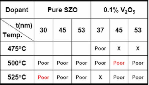
Table 3-1 The recipes for the device fabricated with pure SZO and 0.1% V-doped SZO. ○ ○ ○ 575oC ○ ○ ○ ○ ○ ○ 550oC ○ ○ ○ ○ ○ ○ 525oC ○ ○ ○ ○ ○ ○ ○ ○ 500oC ○ ○ ○ 475oC 60 53 45 37 30 60 45 30 t(nm) Temp. 0.3% V2O5 0.2% V2O5 Dopant ○ ○ ○ 575oC ○ ○ ○ ○ ○ ○ 550oC ○ ○ ○ ○ ○ ○ 525oC ○ ○ ○ ○ ○ ○ ○ ○ 500oC ○ ○ ○ 475oC 60 53 45 37 30 60 45 30 t(nm) Temp. 0.3% V2O5 0.2% V2O5 Dopant
Table 3-2 The recipes for the device fabricated with 0.2% V-doped SZO and 0.3% V-doped SZO.
Reference
[1] W. W. Zhuang, W. Pan1, B. D. Ulrich, J. J. Lee1, L. Stecker1, A. Burmaster1, D. R. Evans, S. T. Hsu, M. Tajiri, A. Shimaoka, K. Inoue, T. Naka, N. Awaya, K. Sakiyama, Y. Wang, S. Q. Liu, N. J. Wu, and A. Ignatiev, “Novell Colossal Magnetoresistive Thin Film Nonvolatile Resistance Random Access Memory (RRAM)”, in IEDM Tech. Dig., 2002, pp. 193-196.
[2] Jian-Gang Zhu and Youfeng Zheng, and Gary A. Prinz, “Ultrahigh density vertical magnetoresistive random access memory .invited”, J. Appl. Phys. , vol 87, 6668 ,2000.
[3] T. Y. Tseng, Extended Abstract of the First International Meeting on Ferroelectric Random Access Memories, Gotemba, Japan, 20, 2001.
[4] S. Lai and T. Lowrey, “OUM – A 180 nm Nonvolatile Memory Cell Element Technology for Stand Alone and Embedded Applicaions”, in IEDM Tech.
Dig., 2001, pp. 803-806.
[5] A. Beck, J. G. Bednorz, Ch. Gerber, C. Rossel,a) and D. Widmer, “Reproducible switching effect in thin oxide films for memory application”,
Appl. Phys. Lett., vol. 76, pp. 1324-1326, 2000.
[6] I. G. Baek, M. S. Lee, S. Seo*, M. J. Lee*, D. H. Seo*, D.-S. Suh*, J. C. Park*, S. O. Park, H. S. Kim, I. K. Yoo*, U-In Chung and J. T. Moon, ”Highly Scalable Nonvolatile Resistive Memory using Simple Binary Oxide Driven By Asymmetric Unipolar Voltage Pulses”, in IEDM
Tech Dig., 2004.
[7] R. Sezi, A. Walter, R. Engl, A. Maltenberger, J. Schumann, M. Kund, and C. Dehm, “Organic Materials for High-Density Nonvolatile Memory Apllication”, in IEDM Tech Dig., 2003, pp. 259-262.
[8] C. Rossel, G. I. Meijer, D. Bre´maud, and D. Widmer, “Electrical current distribution across a metal-insulator-metal structure during bistable switching,” J. Appl. Phys., vol. 90, pp.2892-2898, 2001
[9] T. Watanabe, J. G. Bednorz, A.Biestsch, Ch. Gerber, D. Widmer, A. Beck, S. J. Wild, “Current-driven insulator-conductor transition and nonvolatile memory in chromium-doped SrTiO3 single crystal,” Appl. Phys. Lett., Vol.
78, pp.3738-3740, 2001.
[10] S. Tsui, A. Baikalov, J. Cmaidlka, Y. Y. Sun, Y. Q. Wang, Y. Y. Xue, C. W. Chu, L. Chen, and A. J. Jacobson, “Field-induced resistive switching in metal-oxide interface,” Appl. Phys. Lett., vol. 85, pp.317-319, 2004.
[11] A. Baikalov, Y. Q. Wang, B. Shen, B. Lorenz, S. Tsui, Y. Y. Sun, Y. Y. Xue, and C. W. Cju, “Field-driven hysteretic and reversible resistive switch at