國立交通大學
電
機
與
控
制
工
程
學
系
碩
士 論 文
連續時間和差類比數位轉換器之迴圈延遲補償器設計
之研究
On Loop Delay Compensation Design for
Continuous-Time ΣΔ ADC
研 究 生:何峻徹
指導教授:董蘭榮 博士
連續時間和差類比數位轉換器之迴圈延遲補償器設計
之研究
On Loop Delay Compensation Design for
Continuous-Time ΣΔ ADC
研 究 生:何峻徹 Student:Jyun-Chen Ho
指導教授:董蘭榮 博士 Advisor:Lan-Rong Dung
國 立 交 通 大 學 電 機 與 控 制 工 程 學 系 碩 士 論 文 A ThesisSubmitted to Department of Electrical and Control Engineering College of Electrical Engineering and Computer Science
National Chiao Tung University In Partial Fulfillment of the Requirements
For the Degree of Master of Science
In
Electrical and Control Engineering September 2007
Hsinchu, Taiwan, Republic of China 中 華 民 國 九 十 六 年 九 月
On Loop Delay Compensation Design for
Continuous-Time ΣΔ ADC
Student:Jyun-Che
Ho Advisor:Lan-Rong Dung
Institute of Electrical and Control Engineering National
Chiao-Tung University
Abstract
A ΔΣ modulator is well-known as a very efficient technique for the implementation of high resolution A/D converters in low to medium bandwidth applications. Comparing with switched-capacitor (discrete-time) technique in the past, the continuous time circuitry is more suitable for today’s growing bandwidth applications. The thesis presents the implementation of a ΔΣ modulator with continuous-time techniques. Different numbers of digital delay in the ΔΣ feedback loop have been analyzed based on mathematic theorems in detail. The chip is designed with 1.8V power supply by using 0.18μm TSMC CMOS process, with
power consumption 6.5mW and the core area 0.05mm2. The simulation result shows
that the ADC achieves a 62dB peak signal-to-noise pulse distortion ratio (Peak-SNDR) within a 2MHz bandwidth with a sampling rate of 100MHz.
連續時間和差類比數位轉換器之迴圈延遲補償器設計
之研究
研 究 生:何峻徹
指導教授:董蘭榮 博士
國立交通大學電機與控制工程學系
摘要
和差調變器以往是非常廣泛的應用於低中頻寬、高解析度的一項技術。然而 相較於過去傳統所常用的交換型電容(離散時間)的技術,隨著對於頻寬需求的增 加,連續型的電路設計方式將會更適合於現今高頻寬的應用。本論文就實現連續 型和差調變器來做一些探討。在於和差調變器回授路徑上,不同的延遲時間將會 依據一些數學理論來做詳細地分析。此晶片使用台積電0.18μm CMOS 製程,供 應電壓為 1.8 V,消耗功率為 6.5-mW,晶片核心面積為 0.05mm2。模擬結果在 100MHz的取樣頻率、2MHz 的頻寬內得到峰值SNDR為 62dB。Acknowledgments
I would like to appreciate many people who help me in graduate studies in National Chiao-Tung University. First, I would like to thank my advisor, Professor Lan-Rong Dung, for his useful guidance and support. Without his inspiring discussions and strongly urge, this thesis is impossible to be done.
I would like to thanks all SoCLAB members for accompanying me in my graduate life. I relax my mind by sharing pleasure and pains with them. We not only research together but also play together. I also thank that they even give me some girls’ msn. I would like to thank Teng-Hung Chang for his useful suggests and comments in the meeting.
Finally, I would like to gratefully acknowledge my parents and my brother and sister. My family gives me a fine environment so that I could focus on research with my level best. Their love, care and patience are main motive power in the past two years.
Contents
ABSTRACT ... I ACKNOWLEDGMENTS... III CONTENTS... IV LIST OF TABLES ... VI LIST OF FIGURES... VI CHAPTER 1 ...1 INTRODUCTION ...11.1CONTINUOUS-TIME ΣΔMODULATORS...1
1.2ORGANIZATION OF THE THESIS...3
CHAPTER 2 ...4
FUNDAMENTALS OF ΣΔ MODULATORS ...4
2.1SAMPLING AND QUANTIZATION...4
2.2NYQUIST-RATE,OVERSAMPLING AND NOISE-SHAPING CONVERTERS...5
2.3ΣΔMODULATOR DESIGN ISSUES...6
2.3.1 Performance Increase in ΣΔ Modulators...6
2.3.2 Stability Constraints and Scaling...7
2.4CTLOOP FILTER SYNTHESIS...8
2.4.1 Equivalence between DT and CT...8
2.4.2 Rectangular Feedback Signal ...10
2.4.3 Decaying RC Feedback Signal...12
2.4.4 With an Additional Feedback Path...13
2.4.5 Design Examples...14
2.5ARCHITECTURES AND IMPLICIT ANTI-ALIASING FEATURE...20
2.5.1 Feed-Forward (FF) and Feedback (FB) Architectures...20
2.5.2 Implicit Anti-Aliasing Feature...21
CHAPTER 3 ...24
NON-IDEALITIES IN CT ΣΔ MODULATORS ...24
3.1.1 Gain Errors ...25
3.1.2 Finite DC-Gain ...26
3.1.3 Finite Gain Bandwidth...27
3.1.4 Further Filter Non-Idealities ...28
3.2ERRORS OF THE FEEDBACK DAC...29
3.2.1 Excess Loop Delay...29
3.2.2 Clock Jitter...30
3.2.3 Jitter Noise Power Analysis ...34
3.2.4 Jitter Noise Model...36
3.2.5 Further DAC Non-Idealities ...38
3.3ERRORS OF THE INTERNAL QUANTIZER...39
CHAPTER 4 ...40
ANALYSIS ON DIFFERENT LOOP DELAY COMPENSATION ...40
4.1EXCESS LOOP DELAY COMPENSATION...40
4.2NOISE POWER GAIN (NPG) ...42
4.2.1 Boundary of Noise Power Gain ...43
4.2.2 NPG Values of Different Delay Compensation...44
4.3POLE LOCATIONS OF NOISE TRANSFER FUNCTION...45
4.4THIRD ORDER SIMULATION RESULTS...47
4.5ANALYSIS AND SIMULATION RESULT OF OTHER HIGHER ORDER ΣΔMODULATOR...49
CHAPTER 5 ...56
A PRACTICAL CIRCUIT IMPLEMENTATION ...56
5.1LOOP FILTER IMPLEMENTATION...56
5.1.1 Active-RC Filter ...58
5.1.2 Bias Circuit ...60
5.1.3 Two-Stage Operation Amplifier...61
5.2TRI-LEVEL QUANTIZER AND DACREALIZATION...63
5.3CIRCUIT LEVEL SIMULATION RESULT...68
CHAPTER 6 ...72
CONCLUSION...72
List of Tables
TABLE 2.1CRFF THIRD ORDER MODULATOR DT AND CT COEFFICIENTS...16
TABLE 2.2CRFB THIRD ORDER MODULATOR COEFFICIENTS...18
TABLE 4.1COEFFICIENTS OF CRFF THIRD ORDER MODULATORS WITH DIFFERENT DELAY ...42
TABLE 4.2CRFF FOURTH ORDER MODULATOR COEFFICIENTS WITH DIFFERENT DELAY.50
List of Figures
FIGURE 2.1LINEAR QUANTIZER MODEL...5FIGURE 2.2BLOCK DIAGRAM OF ΣΔADC ...6
FIGURE 2.3DTΣΔ MODULATOR...9
FIGURE 2.4CTΣΔ MODULATOR...9
FIGURE 2.5CT RECTANGULAR FEEDBACK SIGNAL...11
FIGURE 2.6CT DECAYING RC FEEDBACK SIGNAL...12
FIGURE 2.7CTΣΔ MODULATOR WITH LOOP DELAY AND COMPENSATION PATH KB...14
FIGURE 2.8DTCRFF ...15
FIGURE 2.9CTCRFF ...15
FIGURE 2.10CRFF THIRD ORDER DT AND CTSIMULINK PSD(OSR=25) ...16
FIGURE 2.11DTCRFB...17
FIGURE 2.12CTCRFB...17
FIGURE 2.13THE RC DECAYING MODEL IN MATLAB/SIMULIK...19
FIGURE 2.14RC DECAYING WAVEFORM SIMULATIONS IN SIMULINK...19
FIGURE 2.15CRFB THIRD ORDER DT AND CTSIMULINK PSD(OSR=25)...20
FIGURE 2.16FIRST ORDER CTΣΔ MODULATOR...22
FIGURE 3.1AN ACTIVE RC INTEGRATOR WITH AN AMPLIFIER...24
FIGURE 3.2RC-VARIATIONS INFLUENCE OF A CT MODULATOR...26
FIGURE 3.3SNDR OF THE 3RD ORDER MODULATOR WITH FINITE GBW OPAMPS...27
FIGURE 3.4ILLUSTRATE OF NRZDAC PULSE WITH LOOP DELAY...29
FIGURE 3.5JITTER ERROR SOURCES IN CTΣΔ MODULATORS...30
FIGURE 3.6 (A)PULSE-DELAY JITTER (B)PULSE-WIDTH CLOCK JITTER...31
UNDER CLOCK JITTER INFLUENCE...32
FIGURE 3.8AΣΔ MODULATOR WITH SCR FEEDBACK...33
FIGURE 3.9IMPLEMENTATION OF THE SCR FEEDBACK CIRCUIT...33
FIGURE 3.10BLOCK DIAGRAM OF A CTΣΔ MODULATOR INCLUDING TIMING
UNCERTAINTIES...36
FIGURE 3.11FEEDBACK DACS TIMING ERROR...37
FIGURE 3.12THE BLOCK DIAGRAM OF A CTΣΔ MODULATOR INCLUDING AN ADDITIVE JITTER MODEL. ...37
FIGURE 3.13SNDR OF THE 3RD ORDER MODULATOR WITH THE JITTER NOISE MODEL...38
FIGURE 3.14RISE AND FALL TIME ASYMMETRY...38
FIGURE 4.1CTCRFF THIRD ORDER MODULATORS WITH DIFFERENT LOOP DELAY
COMPENSATION PSD IN SYSTEM LEVEL (OSR=25)...42
FIGURE 4.2THIRD ORDER NPG OF DIFFERENT DELAY COMPENSATION IN RC
VARIATIONS...44
FIGURE 4.3THE 3RD ORDER POLE LOCATIONS OF DIFFERENT DELAY COMPENSATION IN
RC VARIATIONS (BLUE LINES REPRESENT RC PRODUCT VARIATIONS FROM 0% TO
-40%.IN CONTRAST, RED LINES REPRESENT RC PRODUCT VARIATIONS FROM 0% TO
40%). ...46 FIGURE 4.4THIRD ORDER ΣΔ POLE DISTANCES FROM (0,0) WITH DIFFERENT DELAY
COMPENSATION...47
FIGURE 4.5RC-VARIATIONS INFLUENCE ON THIRD ORDER ΣΔ WITH DIFFERENT DELAY48
FIGURE 4.6WORST CASE OF RC-VARIATIONS INFLUENCE ON 3RD ORDER ΣΔ WITH
DIFFERENT DELAY COMPENSATION IN SYSTEM LEVEL SIMULATION...48
FIGURE 4.73RD ORDER HISTOGRAMS OF SNDR DEVIATIONS WITH ±30% PROCESS VARIATIONS...49
FIGURE 4.8CTCRFF FOURTH ORDER WITH DIFFERENT DELAY COMPENSATION PSD
(OSR=20)...50 FIGURE 4.9FOURTH ORDER NPG OF DIFFERENT DELAY IN RC VARIATIONS...51
FIGURE 4.10THE 4TH ORDER POLE LOCATIONS OF DIFFERENT DELAY IN RC VARIATIONS
(BLUE LINES REPRESENT RC PRODUCT VARIATIONS FROM 0% TO -40%.IN
CONTRAST, RED LINES REPRESENT RC PRODUCT VARIATIONS FROM 0% TO 40%).51
FIGURE 4.114TH ORDER ΣΔ POLE DISTANCES FROM (0,0) WITH DIFFERENT DELAY
COMPENSATION...52
FIGURE 4.12RC-VARIATIONS INFLUENCE ON FOURTH ORDER ΣΔ MODULATOR WITH DIFFERENT DELAY COMPENSATION...53
FIGURE 4.13WORST PERFORMANCE CASE OF RC VARIATIONS INFLUENCE ON FOURTH ORDER ΣΔ WITH DIFFERENT DELAY COMPENSATION IN SYSTEM LEVEL SIMULATION
FIGURE 4.144TH ORDER HISTOGRAMS OF SNDR DEVIATIONS WITH ±30% PROCESS
VARIATIONS...54
FIGURE 4.152ND ORDER HISTOGRAMS OF SNDR DEVIATIONS WITH ±30% PROCESS VARIATIONS...54
FIGURE 4.16THE CRITICAL ΔRC VALUES OF DIFFERENT DELAY COMPENSATION...55
FIGURE 5.1A CONTINUOUS TIME ΣΔ MODULATOR WITH ACTIVE-PASSIVE LOOP FILTER.56 FIGURE 5.2SIMPLIFIER SCHEMATIC OF A GM-C INTEGRATOR...57
FIGURE 5.3SIMPLIFIER SCHEMATIC OF AN ACTIVE-RC INTEGRATOR...58
FIGURE 5.4CAPACITIVE FEED-FORWARD FILTER IMPLEMENTATION IN ACTIVE-RC FILTER ...60
FIGURE 5.5BIAS CIRCUIT SCHEMATIC...61
FIGURE 5.6 TWO-STAGE OPAMP SCHEMATIC...62
FIGURE 5.7CMFB SCHEMATIC...62
FIGURE 5.8 COMPARATOR SCHEMATIC...64
FIGURE 5.9TRI-LEVEL QUANTIZER SCHEMATIC...64
FIGURE 5.10THE 1.5-BIT QUANTIZER SIMULATION RESULT...65
FIGURE 5.11THE EYE DIAGRAM OF THE 1.5-BIT QUANTIZER...66
FIGURE 5.12CTCRFF THIRD ORDER WITH DIFFERENT DELAY PSD IN CIRCUIT LEVEL (OSR=25)...67
FIGURE 5.13WORST CASE OF RC-VARIATIONS INFLUENCE ON 3RD ORDER ΣΔ WITH DIFFERENT DELAY IN CIRCUIT LEVEL SIMULATION...68
FIGURE 5.14SPICE CORNER SIMULATION...69
FIGURE 5.15TEMPERATURE SIMULATION...69
FIGURE 5.16CHIP LAYOUT OF A THIRD ORDER ΣΔ MODULATOR...70
FIGURE 5.17 (A)PSD AT FI=42.72-KHZ (B)PSD AT FI=1.2-MHZ...71
Chapter 1
Introduction
1.1 Continuous-Time ΣΔ Modulators
Data converter is one of the key components in electronic systems. Since the real world is inherently analog and the trend in voice, video, telecommunication, computer and many other applications is to get a digital form. The analog digital interfaces become critical paths. Data converters are composed of many analog building blocks such as operational amplifiers (opamps), track-and-holds and comparators, which make their design very challenging in high speed and low voltage design. Unlike Nyquist A/D converters, which need high-precision analog components, a sigma-delta (ΣΔ converter shows less sensitivity to analog circuit non-idealities. The most popular oversampling ADC architecture is based on a ΣΔ modulator. The ΣΔ A/D converter usually consists of an analog part called a ΣΔ modulator producing a bit stream followed by a digital part implementing decimation and digital filtering to complete the A/D conversion [1].
As decreasing supply voltage in recent CMOS technologies, it causes design on switched-capacitor (SC) circuit difficulty. Some problems will be found in SC circuit design such as high switch resistances limit the signal swing rang and also limit the sampling frequency. Some circuit techniques, like bootstrapping switch and switched–opamp, have been developed to overcome these problems. These techniques increase complexity in circuit design. However continuous-time (CT) ΣΔ modulators do not suffer these problems because they do not require precision track-and-hold
circuits. They take advantage of modern technologies with high speed but low precision capabilities [7, 8]. In SC circuit, input-signal sampling errors, like charge injection, settling-time errors and some other discrete time problems that do not exit in CT techniques. The gain bandwidth product (GBW) and slew rate requirements of the used opamps are much lower compared to their DT counterparts [2, 3, 4, 5]. Moreover, CT implementations of ADCs extend the input frequency range from a few 100 kHz up to a few 10 MHz [6]. Giving some examples, a CT complex sigma-delta multi-bit modulator, implemented in standard 0.25-μm CMOS technology and meeting all major requirements for application in IEEE 802.11a/b/g wireless LAN receivers was presented in [10]. The clock frequency is 320 MHz, producing an oversampling ratio of 16 for 20 MHz channel bandwidths and dissipates only 32 mW of power. Another wide bandwidth continuous-time ΣΔ ADC, operating between 20 and 40 MS/s output data rate, is implemented in 130-nm CMOS [11]. The ΣΔ ADC achieves 76-dB SNR 12 ENOB over a 20-MHz signal band at an OSR of 16. The power consumption of the CT ΣΔ modulator itself is 20 mW.
Furthermore, the sampling operation takes place inside the modulator. So sampling errors and out of band signals are greatly suppressed by the high gain loop filter. This thesis demonstrates a third order ΣΔ modulator with different compensation delays. It shows some practical advantages and drawbacks of a continuous time ΣΔ implementation, which have been proved by analysis and simulations.
1.2 Organization of the Thesis
This section gives a brief overview of the following chapters. Chapter 2 reviews some fundamentals of a ΣΔ modulator and introduces concepts of a CT ΣΔ modulator. Stability criteria in a ΣΔ modulator are also critically reviewed and perform equivalence between DT and CT modulator based on modified z transform. The method is general and systematic. Several low-pass design examples are given to illustrate the effectiveness of the transformation method.
Chapter 3 involves effects of circuit non-idealities and describes available error cancellation and compensation techniques. Some non-idealities models are also built for system level simulation.
Chapter 4 describes some methods to compensate for excess loop delay. Based on some stability theorems, different compensation delays and loop filter gain error relation have been discussed. It discusses the sensitivity of continuous-time modulators to the compensation loop delays.
Chapter 5 presents a circuit implementation of a CT ΣΔ modulator with quarter delay compensation. It concludes with simulation results of the entire ΣΔ modulator circuit with the active-RC amplifier.
Chapter 6 concludes the thesis and the main contributions could be summarized in this section.
Chapter 2
Fundamentals of ΣΔ modulators
2.1 Sampling and Quantization
The conversion of analog signal to digital domain can distribute into two basic operations: sampling in time and quantization in amplitude. In order to reconstruct the original signal without aliasing, an analog filter, called anti-aliasing filter, enforces the
Nyquist condition. The Nyquist theorem is fs≥2fB = fN, there f is the sampling s
frequency, f is the signal bandwidth and B f is the Nyquist frequency. N
The process of quantization in amplitude encodes a continuous range of analog values into a set of discrete levels. The key distinguish characteristic of a quantizer is its number of bits B, which correlates with the number of different output levels. If
the analog input is mapped into discrete levels, the quantizer is said to have
B-bits resolution. The quantizer step width is defined as 2B
2B 1
A
Δ =
− , showed in Fig. 2.1,
where A is the input signal full-scale. Because the quantizer is a nonlinear
component in the A/D converter, in order to analyze the quantization noise, the non-ideality must to be linearized. There is a basic of the additive white noise model for the quantizer [1]. Then, the quantizer is reduced to an unknown gain k and a
quantization error or noise . For analysis convenience, the quantizer gain has been
set to one, as indicated in Fig. 2.1. With this model, the quantization noise power and its noise power spectral density is derived to [1, 12]:
( ) e n 2 2 2 12 e e pdf dee σ ∞ −∞ Δ =
∫
= , 2 2 1 12 e S fs Δ = (2.1)Quantizer Δ x(n) y(n) + x(n) y(n) e(n) e(n)=y(n)-x(n)
Figure 2.1 Linear quantizer model
2.2 Nyquist-Rate, Oversampling and Noise-Shaping
Converters
The Nyquist ADC signal-to-noise-ratio (SNR) can be expressed as the following form:
| 6.022 1.76
p Nyquist
SNR =B dB+ dB (2.2)
From (2.1) it is obvious that an increase of the sampling frequency lowers the quantization noise power spectral density. By sampling higher than the Nyquist frequency and filtering the out-of-band noise. The quantization noise in the signal band can be reduced. This is main ideal of oversampling ADC. A ΣΔ modulator not only over-samples, but also shapes the quantization noise to out-of-band. Thus, the following filter called the decimator filters the out-of-band quantization noise. A typical block diagram of a ΣΔ ADC is given in Fig. 2.2. A ΣΔ modulator is the different transfer behavior for the quantization error signal, the noise transfer function (NTF) and the input signal, the signal transfer function (STF). Both equations are derived as: ( ) ( ) 1 , ( ) 1 1 ( ) 1 1 ( ) ( ) Y z STF z NTF z U z H z H z = = = + + (2.3)
By assuming the filter function in Fig. 2.2 to be a DT integrator 1 1
1 z z − − − , the 1 st order
in-band noise (IBN) yields: 2 2 2 2 2 3 1 4 ( ) 12 12 3 B B f f S S f INB df f f O π π − Δ Δ ≈
∫
= SR (2.4) H(z) + S/H Anti aliasing filter fs/2 fb DAC u(t) x(n) y(n) DigitalFilter SamplingDown
Delta-Sigma
Modulator Decimator
u(n)
Figure 2.2 Block diagram of ΣΔ ADC
Considering the extended general form to the N-order case, the equation (2.4) also could be derived as generally form:
2 2 12 1 12 3 N INB OSR π + Δ ≈ (2.5)
2.3 ΣΔ Modulator Design Issues
In this section, several design issues in design a ΣΔ modulator are presented. The order, oversampling ratio, and numbers of quantizer bits influence a ΣΔ modulator. Their stability constraints will also be described.
2.3.1 Performance Increase in ΣΔ Modulators
From (2.5) and the consideration above, there are several approaches to increase the performance of ΣΔ modulator. First, increasing the loop filter order, the operating principle of ΣΔ modulators is based on shaping the quantization noise from the in-band to higher frequency. It is obvious to use a more aggressive and higher order (N) filter function as in (2.5). By doing this, the decrease of the INB with the OSR in
through overloading the quantizer. Thus, in order to increase the stability, the loop filter coefficient should be scaling suitable [17].
From (2.5), it is obvious that using higher OSR will reduce the quantization noise. For higher OSR, the higher sampling frequency increases. From this consideration, analog components, like comparators, opamps and track-and-holds should be able to operate in the high frequency. The circuit realization is more difficult and the power consumption will increase.
Finally, reducing the quantization step width, that is to increase the quantizer number of bits. By doing this, the intrinsic resolution is increased proportionally
to . According to (2.5) the quantizer step width, as a symbol indicated in
(2.5), the quantizer noise power decreases proportionally. Furthermore, the incorporation of multi-bit internal quantizer tends to make higher order modulators more stable. Because the feedback DAC fed the modulator input, its errors are directly seen at the modulator input. For a single-bit internal quantize this problem does not arise, because a two level DAC is intrinsically linear. For a 1.5-bit tri-level quantizer, the DAC linearity also does not degrade the modulator performance seriously [15].
2
(2B−1) Δ
2.3.2 Stability Constraints and Scaling
The drawback of single-loop single-bit ΣΔ modulators with order higher than
2nd is their tendency to instability. The stability is defined as a modulator normal
operating condition. All integrator outputs remain bounded over time with bounded input [1, 16]. In order to ensure the ΣΔ modulator operates stably, having chosen an optimized noise transfer function (NTF) to meet the specification. The analysis of stability is also important. Therefore, several methods can be used, among others simulation or calculation. The method of root-locus plots has been
commonly adopted to analyze the stability. For the unknown quantizer gain k, which has no definition in the case of a single-bit ΣΔ modulator, has been assumed as a variable gain when performing the root-locus analysis. Avoiding overloading the integrator output could sustain system stability [16].
2.4 CT Loop Filter Synthesis
In fact, CT ΣΔ modulators are mixed CT-DT systems. While the input signal is continuous and the loop filter is composed of CT integrators, the output signal is sampled. The feedback DAC signal can either have a constant output during each clock cycle (NRZ case), or have its output decay exponential (SCR case). Different feedback DAC waveforms make the calculation of the CT ΣΔ modulator loop filter coefficients difficult. The NTF is usually designed in such a way that the in-band quantization noise is sufficiently low to be neglected compared to the circuit transistors noise. After calculations of the proper CT coefficients required to obtain the desired NTF, these coefficients should be scaled for maximum output swing of the integrators.
In order to overcome problems associated with the design and analysis of mixed CT-DT systems, CT ΣΔ modulators can be designed entirely in the DT domain. A DT-to-CT transformation method can then be applied in order to obtain the equivalent CT ΣΔ modulator.
2.4.1 Equivalence between DT and CT
A general DT ΣΔ modulator is showed in Fig. 2.3, where is the DT loop
filter. A general CT ΣΔ modulator is also showed in Fig. 2.4, where ( ) d H z ( ) c H s is the CT
design the CT loop filter for given a feedback DAC and makes the
(2.6) ( )
c
H s HDAC( )s
CT loop gain equals to DT loop gain This can be expressed as below.
her ( ) c G z G z . d( ) ( ) ( ) ( ) ( ) ( ) ( ) ( ) [ ( ) ( )] d c d c d c d c DAC G z G z X z X z Y z Y z G z z H s H s = = = eG zd( )=H zd( ) w Quantizer U(s) + H Y(z) d(z) Xd(z) U(z) fs Figure 2.3 DT ΣΔ modulator f U(s) + Hc(s) Xc(s) Y(z) HDAC(s) S Xc(z) Figure 2.4 CT ΣΔ modulator
Previous work on ΣΔ DT-CT equivalence has usually solved (2.6) in the tim domain using the following relations
e hip:
1[ ( )] [ ( ) ( )]
d c DAC
Z G z− = H s H s (2.7)
This transformation between DT and CT domain is called impulse invariant
transformation, because it makes the open-loop impuls samp
e responses equal at the ling times. Both modulators will produce the same output bit streams if we ensure that the inputs to their quantizers are the same, each quantizer would then make the same decision. Therefore two modulators are equivalent, if for the same input waveform, their quantizer input voltages at sampling instant are equal.
The complicated mathematics involved in the computation of time-domain convolution make this method not adapted to design systematically and has usually been
ularity problems and the use of special control and
lished [6, 22]. This will probably be the upcoming method since it
thematics necessary to pe
2.4.2 Rectangular Feedback Signal
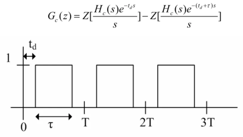
During a period T, the rectangular feedback signal, show in Fig. 2.5, can be describe in time-domain by following relationship:
used for specific cases [18, 19].
A more general transformation method, using state-space has been presented in [20]. Heavy use of matrix notation, sing
optimization Matlab functions [21] make the use this transformation technique rather difficult.
Beside the DT-CT conversion, directly design a CT loop filter from its desired NTF is also pub
allows the optimization of the CT loop filter until it shows sufficient robustness against process variations, excess loop delay and clock jitter [6].
In this work we perform the DT-CT equivalence directly in the z-domain using modified -z-transform technique. While avoiding the complex ma
rform time-domain convolution, this technique enables us to get the z-transform of signals having variations between two sampling instants. By using this method, the feedback DAC can be RZ or NRZ and the shape of the feedback signal can either be rectangular or non-rectangular.
hdac( )t =u t t( − d)−u t t( − − d τ)
whereu t( ) is unit step function. The following equa
(2.8) tion is derived by applying the . Laplace transform ( ) ( ) d d t s t s e e H s τ − − − + = (2.9 DAC s )
The z-transformation of the CT ΣΔ loop gain can be expressed by
[ d( )] [ c( ) DAC( )]
Z G z =Z H s H s (2.10)
Substituting (2.9) into (2.10) results in
( ) ( ) ( ) ( ) [ c c G z =Z d ] [ d ] t s t s c H s e H s e Z s s τ − − + − (2.11)
Figure 2.5 CT rectangular feedback signal Equation (2.11) is rewritten in following form:
1 ( ) [ c ] c m H 2 ( ) ( ) [ c ] m s H s s (2.12) where G z Z Z s = − 1 1 d t m T = − and 2 ( ) 1 td m T τ + = − . In order to design valent to a ΣΔ modulator,
starting from the Laplace repres
a CT ΣΔ modulator which
is equi DT we use equation (2.12) and (2.6) to get the
general expression for DT-CT equivalence.
The method to calculate the modified-z-transform
entation is the Residue theorem. This method is systematic and more convenient for design automatic. Equation (2.12) can be written in the following form:
1 1 2 2 ( ) at pi ( ) Residues of c m Ts m Ts c c Ts H s G z s z e − = −
∑
pi pole of ( ) at pi pi pole of ( ) ( ) Residues of c s m Ts m Ts c Ts H s s H s e e H s e e s z e = − = − −∑
(2.13)Using (2.13) the loop gain of the CT ΣΔ can be expressed in DT z domain.
could be obtained. In a special case of a NRZ feedback signal, with
( )G z c
Comparing coefficients of the numerator and the denominator of G z with those c( )
of the DT loop gainG z , the coefficients of CT loop filterd( ) H s c( )
0
d
substitution in (2.9), we have a well-known zero-order-hold relation: 1 ( ) e Ts H s − − = (2.14) DAC s
2.4.3 Decaying RC Feedback Signal
In fact, the rectangular feedback signal is commonly used in CT modulators. It is useful to design feedback with non-rectangular signals. First, it can be used to model
RC signal is shown in Fig. 6.
idealities in the rectangular feedback, such as non-zero rise and fall time. The second is that the non-rectangular feedback shape is possible to reduce the modulator sensitivity to clock jitter noise (in this thesis section 3.2.2).
In this section we show the DT-CT transformation can be used for CT ΣΔ modulators with decaying RC feedback signals. A decaying
2.
T
2T
3T
t
dt
Figure 2.6 CT decaying RC feedback signal
Using the same method as described in section 2.4.2, the decaying RC feedback signal can be written in the time-domain by the following relationship:
1( )
( ) RC t td [ ( ) ( )]
hdac t e u t td u t td τ
− −
= − − − − (2.15)
The following equation is derived by applying the Laplace transform.
( ) ( ) 1 RC DAC H s s d d t s t s RC e e e RC τ − τ − − − +
Substituting (2.16) into (2.10) results in =
+
( ) ( ) ( ) [ ( )] [ ] [ ] 1 1 d d t s t s c c RC c H s e H s e Z G s Z Z e s s RC RC τ τ − − − + = − + + (2.17)
Using the Residue theorem, (2.17) could be derived in the following form:
1 2 ( ) H s ( ) ( ) [ ] [ ] 1 1 c RC c c m m H s G z Z e Z s s RC RC τ − = − + + (2.18) where 1 1 d t m 2 ( ) 1 td m +τ T = − and T
= − . The modified z transform can be calculated
using Residue theorem method as describe in (2.13).
2.4.4 With an Additional Feedback Path
Loop delay is one of the major sources of instability and performance ainly due to the comparator in the quantizer. It is also due to the propagation delay in the digital circuitry required to perform Dynamic Element Match
In this section, we put an explicit delay of one period degradation in CT ΣΔ modulators. Loop delay is m
response time and the latch propagation delay
ing (DEM) of the feedback DAC elements in the case of multi-bit ΣΔ modulators. A loop-delay compensation is suggested to add an additional feedback signal into the quantize input, as indicated in Fig. 2.7 [2, 23].
1 d t T period, = , or half a 0.5 d
T = in the feedback loop. This delay should be sufficiently large to
include comparator and digital circuitry delay with enou
t
gh margins to include addit
fixed half period delay or unit period delay in the feedback path can be introduced by a synchronization latch. The compensation coefficient kb is calculated by comparing
(2.19)
ional delay due to signal dependency, process or temperature variations. The
loop gain transfer function G z and( ) G z , as written below: ( )
( ) ( ) ( ) [ ( )( ( ))] d c d DAC b c G z G z H z z H s k H s = = + d c
Y(z) +
H
c(s)
Xc(s) fs Xc(z) U(s) +H
DAC(s)
L
td/T
oop delay
KbFigure 2.7 CT ΣΔ modulator with loop delay and compensation path Kb The loop gain transfer function with loop-delay compensation could be written in the following form: 1 ( ) [ T ( ( ))] c b c G z z e k H s s = −e−Ts −tds + (2.20)
Using the modified-z-transform and Residue theorem, we get:
1 ( ) at pi pi pole of ( ) ( ) (1 ) Residues of b c mTs b c c Ts k H s s k H s e G z z s z e + − = + = − −
∑
(2.21) inator of abovewith those of the DT loop gain , the coefficients of the CT loop filter and
compensate kb coefficient could be obtained.
ΣΔ from well-known DT toolbox. Without loss of generality, two main topologies:
nators Feed-forward Form, Fig. 2.8 and Fig. 2.9 z
oolbox [21]. Using the design procedure written in above section, the CT
Comparing the coefficient of the numerator and the denom G z c( )
( )
d
G z H sc( )
2.4.5 Design Examples
In this section we show a systematic design approach to calculate CT
z CRFF: Cascade of Reso
CRFB: Cascade of Resonators Feedback Form, Fig. 2.11 and Fig. 2.12 The DT ΣΔ coefficients have been obtained using Richard Schreier’s ΣΔ T
obtain for NRZ and decaying RC signals. − 1 z z bn −1 n b −2 n b 3 b + + 2 b 1 b + − 1 1 z + U(z) Y(z) − 1 1 z − 1 z z − 1 1 z X(z) − 2 1 − 2−1 2 n gd gd Figure 2.8 DT CRFF n a −1 n a −2 n a 3 a 2 a 1 a 1 sT − − 2 1 2 n gc − 2 1 gc 1 sT 1 sT 1 sT 1 sT ( ) DAC H s Figure 2.9 CT CRFF
We take CRFF third order, OSR=25 as an example. From the DT ΣΔ Toolbox
we could get the DT ΣΔ co (2.13), (2.21) with DT ΣΔ
coefficients, the CT ΣΔ coefficients could be obtained. This design procedure has been
, efficients. Comparing
implemented using the symbolic mathematical tool MAPLE. We could get the different CT ΣΔ coefficients with different feedback DAC waveforms. The CRFF third order modulator coefficients are listed in following Table 2.1. In order to prevent too large signal swing in the integrators, we let all integrator coefficients equal to 0.5 in the CTΣΔ modulators.
Table 2.1 CRFF third order modulator DT and CT coefficients DT CT NRZ (with td=0) CT NRZ (with td=0.5) b1 0.752 a1 2.0247 a1 2.606 b2 0.574 a2 2.294 a2 2.605 b3 0.156 a3 1.246 a3 1.246 gc2 0.038 gc2 0.038 gd2 0.01 kb 0 kb 0.581 104 105 106 107 108 -140 -120 -100 -80 -60 -40 -20 0 DT SNDR : 66.2dB CT(td=0) SNDR : 67.1dB CT(td=0.5) SNDR : 67.0dB
Figure 2.10 CRFF third order DT and CT Simulink PSD (OSR=25)
In order to study the behavior of the resulting CT ΣΔ modulators, the Matlab/Simulink simulations have been performed to compare them with DT ΣΔ. Fig
2.10 show ulators.
It is
. s the power spectral density (PSD) of the DT and calculated CT mod
obvious from Fig. 2.10 the CTΣΔ modulators using the coefficient calculated using DT-to-CT transformation method are equivalent to the original DT ΣΔ
modulator.
Using the same method, we can also get the coefficients in the CRFB topologies with different feedback shapes those are rectangular or decaying RC waveforms. The CRFB topologies are shown as Fig. 2.11 and Fig. 2.12.
+ + + U(z) Y(z) − 1 1 z − − 2 1 2 n gd − 2 1 gd − 1 1 z − 1 1 z − 1 z z − 1 z z DAC X(z) + + 1 a a2 a3 an−1 an 1 b b2 b3 bn−1 bn Figure 2.11 DT CRFB + + + U(s) Y(z) 1 sT − − 2 1 2 n gc − 2 1 gc 1 sT 1 sT 1 sT 1 sT DAC X(s) X(z) 1/T + + 1 a a2 a3 an−1 an 1 b b2 b3 bn−1 bn Figure 2.12 CT CRFB
Comparing (2.13), (2.18) with DT ΣΔ coefficients, the CT ΣΔ coefficients could also
be obtained. The CRFB CT ΣΔ ith different feedback shapes
re listed in Table 2.2
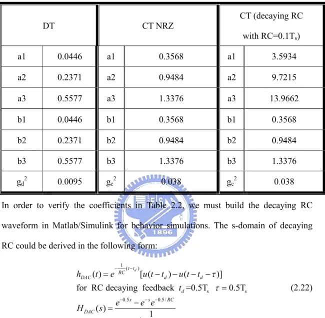
modulator coefficients w a
Table 2.2 CRFB third order modulator coefficients DT CT NRZ CT (decaying RC with RC=0.1Ts) a1 0.0446 a1 0.3568 a1 3.5934 a2 0.2371 a2 0.9484 a2 9.7215 a3 0.5577 a3 1.3376 a3 13.9662 b1 0.0446 b1 0.3568 b1 0.3568 b2 0.2371 b2 0.9484 b2 0.9484 b3 0.5577 b3 1.3376 b3 1.3376 gd2 0.0095 gc2 0.038 gc2 0.038
In order to verify the coef in Table 2.2, we must build the decaying RC
waveform in M imuli or behavio tions. The omain of decaying
RC could be derived in the following form: ficients atlab/S nk f r simula s-d 1 ( ) s s 0.5 0.5/ ( ) [ ( ) ( )]
for RC decaying feedback =0.5T 0.5T ( ) 1 d t t RC DAC d d d s s RC DAC h t e u t t u t t t H s s e e e RC −
Because quantizer outputs must pass through a track-and-hold, the decaying RC derived from the combination of s-domain and z-domain could be shown as:
τ τ − − − − − = − − − − = = + (2.22) & 0.5 1 0.5 / ( , ) Ts RC z z e s RC s z s 1 ( ) ( , ) ( ) 1 1 T H DAC H s RC s z H s z RC − − − − = − = + (2.23) −
rom above (2.23), we can easily build the decaying RC model in Matlab/Simulink, F
as indicated in Fig. 2.13.
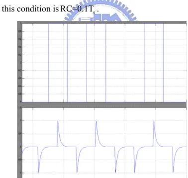
Figure 2.13 The RC decaying model in Matlab/Simulik
The simulation result of the decaying RC waveform is shown in Fig. 2.14, where the
value of RC in this condition isRC=0.1T .s
Figure 2.14 RC decaying Waveform simulations in Simulink
Fig. 2.15 shows the PSD of the CRFB third order ΣΔ of the DT and calculated CT modulators. It is obvious from Fig. 2.15, the CT ΣΔ modulators with rectangular and
non-rectangu lated using
DT-to-CT transformation method is equivalent to the original DT ΣΔ modulator. lar (decaying RC) feedback signals using the coefficient calcu
Figure 2.15 CRFB third order DT and CT Simulink PSD (OSR=25)
2.5 Architectures and Implicit Anti-Aliasing Feature
In this section, the differences of the most typical architectures (CRFF in Fig. 2.9,
CRFB in ote that
2.5.1 Feed-Forward (FF) and Feedback (FB) Architectures
h-pass filters with less attenuation in the signal band going from the first stage to the last one. Therefore, the first stage variable will contain only a very small component of the input signal and a large amount of filtered quantization noise
Fig. 2.12) for the implementation CT ΣΔ modulator are present. N
the CRFF has been derived from the CRFB by applying the flow graph reversal procedure [24].
For a feed-forward architecture, the signal and noise transfer functions are identical, being hig
components, but only out-of-band distortions. The last integrator will introduce the large amount of in-band distortions, but these will be shaped by the loop filter. For this topology, only the linearity of the input integrating stage is critical, all others are not detrimental to SNDR. However the feed-forward architecture shows reduced anti-aliasing behavior and in addition a strong STF peaking around the cutoff frequency.
In the case of CRFB topology, each state variable will contain some filtered quantization noise plus a filtered version of the input signal. Since the output of an integrator represents the input of the subsequent integrating stage, it follows that the linearity of the first integrating stage is more critical than the linearity of the final one. For
ach adds a zero to the STF
2.5.2 Implicit Anti-Aliasing Feature
the CRFB topology, the linearity of integrators is important for all stages. The second integrator requires almost the same linearity as the first one, and the specifications for the subsequent stages can be eased as one approaches the quantizer.
In the CRFF topology, the influence of the input integrator non-linearity is the same as in the case of CRFB topology, but the linearity of all other stages is not affecting SNDR to suck great extent. The STF of the feedback-compensated modulator has a flat response providing filtering to interferers.
Thus, in order to get a power efficient ΣΔ modulator while maintaining a good filtering characteristic, a combination of FF and FB has become popular [11]. In [11] the feedback path to the output of the first integrator has been replaced by a feed-forward path. As a consequence, the feed-forward appro
and resulted in reducing the filtering by one order and introducing a small peak near the cutoff frequency.
s f
tones which differ in frequency by a multiple of are indistinguishable from one
another and so overlap in a spectral plot. This is usually referred to as signal
aliasing. DT ΣΔ modulators usually require an extra filter to be placed prior to their inpu
problem
t to bandlimit the input signal and hence reduce the problem of aliasing. An implicit feature of CT ΣΔ modulators is that they have some built-in anti-aliasing protection.
It is easy to understand this intuitively by taking a first order low pass CT modulator as an example. In Fig. 2.16 the quantizer input in the z domain obeys the following relation: ( 1) 1 ( 1) ( ) ( ) s ( ) s n T nT s x n x n y n u t T + + = − +
∫
dt (2.24) 1/Ts + u(t) 1 y(n) s sT ( ) DAC H s x(t) x(n)Figure 2.16 First order CT ΣΔ modulator
Notice that the input signal is integrated over one clock period prior to being sampled. The input is multiplied by a rectangular pulse. We may also write that input integral as a convolution of the input with a rectangular pulse:
( 1) ( ) ( ) ( , ( 1) ) s n T s s s u t dt u t rect nT n T + = ∗ +
∫
( ) sin ( ) nTultiplication in the frequency domain. Equation (2.25) tells us that the input spectrum is multiplied by the spectrum of a rectangular pulse, namely, a sinc function. This latter function has spectral nulls
s f
U s c
f
= ⋅ (2.25)
at frequencies . We are concerned about signals near multiples of the sampling frequency, which would alias to near dc, and that sig
the sinc. In a CT modulator, the anti-aliasing property arises because the sampling
plicit antia
, 1
s af a
± ≥
nals are attenuated by
happens after the integrator.
We would expect higher order modulators to have more antialias protection because they have more integrators before the sampler. In the general case, it has been
shown that the im lias filter for a CT ΣΔ can be plotted against frequency
w
by evaluating [19]. ( ) (exp( s)) jw HH
jwT ∧ , (2.26)Chapter 3
Non-idealities in CT ΣΔ Modulators
In this chapter, we consider some non-idealities in CT ΣΔ circuit implements. We
survey the literature on the perfo ealities in CT ΣΔ modulators
and summarize the results that are germane to the design of CT ΣΔ modulators.
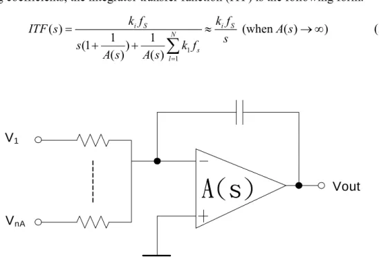
3.1 E
-RC integrators are considered, as showed in Fig. 3.1, shows a typical schematic with
ith ki being the integrator scali
rmance effect of non-id
rrors of the Filters
The loop filter transfer function is the major performance determining part of a ΣΔ modulator, because it defines the NTF and therewith the quantization noise-shaping behavior. Without loss of generality, in the following active
A n inputs and with an amplifier transfer function A(s). W
ng coefficients, the integrator transfer function (ITF) is the following form. 1 1 ( ) (when ( ) ) (1 ) ( ) ( ) i S i S N s l k f k f ITF s A s s k f A s A s = 1 1 s = ≈ → ∞ + +
∑
(3.1)A(s)
V1 VoutFigure 3.1 An active RC integrator with an amplifier
3.1.1 Gain Errors
Gain errors in CT modulators are more serious than an order of magnitude larger than in SC implements, because the integrator gains are mapped into capacitor relative ratios. These are intrinsically precise and variations are lower than 0.1% typically. In CT ΣΔ modulators integrator gains are mapped into resistor-capacitor
product, which l ±30%.
It has been frequently reported that integrator gain variations have serious influence on single-loop ΣΔ modulators. A negative shift of the integrator gain yields less
ction of argely vary over process and temperature by values of
aggressive noise-shaping behavior and thus slightly higher IBN. In contrast, a positive shift of the integrator gain yields more aggressive noise-shaping, but this effect could lead to instability of the modulators. The time constant of the active-RC integrator is determined by the absolute product of the resistor and capacitor. It is possible to avoid this sensitivity by moving the poles of the signal transfer fun
the modulator to cover a greater range of the RC-variation with a stable modulator [26]. The influence on the in-band quantization noise can be calculated from Equation
(3.2), where ΔRC is the RC-variation value and
a
1 is the first integrator coefficient.6 2 6 2 7 1 (1 ) 84 RC IBN ≈π Δ + Δ (3.2)
In Fig. 3.2 it is shown that RC variations influence on the CT ΣΔ modulators, which using NRZ half delay feedback, the coefficients as list in Table 2.1. Consequently, time constant tuning may become necessary [6, 11, 26]. Assume a reference clock is well defined, stable and low jitter, a simpler trimming of integrator time constants can be accomplished by digitally programming binary weighted capacitor arrays with switches [11]. In [26] a capacitive tuning is proposed to achieve
a OSR
For cascaded modulators, the behavior is even worse. Since these architectures depend on matching between analog and digital transfer functions. Nonetheless, a digital correction is possible and recent implementations prove the approach [27].
-0.4 -0.2 0 0.2 0.4 35 40 45 50 55 60 65 70 75
RC Variation
SN
D
R
[
d
B]
Figure 3.2 RC-variations influence of a CT modulator
3.1.2 Finite DC-Gain
Finite dc-gain shows the same effect as in DT implementations. Finite dc-gain causes the NTF zeros are moved away from dc to higher frequency as do the poles of the filters. In presence of a finite opamp gain can express in the following form [28]:
2 6 2 7 1 1 21 [ ] 12 7 5 v IBN a OSR OSRA π Δ ≈ + 2 (3.3)
The critical gain of a 3rd order ΣΔ modulator is equal to
,3 21 5 v dB OSR A π ≈ (3.4)
3.1.3 Finite Gain Bandwidth
er GBW of the opamps. This has been attributed to the lack of the high current peaks of SC implemented DT
circuits. Nevertheless, in [29] for a 3rd order modulator a margin of around 1.5fs was
r non-dominant pole of 2-3 times the sampling frequency. Recently, [31] a finite amplifier model was introduced. With
and
CT implementations are claimed to work with low
found; [30] claimed an integrato
dc A GBW =A w ( ) 1 dc A s w + A
A s = from (3.1), the ITF can be derived as:
( ) 1 j s j s GBW i j s GBW GBW k f k f ITF s GBW k f + = ⋅ s s + +
∑
∑
(3.5)nce of finite GBW is in first order appro
Consequently, the non-ideal influe ximation a
gain error and a non-dominant pole. For rectangular feedback the non-dominant pole can be modeled as feedback delay. Thus, compensation is possible as correction of
gain errors and excess loop delay [32]. In Fig. 3.3 the integ it fin
simulated for NRZ feedback pulse form.
rator w h ite GBW is 0.5 1 1.5 2 2.5 3 35 40 45 70 65 50 55 60 GBW / fs DR
Figure 3.3 SNDR of the 3rd order modulator with finite GBW opamps
S
3.1.4 Further Filter Non-Idealities
Beside finite dc-gain and bandwidth in opamps, many other filter non-idealities exist, while a short overview is given here:
Finite slew rate is a nonlinear effect and causes distortion as well as an increase of the noise floor: in DT implementations signal transitions are very fast SC-pulses and finite slew rate yields incomplete signal settling. By using CT circuitry, the slew rate specifications can be relaxed. This is because in CT modulators the signals changed
Circuit noise is generally designed as the dominant noise source in a ΣΔ modulator. The main contributor is the first integrator. There exists no sampling capa
bias current. The circuit noise and power relat
much more slowly than DT ones.
citor in CT ΣΔ modulators. For the low noise consideration, this requires larger transconductances and consequently higher
ion was written in following form:
n2 1 1 m DS g v I ∝ ∝ (3.6)
The input referred noise power density is approximately in the following relationship:
2 , , 2 , 2 f 8 ( ) 3 e f e th DAC in ox K n n R gm C WLf + + (3.7) Note tha i in S = kT R +
t since the noise is not sampled until it has been filtered. The aliased noise components are attenuated by noise-shaping. Therefore, the input referred noise power that appears in the signal band is equal to:
2 i 2 8kTa nf OS , 1 2 ( ) 3 in therm in DAC in v R R R R C gm = + + ⋅ (3.8)
We require smaller resistances ( Rin and Rdac respectively) and a larger
transconductance and consequently higher bias current in low circuit noise design. Non-linearities of the first filter stage are similarly important as the linearity of
the feedback DAC. The voltage dependency of the amplifier dc-gain, the output impedance and the integrator resistors may introduce substantial distortion especially
put stage. The limited output swing, also know as clipping, is a signal-dependent variation of the system
increased the
3.2
ifts the DAC pulse into the next sampling instant. This is the case for NRZ DAC with any delay, shown in Fig. 3.4.
at larger input amplitudes. To reduce non-linearities, the input resistors should be as large as possible [33], limited by thermal noise. Also, increasing the bias current in the differential pair improves the linearity of the in
states from their
ideal values and results in severely signal band noise as well as
distortion.
Errors of the Feedback DAC
3.2.1 Excess Loop Delay
In [2, 7] timing non-ideality known as excess loop delay was considered. The excess loop delay can arise from two different effects:first, due to a finite respond time of the DAC output to the clock edges and its input [7];Second, due to a designed delay between the quantizer sampling edge and the subsequent latch feeding the DAC, The delay sh T td Quantizer clock DAC clock
Figure 3.4 Illustrate of NRZ DAC pulse with loop delay
Excess loop delay is a serious non-ideality because it alters the equivalence between the CT and DT representations of the loop filter and causes the numerator
order of transfer function increases by one. Its effect on performance is severe if the sampling clock speed is an appreciable fraction (10% or more) of the maximum transistor switching speed. This is becoming more likely nowadays as desired conversion bandwidths increase and a ΣΔ modulation with an aggressively high clock rate relative to the transistor switching speed is considered for the converter architecture [34].
3.2.2 Clock Jitter
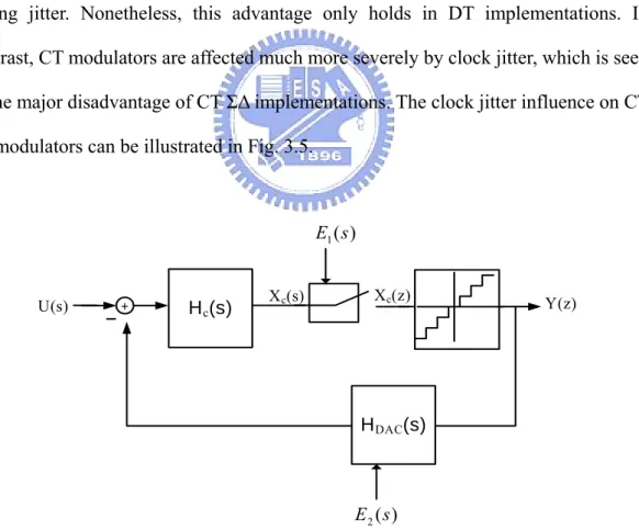
Clock jitter, that is statistical variations of the sampling frequency, depends on the purity of the clock source. In the past, ΣΔ modulators were found to be tolerant to timing jitter. Nonetheless, this advantage only holds in DT implementations. In contrast, CT modulators are affected much more severely by clock jitter, which is seen as the major disadvantage of CT ΣΔ implementations. The clock jitter influence on CT ΣΔ modulators can be illustrated in Fig. 3.5.
U(s) + Hc(s) Xc(s) Y(z) H 1( ) E s Xc(z) DAC(s) 2( ) E s
Figure 3.5 Jitter error sources in CT ΣΔ modulators
There are two different sources of clock jitter errors (E1 and E2) in the modulator
suppressed by the modulator loop. The dominant jitter error in CT implementations
appears through the feedback DAC error E2. A CT ΣΔ modulator integrates the
feedback waveform and a statistical variation of the feedback results in a statistical integration error and in increased noise.
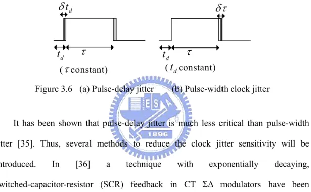
The random variation in the delay time td is called pulse-delay jitter and the
random variation in pulse-width τ is called pulse-width jitter. These two types of jitter are illustrated in Fig. 3.6.
d
t
δ
τ
dt
( constant)τ
dt
δτ
( constant)τ
dFigure 3.6 (a) Pulse-delay jitter (b) Pulse-width clock jitter
It has been shown that pulse-delay jitter is much less critical than pulse-width jitter [35]. Thus, several methods to reduc
t
e the clock jitter sensitivity will be
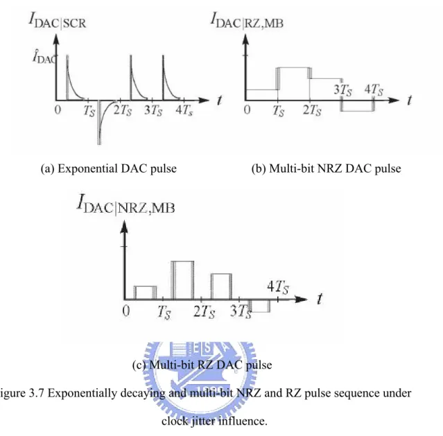
following, different feedback waveforms like sinusoid [37], linear or quadratically decaying were proposed [38]. Beside this, multi-bit DAC implementations also reduce the jitter sensitivity. This is because that the smaller step size reduced the charge error. But it must be noted that only NRZ
multi-bit feedback effectively reduces clock jitter noise, but not the o ploy RZ
multi-bit fe
introduced. In [36] a technique with exponentially decaying, switched-capacitor-resistor (SCR) feedback in CT ΣΔ modulators have been employed, as shown in Fig. 3.7a .In the
ften em edback, as illustrated in Fig. 3.7b, 3.7c.
(a) Exponential DAC pulse (b) Multi-bit NRZ DAC pulse
(c) Multi-bit RZ DAC pulse
Figure 3.7 Exponentially decaying and multi-bit NRZ and RZ pulse sequence under clock jitter influence.
In order to reduce the large sensitivity to jitter, [48] also proposed to use SC pulse in a CT modulator. SC feedback is usually adopted in DT charge integrators. In the CT domain, the integration is done over one clock period. Thus, the pure charge
feedback is not directly appl e feedback pulse over time,
a
shown exemplarily in Fig. 3.8, whe amed SCR feedback. Due to
s influence on the feedback pulse shape, the additional resistor also allows the efin
icable. To be able to define th
n SC is combined with an additional series resistor. The resulting architecture is re the DAC circuit is n
it
d ition of the jitter sensitivity over the feedback time constant and reduces the
RC R CR R bTS
τ = = (3.9)
Note that, the
τ
RC lowest limit is the switch turn on resistorr
on. Ifron >RR, then theRC
τ time constant will be dominant by switch turn on resistor r [36]. on
Q ua ti zer n CLK Out A1
fs
C1R
R refV
±
RC
Figure 3.8 A ΣΔ modulator with SCR feedback
Ref V + Ref V − Charge Charge Discharge Discharge fb i CM V R C R R Amplifier input
Figure 3.9 Implementation of the SCR feedback circuit
A unit of SCR feedback DAC cell as in Fig. 3.9. Principally the SCR feedback
DAC has two modes of operation: first charging the capacitors to either the
positive or negative reference voltage, depending on the quantiz igital output
signal , and then discharging the capacitors over the resistors
R C er d
out
the integrators. To simplify the system design, these phases were chosen equal to the system clock phases. We take the first half of the clock cycle to charge the feedback capacitors, depending on the comparators output, and discharge it in the second half,
translating into a feedback pulse position. Here the capacitor is charged on either
positive or negative reference voltage when
R C
Charge=Clk V⋅ out is high. It is
discharge over R to the integrator input when R Discharge=Clk
fits of mu
Response (FIR) DAC can be used in as bit and the DAC respons
is high.
In order to have the jitter relaxation bene ltilevel DAC while
maintaining high linearity, Finite Impulse reported in [39,49]. The quantizer is one
over n clock cycles and the jitter contri ately averaged over n
periods. In [
y the pulse-width clo odulator in the
e pulse is widened bution is approxim
39] it is reported that using 9-level instead of 2-level DAC reduces the jitter noise contribution by 18dB. By using this FIR DAC method, it also increased loop delay and lead to stability problem.
3.2.3 Jitter Noise Power Analysis
The pulse-width jitter has a much more degrading effect on the SNR than the pulse-delay jitter. In the following analysis, we will neglect the pulse-delay jitter and only the pulse-width jitter will be taken into account.
In order to calculate the noise power generated b ck jitter, let
us look at the output of the first integrator of the m ideal case.
1 d d t s s t T T τ τ + 1 dt=
∫
(3.10)If the pulse-width has an error ofδτ, the output of the first integrator will be
1 d d t s s t T T τ 1 dt δτ τ τ + = +
∫
(3.11)δτ The error in the output of integration is then equal to
τ . Assuming that the clock
δτ with variance 2
j
σ , we can say that the jitter noise
jitter causes timing errors
power in the signal band is equal to
2
NRZ 2
Jitter Noise Power| = 2
j fs
OSR
σ
τ (3.12)
The signal-to-jitter noise ratio (SNRj) can then be described by the following
relation: 2 2 2 j j s SNR OSR f α τ (3.13) where σ = , 2
α is the amplitude of the sinusoidal input signal. From equation (3.13) can see that
, we
is directly proportional toτ . Since in the NRZ case τ =Ts
j
SNR and in
the RZ case, τ < , it is clear that CT ΣΔ modulators with a RZ feedback signal are Ts
more sensitive to clock jitter than modulators with a NRZ f
same method, we can also derive jitter noise powering the SCR feedback in the following form:
eedback signal. Using the
2 SCR
Jitter Noise Power| | ( ) ; 2
where | is NRZ jitter noise power
s T − RC s j NRZ RC j NRZ T N e N τ τ = (3.14)
It is obvious that the improvement is only dependent on the exponential decaying
multiplication ofτRC.
Another interesting solution to reduce CT ΣΔ modulators sensitivity to clock
jitter is to use a multi-bit quantizer [45, 46]. The feedback DAC step size in a multi-bit modulator is significantly lower than in the 1-bit case. Thus, the jitter sensitivity is reduced proportionally. In fact we can say that:
Mu Jitter Noise Power = S gle bit Noise Power 2
(Number of Quantization Steps) (3.15)
in
Pulse wavefo mmetry is also reduced by the same amount as clock jitter noise Equation (3.15) is valid only for NRZ feedback signals. In a RZ feedback signal, large transitions occur at each clock cycle. This results in higher jitter and pulse wav asymmetry similar to monobit modulator
rm asy .
eform s. If nonlinearity due feedback pulse asymmetry needs to be reduced, a RZ feedback signal could be used [45, 46].
3.2.4 Jitter Noise Model
block diagram of a generic single-loop CT In order to model the jitter noise in system level simulation, the following method is often used. Fig. 3.10 shows the
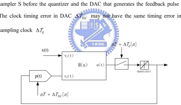
ΣΔ. In such a system, there are two points that require a precise clock signal, the sampler S before the quantizer and the DAC that generates the feedback pulse p(t).
The clock timing error in DAC ΔTDAC may not have the same timing error in the
sampling clock ΔTQ Quantizer1 v1(t) v2(t) H(s) u(t) p(t) x(t) [ ] nT + ΔTDAC n [ ] Q nT + ΔT n
Figure 3.10 Block diagram of a CT ΣΔ modulator including timing uncertainties
We will not consider ΔTQ in our model because it does not contribute
significantly to increase the precision of the predictions and simulations. In general,
DAC timing uncertainties TDAC[ ]n result in a wrong position of the feedback pulses
DAC
T Δ
Figure 3.11 Feedback DACs timing error For a NRZ feedback pulse, the expression of this error area is:
(3.16) We may find the equivalent additive error sequence that produces the same area error in a feedback pulse train with the ideal temporization:
(
)
ΔA n⎣ ⎦⎡ ⎤ = y n⎣ ⎦⎡ ⎤− y n⎡⎣ − 1⎤⎦ ⋅ ΔTDAC ⎡ ⎤⎣ ⎦n[ ] [ ]
(
[ ] [
1]
)
DAC[ ]
j T T A n T n e n Δ = y n −y n− ⋅Δ (3.17)This simple equation (3.17) leads to the model of Fig. 3.12,
Quantizer1 v1(t) v2(t) H(s) u(t) nT x(t) p(t) nT (1-z -1)/T dy(t)
ing an additive jitter model.
ing Fig. 3.13 is the simulation result. In here, the amount of jitter is normalize to clock period and represented in percentages of clock period. For an example, the jitter equals to 1% of clock period at 100MHz sample frequency that also indicates clock jitter equals to 100p.
nj[n]
[ ]
DAC
T n
Δ
Figure 3.12 The Block diagram of a CT ΣΔ modulator includ
By adding this jitter noise model in Matlab/Simulink, we can success to simulate the jitter noise effect the CT ΣΔ modulators. The follow
Figure 3.13 SNDR of the 3rd order modulator with the jitter noise model
Beside the timing non-idealities, there are some other DAC non-idealities, which be mentioned here. The finite DAC response time and consequently no
3.2.5 Further DAC Non-Idealities
n-equal rise nd fall times of the feedback pulse cause a charge mismatch for RZ or even inter symbol interference (ISI) for NRZ pulses. When DAC output current pulses, having unequal rise and fall times, are integrated, the result of the integration depends on the data sequence. This data dependency produces harmonic distortion. As shown in Fig. 3.14, the effect of this feedback waveform asymmetry can be highly attenuated by using a RZ feedback signal.
a
DAC non-linearity is similarly important in CT as in DT modulators, since the low resolution feedback DAC needs linearity as good as the overall modulator. This is due t
3.3 Errors of the Internal Quantizer
The quantizer is located at the most insensitivity. This is why ΣΔ modulators are mostly insensitivity to errors of the internal quantizer, which are usually offset,
hysteresis [42]. None for quantizer timing
issue
as a constant time to settle. o that DAC errors are directly fed into the input of the modulator. Therefore the feedback DAC requires linearity better than the overall modulator. Many techniques have been published to improve the DAC linearity, such as dynamic element matching (DEM) [3, 13] or current calibration [5, 14].
Finite output impedance of the feedback current sources becomes especially important in Gm-C filters realizations. Here, the feedback current steering DAC sees the full filter output swing and thus DAC finite output impedance reduces the linearity.
theless, in CT modulators have to be paid
s. This is caused by timing induced errors like propagation and signal dependent delay:An excess loop delay can be caused by the internal quantizer. More severely, the delay of the decision is dependent on the signal amplitude. A statistically variant quantizer delay causes equivalent performance degradation as clock jitter [43]. This signal dependent delay is easily circumvented by inserting a latch between the quantizer and the feedback DAC. Thus, the quantizer h
Chapter 4
In general, in a CT modulator with enough excess loop delay to push the falling AC pulse edge past a sampling period, the order of the equivalent DT loop is one igher than the order of the CT loop filter. Thus, we use an RZ DAC instead of an
NRZ DAC, the loop gain in CT ld remain the same order as
the loop gain in DT modulators ly what td is, we
could select suitable loop f cients to get exactly the equivalent DT-CT
transform our CT
loop gain matched exactly the desired DT loop gain . It has long been
recognized that it is sensible odulators for excess loop
delay consideration.
edback coefficients, the system is not fully controllable. By adopting a tuning approach where
Analysis on Different Loop Delay
Compensation
The excess loop delay degrades the CT ΣΔ modulators performance in section 3.2.1. There exist some methods to compensate for the excess loop delay. We explore some past proposals and suggest some methods for practical implementations.
4.1 Excess Loop Delay Compensation
D h
modulators G z wouc( )
( )
d
G z for td <0.5. If we knew exact
ilter coeffi
ation. Thus, for a given td <0.5 and RZ DAC pulses, we can make
to use RZ DAC pulses in CT m ( )
c
G z G zd( )
If there exists enough excess delay to push the falling edge of a DAC pulse past a sampling period, it will increase the modulator order by one. Therefore, there will be