(Received July 12, 1999; accepted December 6, 1999)
405
Interfacial Reactions between Liquid Indium
and Au-Deposited Substrates
INTRODUCTION
Soldering has been widely employed in electronic packaging processes where surface mounting tech-nology (SMT), flip chip bonding (FC) and ball grid array (BGA) are concerned. There are many solder alloys used for commercial purposes, among which the PbSn alloys are the most popular on account of their bounteous merits such as wettability, fatigue resistance, corrosion resistance, and, competitive pric-ing. However, adaptation to lead-free solders, out of environmental concerns, has become a top priority in the electronics industry.
Among a slew of lead-free solders developed re-cently,1–3 indium-based alloys have been favored in
bonding devices that demand low soldering tempera-tures.4 Shimizu et al.5 have indicated that
indium-based solders possess excellent mechanical proper-ties, as they display a more endurable fatigue life than PbSn solders in the flip-chip process, and are suitable for the role of high reliability interconnec-tions. Indium has also been added to a number of other lead-free solders in order to increase wettability and lower the melting points.
On the other hand, gold-studs or bumps have also been employed for flip chip attachment. In other flip chip techniques, gold is an important element used as
Y.M. LIU and T.H. CHUANG
National Taiwan University, Institute of Materials Science and Engineering, Taipei, Taiwan, R.O.C.
The morphology and growth kinetics of intermetallic compounds formed during the soldering reactions of liquid indium on Au-deposited substrates in the temperature range of 225°C and 350°C have been investigated. The results show that two types of AuIn2 intermetallic compounds make their appearance: the
continuous-wavy-crystalline type, and the floating-island type. The growth of this intermetallic compound follows the parabolic law, which indicates that the growth is diffusion-controlled. The activation energy of the reaction calculated form the Arrhenius plot of growth reaction constants is 39.42 kJ/mol. Also, the wettability of liquid indium on the surface of the gold-deposited substrate is determined from contact angle measurements. Finally, a mechanism for the interpretation of the wetting behavior of the said Au/In system is proposed, which can be ascertained by SEM observations.
Key words: Gold, indium, soldering, intermetallic compound, activation energy, wettability
the oxidation protective layer in under bump metal-lurgy (UBM) and top surface metalmetal-lurgy (TSM).6 In
addition, the microsoldering of the Au/In/Au layer for electronic contacts has been demonstrated by Mil’shtein et al. as to exhibit good strength,7 and the
thermo-compression bonding of indium with gold bumps has also been adopted for LCD panels.8 In
another microjoining technique known as solid-liquid interdiffusion bonding (SLID, based on the formation of a thin intermetallic compound layer through reac-tions between metallic layers with respectively higher and lower melting points), the Au/In system has also been successfully employed.9 Although the Au/In or
Au/PbIn interfacial reactions have been studied by several researchers, their efforts have targeted pri-marily on solid/solid reactions,10–17 whereas
informa-tion regarding liquid/solid soldering reacinforma-tions is lim-ited thus far.18 In respect of solid-solid-state
reac-tions, Powell and Braun’s investigations10 on the bulk
diffusion of Au/In at temperatures below the melting point of indium showed that four intermetallic com-pounds AuIn2, AuIn, Au7In3, and Au4In were formed,
with AuIn2 as the major layer on the reaction zone. In
their study of thin film diffusion coupling of Au/In, Simic et al.11 showed that the Au and In interdiffusion
took place quickly at room temperature, which re-sulted in the appearance of AuIn2, AuIn, Au7In3, and
Au4In intermetallic compounds. They also pointed
com-Fig. 2. Typical x-ray diffraction pattern of the In/Au interfacial reaction products formed at 350°C for 20 min.
pounds relied much on the Au/In film thickness ratio and diffusion time, and AuIn2 was always the first
phase formed. The study of Au/In thin film reactions by Bjøntegaard et al.12 and Hasumi13 showed that only
the AuIn2 compound was formed by In atoms diffusing
through the preformed AuIn2 to react with Au atoms,
and, from a kinetic point of view, the well-known parabolic law was obeyed. In contrast, Millares et al.14
studied the AuIn2 growth from bulk diffusion couples,
and demonstrated a linear kinetics for AuIn2 layer
growth in short-time reaction, which implied that the reaction was interface controlled. Yost et al.15, 16 have
studied the aging of Au/PbIn solder joints. They found that a thin single-phase layer of Au9In4 and a thick
dual-phase layer of AuIn2 equiaxed grains impeded in
Pb were formed in the aging process. The total reac-tion layer thickness vs. time could be well defined in a linear relationship, which implied that the growth of intermetallic compounds was interface controlled and the activation energy was 0.61 eV. In the solid state reaction of Au/In48Sn, Shohji et al.17 found a
double layer of AuIn2 /Sn-rich γ-phase formed on the
interface between the Au substrate and the In48Sn solder. The AuIn2 layer grew toward the In48Sn
sol-der, showing that the diffusion rate of Au atoms through the AuIn2 layer was much greater than that
of In atoms. The growth of the AuIn2 layer followed the
parabolic law, and the activation energy, which corre-sponded to the activation energy for the diffusion of Au atoms in AuIn2, was 42.8 kJ/mol.
In contrast to plentiful investigations on Au/In solid state reactions, those on liquid/solid reaction are seldom. Jacobson18 indicated that Au formed a
con-tinuous layer-type interfacial compound of AuIn2 with
In when heated above the melting point of In. Once formed, this AuIn2 layer would act as an effective
dissolution barrier for Au to dissolve into the In solder. However, no detailed kinetic data have been available thenceforth.
In this present study, the morphology of the inter-facial compounds and kinetics of the soldering reac-tion of liquid In and solid Au deposited Al2O3 substrates
have been investigated. In addition, since the knowl-edge of wetting behavior of the In solder on Au sub-strates is essential to their applications, the wettability of liquid indium on gold substrates is also evaluated.
EXPERIMENTAL
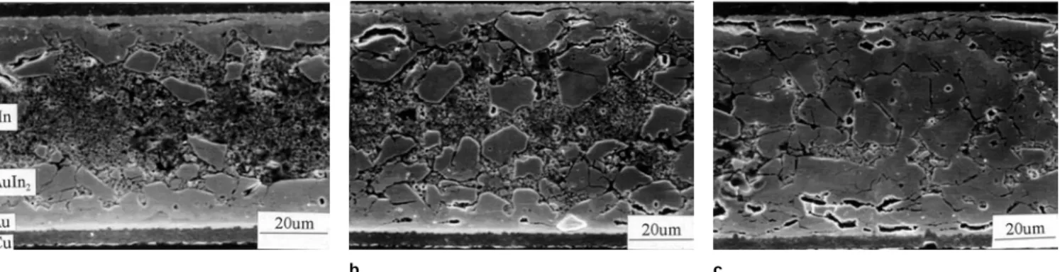
The Au layer with a thickness of 6 µm was deposited on an Al2O3 substrate by sputtering. For the improve-Fig. 1. Morphology of intermetallic compounds formed during interfacial reaction between In and Au at 300°C for (a) 5 min, (b) 15 min, (c) 20 min.
a b c
Table I. Chemical Composition of the Intermetallic Compounds Formed in the Interfacial Reaction
Temp. I.P. Phase I.M. Position Au (at.%) In (at.%) Cu (at.%)
225°C AuIn2 (Cu) Continuous Layer 30.0 69.6 0.4
25 min Floating Island 30.5 69.2 03.3
250°C AuIn2 (Cu) Continuous Layer 32.4 65.6 2.0
25 min Floating Island 31.6 66.8 1.6
300°C AuIn2 (Cu) Continuous Layer 30.8 66.2 3.0
25 min Floating Island 30.6 66.8 2.6
325°C AuIn2 (Cu) Continuous Layer 29.3 64.7 6
ment of adhesion between Au and Al2O3, a Cu
interlayer with a thickness of 4 µm was employed. Specimens of a size of 8 mm × 8 mm were cut from the substrates and then ultrasonically degreased in ac-etone. The indium solder was rolled from an In ingot with 99.99% purity into a 0.2 mm-thick foil. The foil was cut to the same size as the Au-deposited substrate. For testing the soldering reaction, an In foil was inserted between two Au-deposited substrates. The sandwiched sample was heated in an IR furnace under a vacuum of 10–3 torr. Soldering was conducted
between 225°C and 350°C from 5 to 30 min. The sample was then cooled down to room temperature in 2 min by water cycling as pertained to the heating stage.
The soldered specimens were cut along the cross-section, ground with SiC paper, polished with 1 and 0.3 µm Al2O3 powders and deposited with carbon in
the vacuum evaporator to avoid the charging phe-nomenon of the Al2O3 substrate in SEM or EPMA.
Morphology observations were mostly conducted through applying a scanning electron microscope (SEM). Intermetallic compounds were identified with electron probe micro analyzer (EPMA) and x-ray diffractometer (XRD). To prepare for the XRD
analy-Fig. 3. Migration of In(l)/Au(s) interface toward the Au substrate after
soldering reaction at 250°C for 10 min. (The original interface was marked with a Cr thin film.)
a b
Fig. 4. Appearance of granular intermetallic compounds formed during In/Au interfacial reactions. (a) 300°C, 10 min; (b) 300°C, 20 min.
sis, the chosen specimens were selectively etched with a solution of 10 ml HF, 10 ml H2O2 and 40 ml H2O,
so that the In solder would dissolve and the interme-tallic compounds would remain. As the formation mechanism of intermetallic compounds in the solder-ing reaction ought to be clarified, certain Au-depos-ited Al2O3 substrates were sectionally marked by
sput-tering-deposition of a Cr thin film. From the phase diagram, it could be observed that Cr would not react with In, and the deposition of a Cr thin film on an Au substrate worked as a diffusion barrier at the In(l)/
Au(s) interface. Thus, the original In(l)/Au(s) interface
could be identified.
The wettability of liquid indium on Au-deposited substrates was evaluated by measuring the contact angles of the indium sessile drop on the Au-deposited Al2O3 substrate at the temperatures of the soldering
reaction. The measurement was carried out by plac-ing an indium cylinder of 2 mm in diameter and 2 mm in height on an Au-deposited Al2O3 substrate in an IR
furnace under a 10–3 torr vacuum. Prior to measuring,
the indium cylinders were dipped with a mildly acti-vated rosin flux. During the heating process, the variation of the contact angles with time was recorded by an in-situ video system.
RESULTS AND DISCUSSION
The morphology of the Au/In/Au joint after solder-ing reactions at 300°C for various lengths of time was shown in Fig. 1. Two main types of intermetallic compounds turned out during the soldering process: the continuous wavy type on the Au/In interface and the floating-island type in the interior matrix of the indium solder. Both types of intermetallic compounds grew with the increase of reaction time and soldering temperature. The compositions of both intermetallic compounds were analyzed by EPMA and shown in Table I. These results were averaged from the data taken from at least five spots of the intermetallic compounds. It revealed that both types of intermetal-lic compounds possessed a similar composition of the AuIn2 phase. The x-ray diffraction pattern shown in
formed in the soldering reaction was of the AuIn2 phase.
In a study on the solid-liquid reaction of Cu/Sn, Ni/ Bi and Cu/In systems, Kao19 showed that the rapid
dissolution of substrate atoms into the liquid solder would form an irregular structure of interfacial inter-metallic compounds. On the other hand, the reaction between a substrate and a solder saturated with the substrate metal, as the dissolution would be inhibited in this case, would produce a more regular intermedi-ate layer structure. Consistent with Kao’s findings, the irregular shape of AuIn2 compounds formed at the
Au/In interface in the current study should also be attributed to the rapid dissolution of Au into the In solder. Such a mechanism could be reaffirmed by referencing the study of Tu et al.,20 in which they
indicated that the fast dissolution of Au in the PbSn alloy, pure Sn, Sn4Ag and Sn20In2.8Ag alloys would incur a sunken curvature in the reaction interface, as well as intermetallic compounds precipitating in the solder matrix while cooling. In this present study, through sputtering a Cr thin film on the partial surface of the Au substrate to function as a diffusion marker for the Au(s)/In(l) soldering reaction, the Au(s)/
In(l) interface was found to migrate toward the Au
substrate and form a sunken curvature in the area adjacent to the Cr marker (Fig. 3). In addition, the appearance of floating-island-type intermetallic com-pounds in the In solder matrix (as shown in Fig. 1) also confirmed the results of Tu et al.20
Through selectively etching the remaining indium solder on the polished surface of the specimens, it was found (as shown in Fig. 4) that the continuous wavy type of intermetallic compounds was a layer of equiaxed grains grown from the Au/In interface into the indium solder matrix. A similar appearance of granular intermetallic compounds on the interface has also been observed by Yost et al. in their study of the interfacial reaction of the Au/PbIn system.15 It
was also found in the current study that during the reaction, the granular intermetallic compounds grew in size while decreasing in number (see Fig. 4a and b). This implied that a ripening effect occurred accompa-nying the growth of intermetallic compounds.
Since Au manifested no solubility in solid In, the floating-island type of intermetallic compounds in the indium solder should result from Au atoms dissolving in liquid indium during the soldering reaction, and then starting to precipitate after cooling down from the soldering temperature. However, as the reaction time was stepped up, some of the intermetallic com-pounds in the continuous wavy layer would split away from the interface and float into the indium solder to form more island-type intermetallic compounds in the solder matrix.
As Table I delineated, the concentration of the dissolved Cu in the AuIn2 phase would rise with the
increase of soldering temperature and time. The rea-son for the Cu impurity existing in the AuIn2 phase
could be traced to the outward diffusion of the Cu adhesive layer between Au and the Al2O3 substrate.
During the soldering reaction between liquid In and
the solid Au layer, solid-solid interdiffusion between Au and Cu layers occurred simultaneously. However, the reaction rate of the latter, in contrast to that of the former, was too slow to bring about the accumulation of Cu at the In/Au interface above the saturated limit so as to form the CuxIny intermetallic compound. As a Fig. 5. Simultaneous interfacial reaction of In(l)/Au(s) and In(l)/Cu(s) at
350°C for 20 min to form the Cu11In9 intermetallic compounds (black
particles) and AuIn2 intermetallic compounds (gray lumps).
Fig. 6. The thickness of AuIn2 intermetallic compound related to the
square root of time for the Au/In interfacial reaction.
Table II. The Logarithmic Exponents and Growth Constants of Intermetallic Compounds Formed
during the Au/In Interfacial Reactions
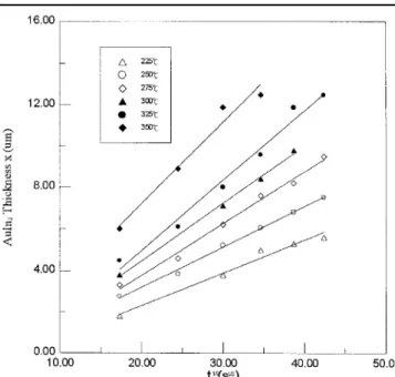
T (°C) Kp (cm2/sec) 225 1.96 × 10⁻¹⁰ 250 3.32 × 10⁻¹⁰ 275 5.28 × 10⁻¹⁰ 300 6.70 × 10⁻¹⁰ 325 9.73 × 10⁻¹⁰ 350 1.41 × 10⁻⁹
result, the outwardly diffusing Cu atoms continued to dissolve into the AuIn2 phase. With the increasing of
soldering temperature and time, the outward diffu-sion of Cu atoms accelerated accordingly, resulting in a hike of the Cu content in the AuIn2 phase. Not until
undergoing a prolonged reaction at a relatively higher temperature, did the Au layer reach a nearly exhausted state, enabling a sufficient amount of Cu atoms to react with the In solder. Then, a few of the granular Cu11In9
compounds began to form, which were embedded in the AuIn2 particles as shown in Fig. 5.
The measured growth thickness of interfacial AuIn2
intermetallic compounds (∆x) corresponding to the square root of the reaction time (t1/2) was plotted in
Fig. 6, which revealed a linear relation. The devia-tions of measurements were between 0.2 µm and 1.3 µm. It indicated that the kinetics of the Au/In interfacial reaction obeyed the parabolic law and the growth of intermetallic compounds was diffusion-controlled. This result was consistent with Jacobson’s study on Au/In soldering reactions that the interfacial dissolution would be retarded at the formation of the interfacial AuIn2 layer.18 The reaction constants Kp,
defined as Kp = ∆x2/t and prescribed for various
soldering temperatures, were given in Table II. The Arrhenius plot of Kp was shown in Fig. 7, where the activation energy Q of the intermetallic compound growth was calculated to be 39.42 kJ/mol. The activa-tion energy here was very close to 42.8 kJ/mol for Au diffusion through the AuIn2 layer into the InSn layer
in the Au/InSn reaction, as reported by Shohji.17
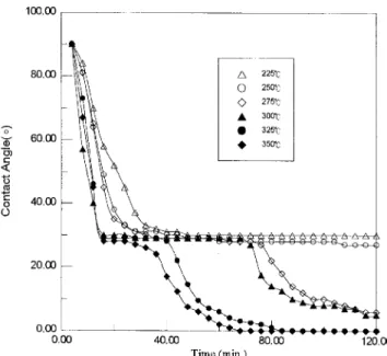
To evaluate the wettability of liquid indium on Au-deposited substrates, the contact angles were mea-sured by the sessile drop method at various tempera-tures. The values were plotted as a function of reac-tion time in Fig. 8. It was found that the contact angles of all specimens declined rapidly to about 30° as the indium cylinders began to melt, and then the curves
Fig. 7. Arrhenius plot of the growth rate constants (Kp) for the Au/In interfacial reaction.
Fig. 8. Plots of contact angles for liquid indium sessile drop wetting on Au deposited substrate versus reaction time at various temperatures.
remained as a plateau for a period of time before they finally collapsed to a very low value. Wang et al.21,22
also experienced a similar process in their study on the wetting of the PbSn alloy on Cu and Ag substrates. With respect to wetting of the metal surface by liquid solders, which could usually be ascribed to a reacting system, the solder droplets were sometimes observed with halos or precursor films leading the contact line spreading.23 For example, Kim et al.’s study on the
a
b
c
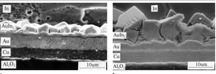
Fig. 9. Schematic presentation of the mechanism of the wetting be-havior of indium solder on the Au-deposited substrate: (a) quasi-wetting stage, (b) formation of precursor halo, and (c) final wetting stage.
wetting of the eutectic PbSn solder on a Cu substrate showed that after the initial spread, the wetting angle remained constant, and the reaction carried on through the formation of intermetallic compounds at the Cu/ PbSn interface and the appearance of a band side (halo) surrounding the solder edge.24 Yost et al. have
proposed that the intermetallic compound formation at the interface should exert a more significant influ-ence on the wetting than the driving force of imbal-ance of the surface tensions in a soldering reaction system.25 In view of observations made by Wang et
al.21,22 and Kim et al.,24 and the driving force theory
proposed by Yost et al.,25 a mechanism for the wetting
of the In solder on Au-deposited substrates is pro-pounded in this study, as schematized in Fig. 9.
The indium solder melt at the initial stage and resulted in a quasi-wetting contact angle θ1 (Fig. 9a).
Accompanying the formation of intermetallic com-pounds at the In/Au interface, some indium atoms spread out of the solder drop through free surface diffusion on Au-deposited substrates. As these out-spreading indium atoms could diffuse farther away from the edge of the liquid drop and accumulate to a critical thickness, reaction with the Au surface would occur, and a precursor halo would thereby appear (Fig. 9b). The formation of intermetallic precursor halos caused the surface tension of the vapor/sub-strate ahead of the indium solder drop to vary from
γv/Au to γγv/I.M.. Also, the surface tension of the solder/
substrate interface would change from γIn/Au to γIn/I.M..
The change of surface tensions resulted in the drastic decrease of the contact angle to θ2 (Fig. 9c). This
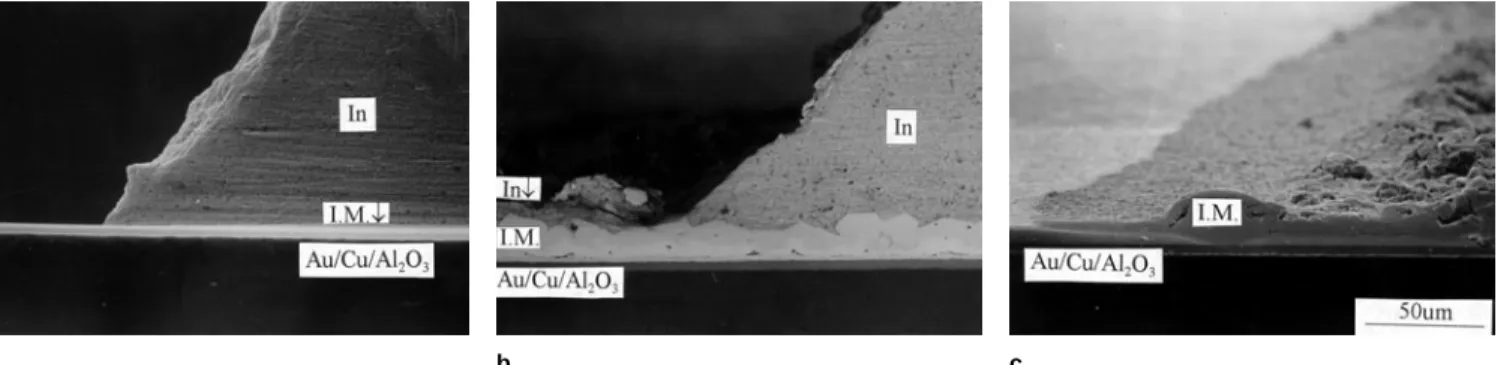
mechanism was brought to light through SEM obser-vations of the cross-sections of specimens after wet-ting tests, as shown in Fig. 10, where three stages of the wetting process corresponding to those described above in the proposed mechanism (Fig. 9a, b, and c) were clearly delineated.
CONCLUSIONS
In the soldering process of liquid indium with Au-deposited substrates in the temperature range of 225°C to 350°C, the intermetallic compound AuIn2 is
found to appear in two continuous wavy and floating-island forms. The growth kinetics of AuIn2 follows the
parabolic law, which indicates that the reaction is diffusion-controlled and the activation energy is
39.42 kJ/Mole. The wetting tests in the temperature range between 225°C to 375°C show that the contact angle of liquid indium on Au-deposited substrates declines rapidly to about 30° at the initial stage, and then remains constant for a period of time before finally collapsing to a very low value. For the interpretation of such a wetting behavior, a mechanism has been pro-posed, which is based on the formation of precursor halos ahead of the liquid indium drop. Through SEM observations of the cross-sections of the specimens after wetting tests, three stages of the wetting process in the proposed mechanism can be clearly ascertained.
Fig. 10. SEM observations of the wetting behavior of indium solder on the Au-deposited substrate: (a) quasi-wetting stage, 300°, 3 min; (b) formation of precursor halo, 300°C, 45 min; and (c) final wetting stage, 300°C, 120 min.
a b c
REFERENCES 1. S.K. Kang, J. Electron. Mater. 23, 701 (1994). 2. J. Glazer, Int. Mater. Rev. 40, 65 (1995).
3. T. Laine-Ylijoki, H. Steen, and A. Forsten, IEEE Trans.
Comp., Pac. Man. Tech. 20, 194 (1997).
4. J. Glazer, J. Electron. Mater. 23, 693 (1994).
5. K. Shimizu, T. Nakanishi, K. Karasawa, K. Hashimoto, and K. Niwa, J. Electron. Mater. 24, 39 (1996).
6. R.R. Tummala, E.J. Rymaszewski, and A.G. Klopfenstein,
Microelectronics Packaging Handbook (New York: Chapman
& Hall, 1997).
7. S.K. Mil’shtein, J.M. Parsey, Jr., D.V. Lang, D.C. Joy, and H. Temkin, IEEE Trans. Comp., Pac. Man. Tech. 8, 397 (1985). 8. M. Mori, M. Saito, A. Hongu, A. Niitsuma, and H. Ohdaira,
IEEE Trans. Comp., Pac. Man. Tech. 13, 444 (1992).
9. C.C. Lee, C.Y. Wang, and G. Matijasevic, J. Electron. Pac. 115, 201 (1993).
10. G.W. Powell and J.D. Braun, Trans. AIME 230, 694 (1964). 11. V. Simic and Z. Marinkovic, Thin Solid Films 41, 57 (1977). 12. J. Bjøntegaard, L. Buene, T. Finstad, O. Lonsjo, and T. Olsen,
Thin Solid Films 101, 253 (1983).
13. Y. Husumi, J. Appl. Phys. 58, 308 (1985).
14. M. Milliares, B. Pieraggi, and E. Lelievre, Scrip. Metal.
Mater. 27, 1777 (1992).
15. F.G. Yost, F.P. Ganyard, and M.M. Karnowsky, Metal. Trans. 7A 1141 (1976).
16. F.G. Yost, Gold Bull. 10, 94 (1977).
17. I. Shohji, S. Fujiwara, S. Kiyono, and K.F. Kobayashi, Scrip.
Mater. 40, 815 (1999).
18. D.M. Jacobson and G. Humpston, Gold Bull. 22, 9 (1989). 19. C.R. Kao, Mater. Sci. Eng. A238, 196 (1997).
20. P.G. Kim and K.N. Tu, Mater. Chem. Phys. 53, 165 (1998). 21. X.H. Wang and H. Conrad, Scrip. Metal. Mater. 30, 725 (1994). 22. X.H. Wang and H. Conrad, Scrip. Metal. Mater. 31, 375 (1994). 23. F.G. Yost, F.M. Hosking, and D.R. Frear, The Mechanics of
Solder Alloy Wetting and Spreading (New York: Van Nostrand
Reinhold, 1993).
24. H.K. Kim, H.K. Liou, and K.N. Tu, J. Mater. Res. 10, 497 (1985).
25. F.G. Yost and A.D. Romig, Jr., Mater. Res. Soc. Symp. Proc. 108, 385 (1988).