Parasitic-capacitance-insensitive current-mode
filters using operational transresistance amplifiers
J.-J. Chen H.-W. Tsao S.4. Liu W. Chiu
Indexing terms: Biquadfilters, Current-modejilters, MOSFET-C integrator, Parasitic capacitances
Abstract: Aparasitic-capacitance-insensitive MOS- FET-C integrator and differentiator using oper- ational transresistance amplifiers are proposed and experimental results demonstrated. The band- widths of these circuits are also independent of their gains. The required capacitances are smaller than those in previous work. Two new configu- rations of universal current-mode biquad filters based on these circuits are presented. A second- order bandpass filter constructed using universal biquad filters and another third-order Chebyshev lowpass filter with 0.1 dB passband ripple are breadboarded and the measured results presented.
1 Introduction
The continuous-time filter techniques have been receiving considerable attention in MOS VLSI technology because the characteristics of these filters can be stabilised against fabrication tolerances and temperature variations [Z]. In certain applications it has been demonstrated that continuous-time filters offer advantages over other types of IC filter, such as switched-capacitor and digital filters [2]. Also, it is well known that the bandwidth of a tradi- tional operational amplifier depends on the closed-loop voltage gain. The attempt to overcome this problem has led to renewed interest in circuits that operate in the current mode [l-41. Circuits using current-processing techniques have improved dynamic capability and a par- ticular feature of these designs is their ability to provide a constant bandwidth that is virtually independent of the closed-loop gain. In this paper, we use an amplifier termed an operational transresistance amplifier (OTRA) to implement a current-mode integrator and differentia- tor. Since the OTRA has one output terminal with low impedance and two input terminals that are virtually grounded, most effects of parasitic capacitances disap- pears and the remainder can be compensated without adding any extra components. Also, since the input ter- minals of these circuits are virtually grounded, they are cascadable. To verify the functions of our proposed cir- cuits, experiments on these circuits have been carried out and the resulting measurements are presented.
0 IEE, 1995
Paper 195OG (EIO), first received 18th May 1994 and in revised form 13th March 1995
The authors are with the Department of Electrical Engineering, Na- tional Taiwan University, Taipei, Taiwan, 10764, Republic of China 186
2 Circuit descriptions
The circuit symbol and a practical circuit of the OTRA are described in Fig. la and b, whose terminal character- istics can be described as [SI
Obviously both input terminals of an OTRA are virtually grounded and the output voltage is the difference of two input currents multiplied by transimpedance Z J Z , ( Z , is
V. V-
K s
one-output current mirror two-output current mirror
9
0Fig. 1 Operational transresistance ampl$er
LI Symbol
h Circuit
the total effective output impedance of the two-output current mirrors and Z L is the external load impedance). In most applications the operational transresistance
amplifiers together with passive networks can be employed to construct signal-processing circuits. Negat- ive feedback through passive elements forces the currents I , and I , to be equal whenever the magnitude of ZJZ, approaches infinity. Therefore if suitable passive net- works are selected, many useful transfer functions can be realised.
The channel current id of the MOSFET biased in the triode region can be expressed as [2]
id = F(u,, VG) - F(us, VG) (2) where F(U, VG) = 2 K ( VG - V, - V,, -
4 p ) U
- K(u - V,), - $Ky(u - V,+
4p)3’2
W K = K c o xW and L are the channel width and length, respectively, ps is the effective channel mobility, V,, is the flatband voltage, N , is the substrate doping concentration, CO, is the oxide capacitance per unit area,
4,
is the approx- imate surface potential at strong inversion, V, and V, are the gate and substrate voltages, respectively.We use a capacitor, an OTRA and two MOSFETs to realise the MOSFET-C integrator and differentiator. The proposed MOSFET-C integrator and differentiator are shown in Figs. 2 and 3. The relationship between the
-
I I
Proposed integrator bosed on single O T R A Fig. 2 “GB
P
-4
12=E+-
-b
VGAFig. 3 Proposed diflerentiotor based on single O T R A
output currents I , , I4 and input currents I , , I , of the integrator is
13(s) - I&) = ~ K ( V G A -
VGE)V,(S)
or
(4)
To analyse the frequency-domain characteristics of this integrator Z,(s) can be represented as N ( s ) / D ( s ) and all roots of both polynomials N ( s ) and D(s) are located in the left half of the s-plane. Eqn. 4 can therefore be rewritten as
( 6 ) Since the capacitance C is fixed and the current gain of this integrator can be varied by adjusting the voltage dif- ference V,, - V,,, the poles and zeros of the proposed integrator are always fixed. Thus the bandwidth of the MOSFET-C integrator is nearly constant and independ- ent of the current gain.
In a similar way the current tranfer function of the MOSFET-C differentiator can be derived as
1 3 ( s ) - 14(s) - 2K(VG.4 - V G B ) N ( s )
I , ( s ) - 12(s) - sCN(s)
+
D(s)This MOSFET-C differentiator also has a bandwidth independent of the current gain as long as the voltage difference VGA - V,, is kept constant.
We then use the proposed inegrator and differentiator to implement some configurations of universal biquad filters and higher-order filters. The transfer function of the universal biquad filter shown as Fig. 4 can be
P I
!
I
‘ b A q
%
Fig. 4 A , = vG”l,... B , = VOB1, ... obtained asUniuersnl biquadfilrer using the integrators shown in Fig. 2
I E E Proc.-Circuits Devices Syst., Vol. 142, N o . 3, June 1995
(9) 187
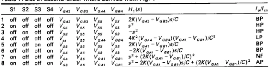
T a b l e 1 : L i s t o f s e c o n d - o r d e r f i l t e r s d e r i v e d f r o m Fig. 4 s1 s 2 s3 5 4 VGA3 v,,, Vo*n VG,, H l ( 5 - ) I O / l # " 1 off off 2 on off 3 off on 4 off off 5 off off 6 off off 7 on off 8 on off V , = most NF = notch
the numerator H,(s) of the transfer function is dependent on the connection patterns of the switches shown in Fig. 4. For example, if a bandpass filtering function is required the switches and gate voltages of MOSFETs shown in Fig. 4 must be connected as described in the first row of Table 1. All of the switches must be turned off, the gate voltages V,,, and V,,, is used to bias the MOSFETs in the triode region, and the MOSFETs with gate voltage V,, will operate in the cutoff region. The other possible options, which can yield useful second- order filtering functions, are also summarised in Table 1. The centre frequency 0, and quality factor Q of this uni-
versal biquad filter can be derived as
The transfer function of the differentiator-based universal biquad filter shown in Fig. 5 can be expressed as
BP H P HP LP BP BP NF AP filter;
-
10 f Fig. 5 A , = V,",, ... E , = V,,,, . . .Universal biquadfilter using the differentiators shown in Fig. 3
are listed in Table 2. Furthermore, using the leapfrog syn- thesis method, a third-order lowpass Chebychev filter shown in Fig. 6 can also be obtained.
(12) with (14) C c2 Q='
where HZ(s) also depends on the connection patterns of switches and MOSFETs. The useful second-order filter- ing functions that can be realised with this biquad filter
Fig. 6
in Fig. 2
A = V , , B = V,,
Third-order Chebyshev lowpass filter using integrators shown
3 Effects of parasitic capacitances
To investigate the effects of parasitic capacitance in the proposed integrator, we redraw this integrator including
188
T a b l e 2 : L i s t o f s e c o n d - o r d e r f i l t e r s d e r i v e d f r o m Fig. 5
s1 s 2 s3 s 4 VGA2 v G 8 2 v G I S ' , E 3 H 2 ( s ) /Ji"
BP 1 Off Off Off Off VGm VGm v s s v s s 2K(V,Az-VG&/C,
2 on off off off V,, V,, Vss V,, s2 HP
3 off on off off V,, V,, V,, V,, -5' HP
5 off off on off V,, V,, V,, V,, 2 K ( V G A , - V,,,)s/C, BP BP
6 off off off on V,, V,, V,, V,, -2K(VG,, - V,,,)s/C,
7 on off off off V,, Vss V,,, V G B , s 2 + 4 K 2 ( V G A 1 - V G E , ) / C ? N P
8 on off off on V,, V,, V,,, V,,, sz - 2K(VG,, - V G , , ) s / C , +4K2(V,,, - V G E , ) / c ? AP V,, = most negative power supply; HP = highpass filter; BP = bandpass filter; LP = lowpass filter; NF = notch filter; AP = allpass filter
4 Off Off Off off VSS VSS V G A ~ V G B J 4K2(Vc,7 - v c ~ ? ) ( v G ~ 3 - v G ~ 3 ) / c ? LP
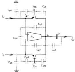
parasitic capacitances as shown in Fig. 7. Due to the vir- tually grounded input and low-impedance output charac- teristics of an OTRA, capacitances C P 9 , C p l o and C , , ,
Fig. 7 : c m 3 ... . . . . , . , . ., CP2
:
C m nProposed integrator with all parasitic capacitances
1
: : C P '1
... ,.
..._. .I . . . . , ... I . . ... , . , . 'j1
! c
1
: : : P2 CP3 - -Fig. 8 Proposed differentiator with all parasitic capacitances
have little effect. Next, since the voltage sources V,, and V,, are DC, the effect of C p 5 , C p 6 , C,, and C,, will also be negligible. Then the voltage V, can be obtained as
The relationship between the input and output currents I , , I , , I , and I 4 is
I&) - I&)
= ( W V G A - VGE)
+
s(C,i - CP2))V,(s) (16)x (Il(4 - 12(s)) (1 7)
The capacitances C,, and C p 2 are drain-to-source capa- citances of the two NMOS transistors in Fig. 7. Since the aspect ratios and drain-to-source voltages of both NMOS transistors are identical, capacitances C,, and Cp2 are approximately equal. With
I
Z,(s)I
approaching IEE Proc.-Circuits Devices Syst., Vol. 142, N o . 3, June 1995infinity, the current gain function is simplified to
The gain tolerance of this integrator caused by capa- citances C,, and C,, can be compensated through adjusting the voltages V,, and V,, or the use of some predistortion technique without adding any extra com- ponents.
The proposed differentiator with parasitic capacitances is shown in Fig. 8. For similar reasons, the capacitances C,, , C , , , C,, , C,, , C p 8 , CP9 and Cplo have negligible effect, and the resultant current transfer function of the differentiator can be expressed as
This circuit can also be compensated by adjusting V,, and V,, or through the use of some predistortion tech- nique without additional devices.
If the layouts of all integrators and differentiators are similar, the gain tolerances are nearly equal and the required compensating adjustments of voltages V,, and V,, are also identical. This is convenient when consider- ing the compensation aspects of circuit design.
4 Harmonic distortion analysis
Using the level-3 MOSFET model of SPICE, the dependence of the mobility on VGs and the threshold voltage on V,,, can be derived as [6,
71
VTH = VFB
+
24, - U ~ D S+
YF,J(Z+p - VES)+
F"(24, - VES) (21)F, and F , are the parameters of short-channel and narrow-width MOSFETs. Analysis results (Section 8.1) show that only second-order harmonics exist in the pro- posed integrator and the total harmonic distortion can be expressed as
T H D 5 HD,
where I , - , is the peak-to-peak amplitude of the input current. The total harmonic distortion of the proposed differentiator has also been derived and is given in Section 8.2.
5 Experimental results
We use the circuit shown in Fig. 9 to implement an OTRA. The commercial IC AD844AN and CA3600E are 189
employed to construct all the experimental circuits. To investigate the effect of parasitic capacitances, the pro- posed integrator with parasitic capacitances shown in
v.
Fig. 9 O T R A constructed with current feedback op-amps
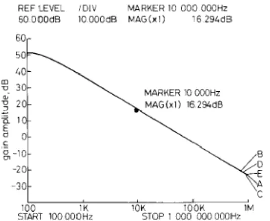
Fig. 7 is breadboarded. We have added external capa- citors to simulate parasitic capacitances C,,,, C,, , C,, and C,, and selected all 'parasitic' capacitances to be 1 nF. The measured gain and phase response of our inte- grator without and with parasitic capacitors is shown in Figs. 10 and 11, respectively. Curves A-E are the meas-
REF LEVEL i D l V MARKER IO 000 OOOHz 60000dB 10OOOdB MAG(x1) 16 294dB 60- MARKER 10 OOOHz G g - 1 0 - -20- -30- I 100 1K 10K IOOK IM
START 100 OOOHr STOP ! 000 000 OOOHz Fig. 10 Comparisons between measured gain responses of proposed integrators with and without adding capacitors to simulate 'parasitic' capacitances
REF LEVEL iDlV MAKER 9 794 328Hz OOdeg 45 OOOdeg PHASE(x1) -89707deg
i
$ 1
0; 0" MARKER 9 794 328HZ 135"I
100 1K 10K lOOK IMSTART 100 OOOHz STOP 1 000 000OOOHz Fig. 11 Comparisons between measured phase responses of proposed integrators with and without adding capacitors to simulate 'parasitic' capacitances
ured results of the proposed integrator, with no 'parasitic' capacitor and one of C , , , , C,,, C,, and C,, included one at a time, respectively. The maximum gain difference is seen to be only 0.4 dB.
190
The second-order bandpass filter derived from Fig. 4 is breadboarded and its experimental results are given in Fig. 12. To obtain a bandpass filtering function
REF LEVEL l D l V MARKER 91 259 357Hz 6 OOOdB 4000dB MAG(D2) 1 989dB 0 Odeg 45 OOOdeg MARKER 91 259 357Hz
PHASE(D2) 0 175deg I
'-
-2 - MARKER91 259 357Hz MAG (D2) 1 989dB m U 2 -10- -30 PHASE (D2) 0 175 deg I / IIO0 1K !OK IOOK IM
START 100 OOOHz STOP 2 000 000 OOOHz Fig. 12
derivedfrom Fig. 4
Measured amplitude and phase responses of bandpass filter
with centre frequency at 91.3 kHz and quality factor Q = I, we turned off all switches shown in Fig. 4 and
set V,,,.= V,,, =
V,,, = 5.4 V, V,,, = V,,, = V,, and all capacitors to be 2 nF. The gain of the bandpass filter at centre frequency is 1.98 dB, which is greater than the theoretical value (0 dB). This gain tolerance is caused mainly by the mis- match of MOSFETs. All of the filters summarised in Tables 1 and 2 are tunable by varying the gate voltages of NMOS transistors.
The third-order Chebyshev lowpass filter with 0.1 dB passband ripple as shown in Fig. 6 is also tested. The bandwidth of this lowpass filter is about 190 kHz. The capacitor values chosen are C, = 1.43 nF, Cz = 1.59 nF, C, = 1.43 nF and V,, = 8.6 V, VcB = 5.9 V. The experi- mental results of the gain and phase responses are shown in Fig. 13. To verify the theoretical results of harmonic
V,,, = V,,, = V,,, = 7.6 V,
REF LEVEL /DlV MARKER 91 259 357Hr
0 dea 90 OOOdB MARKER I 002 374Hz 0 OOOdB 5 0 0 0 d B MAG(D3) -5 938dB PHASE(D3) 6 926deg 0 MARKER 1 002 374Hz
.r
MAG(D3) -5 938dBI
-10- m -15- ai -20- U MARKER 1 002 374Hz a -40 - -45 -50 - 10K lOOK IMSTOP 2 OOO 000 OOOHz 1K
START 200 OOOHr
Fig. 13 Measured amplitude and phase responses of third-order Chebysheu lowpassfilter shown in F l g . 6
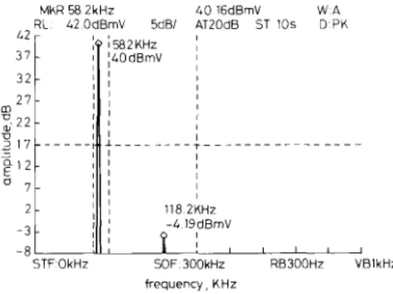
distortions, the harmonic components in the output of the proposed integrator have also been measured. We select I , - I , = 500 cos ( 2 ~ 6 0 x 103t)pA and sense the I E E Proc.-Circuits Devices Syst., Vol. 142, N o . 3, June 1995
output current I , - I , using a 10 kQ resistor; the output
of the integrator is then measured and shown in Fig. 14. Obviously, only the second-order harmonic component is
2 - - 3
-a
MKR 58 ZkHz 40 16dBmV W A RL 420dBrnV 5dBi ATZOdB ST 10s D PK 1 ; 118 2KHz1 ;
-4 19dBrnV -I ;
9 1 L l I I l
10 ALLEN, P.E., and HOLBERG, D.R.: ‘CMOS analog circuit design’. HRW, Inc., Orlando, FL, 1987
11 TAKAGI, S., FUJII, N., and YANAGGISAWA, T.: ‘A canonical continuous-time MOSFET-capacitor filter with high linearity’. Pro- ceedings of IEEE international symposium on Circuits and systems,
12 ALLEN, P.E., and TERRY, M.B.: ‘The use of current amplifiers for high performance voltage applications’. IEEE J . Solid State Circuits.
1980,17, pp. 155-162 1988, pp. 2177-2180
3 2 t
il
I
Ifrequency, KHz
Fig. 14 Spectrum analyser display of harmonic components at output of proposed integrator with V , , = 7.9 V and V,, = 6.9 V ; only second- order harmonic components at 118.2 kHz is observable
detectable and is 44dB lower than the fundamental signal.
6 Conclusion
New parasitic-capacitance-insensitive current-mode filters using operational transresistance amplifiers have been proposed. Since the OTRA has virtually grounded inputs and low impedance output, most effects of the parasitic capacitances disappear and the remainder can be easily compensated without adding any extra ele- ments. All the proposed circuits are cascadable and have almost contant bandwidths, thanks to the low input impedance and the use of current feedback. These filters are also tunable by varying the gate voltages of the MOS transistors and are therefore suitable in many signal pro- cessing applications.
7 References
I CZARNUL, Z.: ‘Novel MOS resistive circuit for synthesis of fully integrated continuous-time filters’, IEEE Trans., 1986, CAS-33, pp. 718-721
2 BANU, M., and TSIVIDIS, Y.: ‘Continuous-time MOSFET-C filters in VLSI’, IEEE Trans., 1986, CAS-33, pp. 125-139 3 SEDRA, A., and SMITH, K.C.: ‘A second generation current con-
veyor and its applications’, IEEE Trans., 1970, CT-17, pp. 132-134 4 TOUMAZOU, C., LIDGEY, F.J., and HAIGH, D.G. (Eds.): ‘Ana-
logue IC design: the current-mode approach’ (Peter Peregrinus, 1990)
5 CHEN, J.J., TSAO, H.W., and CHEN, C.C.: ‘Operational trans- resistance amplifier using CMOS technology’, Electron. Lett., 1992,
28, (22), pp. 2087-2088
6 ANTOGNEITI, P., and MASSOBRIO, G.: ‘Semiconductor device modelling with Spice’ (McGraw-Hill, Singapore, 1988), pp, 184-207 7 HSPICE User’s Manual, version H92. Meta-Software, Inc.
8 ISMAIL, M., SMITH, S.V., and BEALE, R.G.: ‘A new MOSFET-C universal filter structure for VLSI’, IEEE J . Solid State Circuits,
1988,23, pp. 183-194
9 TOUMAZOU, C., LIDGEY, F.J., and CHEUNG, P.Y.K.: ‘Current-mode analogue signal processing circuits - A overview 01
recent developments’. Proceedings of IEEE international sympos- ium on Circuits and systems, 1980, pp. 1572-1575
IEE Proc.-Circuits Devices Sysl., Vol. 142, No. 3, June 1995
8 Appendix
8.1 Analysis of harmonic distortions in proposed
integrator
The difference of the output currents I , and I , as shown in Fig. 2 can be obtained as
with O(Vcs
-
Ifr,,) 9 1 (23)If i , - i2 = I , - ? cos ut and
I
Z,(jo)I
approaches infinity, the voltage U, will be= -
U s ) }
I -.
w c - - JLI sin wt Since I? . Y - ’{ { V,(s)*
V J s ) } } = (u,(t))’ = sin’ wt ( 2 5 ) i&) - i4(t) 1+
F E sinz cotVCA
+
VcE I p - p sin cot w c+
F n ( 2 4 p - vES) --))
2Obviously, only the second-order harmonic component is present and the total harmonic distortion can be
D(s) = II(s) - I h )
In the ideal case, U, must be equal to D(t)/B. The solution to eqn. 29 is therefore uniquely given by
H D , N 3A21;-,
'
+ 2 8 4 expressed as T H D % H D , H D , .r8.2 Analysis of harmonic distortions in proposed
differentiator
For the proposed differentiator shown as Fig. 3 the relationship between V,, I , and I , can be written as
Il(S) - I2(4
( 2 8 ) 1
+
F ,+ o(
2
- 2 a ) i U s )*
K ( s ) i )If
I
Z,(s)1
approaches infinity, eqn. 28 can be rewritten as A{ VJS)*
VAS)} - BVX(s)+
D(s) = 0with
B - J ( B 2 - 4 A D ( t ) ) 2 A U, = Y - ' { V x } =
The output current I , can then be obtained as
dux i,(t) = C - dt 2 A 2 D 3 ( t ) 5 A 3 D 4 ( t )
+ s - + T
B+
+
high-order term ( 3 1 )I f D ( t ) = il(t) - i 2 ( t ) = l p T p cos cot, the harmonic com- ponents of i,(t) can be derived as
I p - , cos ut A I ; - , cos2 w t + B3 i,(t) = C - 2 A 2 1 ; _ , cos3 ut + , , , B 5
+
A I 2 - B3 sin cot - 3A21i-p sin (30t)+
. .
,)
x sin ( 2 w t ) - ( 3 2 ) 2 ~ 5The total harmonic distortion of the proposed differentia- tor can be evaluated using
T H D U J [ ( H D 2 ) z
+
( H D J 2+
( 3 3 )where