行政院國家科學委員會專題研究計畫 期中進度報告
低功率系統晶片設計的智慧型整體架構(2/3)
計畫類別: 個別型計畫 計畫編號: NSC93-2213-E-002-027- 執行期間: 93 年 08 月 01 日至 94 年 07 月 31 日 執行單位: 國立臺灣大學資訊工程學系暨研究所 計畫主持人: 賴飛羆 共同主持人: 阮聖彰 計畫參與人員: 蔡坤霖、鄭昂旻、李儒岳、連俊鑫、鐘玉芳 報告類型: 完整報告 報告附件: 國際合作計畫研究心得報告 處理方式: 本計畫可公開查詢中 華 民 國 94 年 5 月 3 日
行政院國家科學委員會補助專題研究計畫
□ 成 果 報 告
;
期中進度報告
低功率系統晶片設計的智慧型整體架構(2/3)
計畫類別:
;
個別型計畫 □ 整合型計畫
計畫編號:NSC 93-2213-E-002-027-
執行期間: 93 年 8 月 1 日至 94 年 7 月 31 日
計畫主持人: 賴 飛 羆 教授
共同主持人: 阮 聖 彰 助理教授
計畫參與人員: 蔡坤霖、鐘玉芳、鄭昂旻、李儒岳、連俊鑫
成果報告類型(依經費核定清單規定繳交):□精簡報告
;
完整報告
本成果報告包括以下應繳交之附件:
;
赴國外出差或研習心得報告一份 (附件一)
□赴大陸地區出差或研習心得報告一份
□出席國際學術會議心得報告及發表之論文各一份
□國際合作研究計畫國外研究報告書一份
處理方式:除產學合作研究計畫、提升產業技術及人才培育研究計畫、
列管計畫及下列情形者外,得立即公開查詢
□涉及專利或其他智慧財產權,□一年□二年後可公開查詢
執行單位:國立台灣大學資訊工程學系暨研究所
中 華 民 國 94 年 5 月 31
日
摘要
在本年度的計畫當中,我們提出了一個結合基因演算法(genetic algorithm)與模 擬退火法(simulated annealing algorithm)的專用演算法,用以解決高階雙電壓排 程(high-level dual-voltage scheduling)的問題。高階排程問題所指的是指定資料 流程圖中每個運算節點的電壓層次(從固定且已知的電壓層次中選擇),以便於 在有限的運算時間下能夠減低平均功率消耗。在計畫中,我們不只考慮供應 電壓(supply voltage, Vdd),我們也同時考慮臨界電壓(threshold voltage, Vth)。實 驗的結果顯示,使用我們所提出的方法與盡早排程演算法(ASAP scheduling algorithm)相比,我們可以減少 46.1%的功率消耗,伴隨著 12%的延遲增加。 關鍵詞:低功率、高階合成、雙臨界電壓、雙供應電壓。
Abstract
In this project, we present a special algorithm which combines genetic algorithm and simulated annealing algorithm to solve the high-level dual-voltage scheduling problem. The scheduling problem refers to the assignment of a voltage level
(selected from a fixed and known number of voltage levels) to each operation in a
data flow graph so as to minimize the average power consumption under a given computation time constraint. In this project, not only the supply voltage (Vdd) but also the threshold voltage (Vth) are both considered to deal with the low power scheduling problem. Experimental results illustrate 46.1% power reduction on average compared with the ASAP (as soon as possible) scheduling algorithm with 12% delay overhead.
Keywords: Low power, high level synthesis, dual threshold voltages, and dual
目錄
中文摘要...I
英文摘要... II
1 Introduction... 1
2 Simulated annealing and genetic algorithm... 3
3 The proposed GASA scheduling algorithm... 5
3.1 Problem
formulation... 5
3.2 Data flow of GASA ... 6
3.3 Dual
Vdd/Vth
library ... 8
3.4 Individual and chromosome representation ... 9
3.5 GASA operations and parameters ... 10
3.5.1 Mutation
operation ... 10
3.5.2 Crossover
operation ... 10
3.5.3 Population
size ... 10
3.5.4 Cooling
procedure... 11
3.5.5 Mutation
rate ... 11
3.5.6 Temperature... 11
3.6 GASA
algorithm ... 12
3.7 Example of GASA scheduling... 13
4 Experimentation
Result ... 15
5 Conclusion ... 19
1. Introduction
In recent years, the power consumption of a chip has become a very important issue, especially for SoC design. It is obvious that in the next decade low power design would be a big challenge for the IC design companies [1]. Among lots of design methods, the most effective way to reduce power consumption is to lower the supply voltage (Vdd) of a circuit, since the relationship between the supply voltage and the total power consumption can be obtained from the equation:
static circuit short dynamic total
P
P
P
Power
=
+
−+
leak dd clk T dd clk dd LV
f
V
V
f
V
I
C
+
−
+
=
2 3)
2
(
τα
α
where Pdynamic is the dynamic power, Pshort-circuit is the short-circuit power, Pstatic is the static power, α is the switching activity, C is the total capacitance, Vdd is the supply voltage, fclk is the operating frequency, τ is the time when short-circuit occurs, VT is the threshold voltage and Ileak is the leakage current. Reducing the supply voltage, however, increases the circuit delay. One of the solutions is to use dual or multiple supply voltages to decrease power without losing performance.
The multiple or dual Vdd design technique is used on every level of low power circuit design, such as behavioral level [2]-[7] and gate level [8]. Most of the methods in this research area supply higher voltage to the critical path components, and lower one to the non-critical path components, so that the total power dissipation can be reduced and the system still meets the performance constraint. The concept of assigning low voltage to non-critical path components is to take advantage of slack time, which is the time difference of a task between its earliest start time and its latest start time. In [4], three algorithmic transformations (loop shrinking, retiming, and unfolding) are used to earn the task mobility to achieve low power goal. Reference [7] uses Lagrange multiplier method and
reference [5] uses dynamic programming to find the optimal solution of multiple-voltage scheduling under both resource and latency constraints.
Taking only the supply voltage into account, however, is not enough. In deep sub-micron design, the leakage power consumption is also a very important issue [9]. In [10] and [11], the authors use dual threshold voltages (Vth) technique to tackle with the leakage power optimization problem. Although the leakage power is greatly reduced, the problem of high total power consumption may still remain. Hence, some papers proposed the design method of using dual Vdd and dual Vth at the same time on gate level [12] and circuit level [13] to further reduce power dissipation. Only few attempts have so far been made at high level synthesis with dual Vdd and dual Vth.
The work presented in this project focuses on high level power optimization. We address the problem of scheduling a data flow graph (DFG), for the case when the resources operate at dual supply voltages and dual threshold voltages. An algorithm which combines genetic algorithm with simulated annealing is used to assign the voltage for each node of the DFG. The contributions of this project are 1) take both dynamic power and static power consumption into account; 2) a novel application of genetic algorithm based simulated annealing algorithm is used in high level synthesis.
2. Simulated annealing and genetic algorithm
The goal of high level synthesis is to map the high level descriptions to hardware structures that meet the design constraints such as area, latency, and power consumption. The simulated annealing (SA) and genetic algorithm (GA) are available in the high level synthesis.
Simulated annealing [14], SA in short, is an optimization technique which is naturally motivated by the process of annealing. Simulated annealing starts with a high temperature T. By applying a neighborhood operation, a current state i (with energy Ei) may change to the state j (with energy Ej), when Ej<Ei. If Ej>Ei, the state i is replaced by the state j with probability Ei Ej T
e( − )/ . The process is repeated with a new state, and a lower temperature comes from the cooling function until the temperature is smaller than the termination temperature Tf.
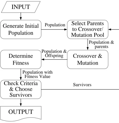
The genetic algorithm (GA) is a method which explores the design space to find a local optimal solution. The basic idea of GA comes from the Darwin's “The
Origin of Species”. Darwin's theory claimed that the evolution of species consists
of four steps: crossover, mutation, natural selection, and survival of the fitness. These four steps are also the main steps of genetic algorithm. Fig. 1 shows the simple flowchart of genetic algorithm. The first step of genetic algorithm is to generate initial population. Then, through crossover and mutation operations, new population is created from its parents. The crossover operation exchanges the individuals' genes to produce the offspring, and the mutation operation makes difference on individual's genes. The next step of GA is to choose favorable individuals. Finally, stopping criteria will be checked to determine whether or not the next loop will be executed. The detailed treatment can be found in [15].
Generally, the process of simulated annealing is hard to parallelize, but the genetic algorithm is a naturally parallel algorithm. However, the genetic algorithm is hard to converge to a good result. The proposed GASA (Genetic Algorithm based Simulated Annealing) algorithm inherits strengths from both GA and SA, and gets rid of the disadvantages of them. The GASA can be easily implemented in parallel. By parallelizing the algorithm, several machines can execute in parallel to speed up the computing time. Besides, the design space can be explored by performing neighborhood operation from SA.
Generate Initial
Population
Crossover &
Mutation
Check Criteria
& Choose
Survivors
Select Parents
to Crossover/
Mutation Pool
Determine
Fitness
Population
Population &
parents
Survivors
Population &
Offspring
Population with
Fitness Value
INPUT
OUTPUT
3. The proposed GASA scheduling algorithm
In this section, our GASA (Genetic Algorithm based Simulated Annealing) scheduling method is presented. First, we describe the problem of high level synthesis. Then, we introduce the data flow of the GASA algorithm. Third, we talk about the dual Vdd and dual Vth library. And fourth, the chromosome representation and some GASA operations and parameters are introduced in detail. Finally, the GASA algorithm and an example of the GASA scheduling are illustrated.
3. 1.
Problem Formulation
When given two supply voltages (Vdd_H, Vdd_L), two threshold voltages (Vth_H,
Vth_L), and a CDFG G =
〈
V, E〉
, which consist of k nodes (n1, n2, …, nk), we define the power consumption of the operation node na which operates with supply voltage Vdd_i and threshold voltage Vth_j, asP
Vdd_i,Vth_j(
n
a)
, and its delay time as)
(
_ _ ,V a Vn
D
j th idd . Now, we define the total power consumption of a given CDFG G as
}
,
{
and
,
}
,
{
where
,
)
(
_ _ _ _ _ _ , _ _ dd i dd H dd L th j th H th L G n a V Vn
V
V
V
V
V
V
P
TP
a j th i dd∈
∈
=
∑
∈ ∀and the total delay time as
}
,
{
and
,
}
,
{
where
,
)
(
_ _ _ _ _ _ of path critical , _ _ dd i dd H dd L th j th H th L G n b V Vn
V
V
V
V
V
V
D
TD
b j th i dd∈
∈
=
∑
∈ ∀Accordingly, we may further define the total power consumption of a given CDFG after ASAP (As Soon As Possible) scheduling as TPASAP and the delay as
be as large as possible, and the delay overhead should be as small as possible. Therefore, we define the gain of using GASA as
ASAP GASA GASA ASAP TD TD TP TP Gain − − =
where TPASAP
-
TPGASA is the power saving and TDGASA-
TDASAP is the delayoverhead compared with ASAP scheduling. The goal of this project is to maximize the Gain value.
3. 2.
Data flow of GASA
The GASA algorithm runs with several simulated annealing processes in parallel. The mutation operation in GA is analogical to the neighborhood operation in SA, and crossover operation represents the role of recombining independent solutions. Before we come to the GASA flow, one term must be defined first.
Definition: A Boltzmann trial is defined as a competition between states i and j, and the probability of state i wins the competition is 1/(1 (Ei Ej)/T)
e −
+ . Here, e is the natural constant, and Ei and Ej denote as the energy of state i and state j
respectively. T represents the temperature in the SA algorithm.
By the definition, the energy Ei and Ej represent the power-delay products of
the scheduling results. If the power-delay product of state i is smaller than that of
state j, then we define Ei < Ej. What should be noted is that if temperature T is large
enough, then the next state j will be accepted even the energy of j is larger than the
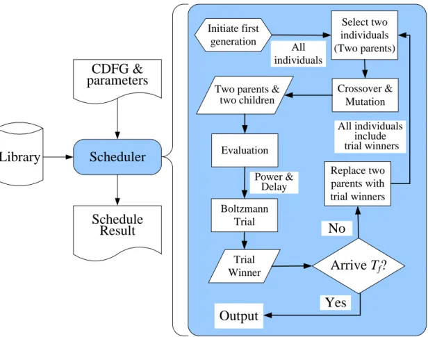
The data flow of the GASA algorithm is shown in Fig. 2. In this flow, the
inputs are the CDFG (Control/Data Flow Graph) and some parameters. The main
scheduler assigns different Vdd and Vth to each node in the CDFG. Thus, a library
which consists of several dual Vdd / Vth components is necessary to the scheduler.
At the beginning of the scheduler, it brings out the first generation, and generates
many individuals. Then, it randomly selects two individuals as the parents, and
performs the crossover and mutation operations to generate two children. After that,
the scheduler evaluates the power and delay of two parents and two children, and
decides the Boltzmann trial winner by Definition 1. If the temperature cools down
to the Tf (terminated temperature), it will output the trial winner, else it will
continue the GASA loop.
In our scheduling algorithm, we try to recombine the results of each individual
rather than just randomly generate a new individual. By combining the results of
each individual, we can improve the convergence speed. The recombining phase
will select two parents from the selection pool and produce two children. The two
children may have some essential parts of genes that make the fitness of the
children better or worse than that of their parents. Here, the “essential” parts of
genes represent those nodes belonging to the critical paths, or reducing large
Scheduler
CDFG &
parameters
Library
Schedule
Result
Replace two parents with trial winners Select two individuals (Two parents) Crossover & Mutation Evaluation Boltzmann TrialArrive T
f?
Initiate first generation Trial Winner All individuals Power & DelayYes
No
Output
Two parents & two children
All individuals include trial winners
Fig. 2. The GASA scheduling algorithm flowchart.
3. 3.
Dual V
dd/ V
thlibrary
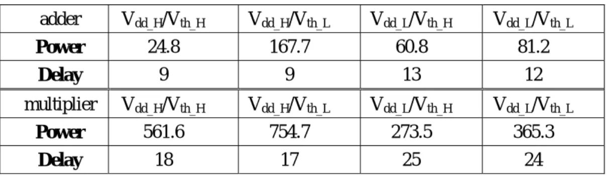
An essential component of the GASA algorithm is the cell library, in which
each cell has four instance types, as shown in Table 1. Table 1 shows the power and
delay of a 4-bit multiplier and a 4-bit adder with different Vdd and Vth. Here Vdd_H
represents a cell with high supply voltage. Similarly, Vth_L means a cell with low
threshold voltage. In order to simplify the calculation, the delay of each instance
Table 1. A technology library with dual Vdd and dual Vth adder Vdd_H/Vth_H Vdd_H/Vth_L Vdd_L/Vth_H Vdd_L/Vth_L Power 24.8 167.7 60.8 81.2 Delay 9 9 13 12 multiplier Vdd_H/Vth_H Vdd_H/Vth_L Vdd_L/Vth_H Vdd_L/Vth_L Power 561.6 754.7 273.5 365.3 Delay 18 17 25 24
Table 2. Chromosome representation One individual
n1 n2 … nk
Relative CS 0 1 … 1 Instance (Vdd/Vth) L/H H/L … L/L
3. 4.
Individual and Chromosome Representation
A suitable chromosome representation is needed to represent the individual in
the GASA scheduling algorithm, since it affects the running time of the algorithm.
The chromosome representation must include the information of supply voltage,
threshold voltage and control cycles. Table 2 shows the chromosome representation
in our GASA algorithm. In Table 2, ni denotes the ith node in the data flow graph,
the relative cs of ni shows the number of control steps between the starting control
step of ni and the maximum occupied control step of all preceding nodes of ni. The
instance records what kind of resources allocated to this operation; H indicates the
high voltage and L indicates the low voltage. By checking the instance field of one
node, we can look up the power consumption, area cost, and delay information
from the library. Each column in the table represents a chromosome. If there are k
3. 5.
GASA Operations and Parameters
1.5.1 Mutation operation
While performing the mutation operation on one individual, we will choose
some chromosomes to mutate their values by a specific mutation rate. For example,
if there are k nodes in one individual, and the mutation rate is Pm. We will choose k × Pm chromosomes to mutate, while randomly changing the genes (Relative CS
and instance). Through mutation operation, some variants of one individual can be
produced to explore the neighbors of the current position in design space. Later we
shall give a discussion on the mutation rate Pm.
1.5.2 Crossover operation
Crossover is a kind of recombination operation. Fig. 3 shows an example of
the crossover operation. In the GASA scheduling, we adopt one point crossover
operation which will exchange the right half part of two individuals to each other.
We also adopt uniform crossover operation which randomly exchanges some
chromosomes of two parents.
1.5.3 Population size
The population size is one of the major control parameters of the GASA.
1.5.4 Cooling procedure
The cooling procedure in our GASA scheduling is to multiply the current
temperature by a cooling constant CC (0<CC<1). If CC is set to a large value, the
temperature would reduce slowly and it would produce large generations. In
generally, the population size and the cooling constant both affect the optimization
gain and the computing time. The designer should tune both parameters to meet the
design constraints.
1.5.5 Mutation rate
The value of mutation rate will affect the difference between parents and
children. If the mutation rate is too large, some good chromosomes will be
annihilated. If the mutation rate is too small, the resemblance between parents and
children will be too close. Therefore, it will result in a local minimal solution. In
our algorithm, we set the mutation rate as 20%. A larger mutation rate is set if the
result seems to fall in a local minimal value.
1.5.6 Temperature
The last two parameters are the starting temperature Ts and terminating
temperature Tf. We set the terminating temperature as 0.1. The starting temperature
Ts is set by the mathematical method.
) 1 ln(1− − − = k i j s E E
T , where Ej and Ei is the initial
energy of state i and j, and k is the probability of Ei larger than Ej. The starting
temperature influences the convergence speed and the accepting rate of the parent
Parent A Parent B Child A Child B Node Relative CS Instance ( Vdd / Vth) L / L L / H H / H H / L N1 N2 N3 N4 N5 N6 0 1 1 3 0 1 H / H H / L Node Relative CS Instance ( Vdd / Vth) H / L H / H L / H L / L N1 N2 N3 N4 N5 N6 1 2 0 3 1 1 L / L L / H Node Relative CS Instance ( Vdd / Vth) H / L H / H N1 N2 N3 N4 N5 N6 1 2 0 3 0 1 L / H Node Relative CS Instance ( Vdd / Vth) L / H L / L N1 N2 N3 N4 N5 N6 3 1 1 L / L H / H H / H H / L L / L L / H 0 1 1 H / L
Fig. 3. An example of one point crossover operation.
3. 6.
GASA Algorithm
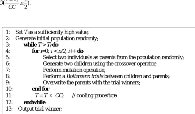
Fig. 4 shows the GA-based simulated annealing algorithm. In this algorithm,
the convergence rate is controlled by temperature T and the cooling constant CC. In
line 1, the initial temperature T is set to a sufficiently high value, so that uphill
probability will be greater than 50%. From the code segment of line 3 to line 12 in
Fig. 4, the while loop performs the temperature control of SA. The inner loop (from
line 4 to line 10) represents the neighborhood operation of SA. Through the
neighborhood operation, the solution space can be explored. In line 7, the Boltzmann trial is used to decide whether the uphill operation should be accepted
)
(
n) (
CC T T
O − f . Thus, the total time complexity of the GASA algorithm is ) 2 ( n CC T T O − f × .
Fig. 4. Genetic algorithm based simulated annealing algorithm.
3. 7. Example of GASA Scheduling
Suppose we have a library which consists of several components. Each
component was implemented with four different kinds of the Vdd / Vth
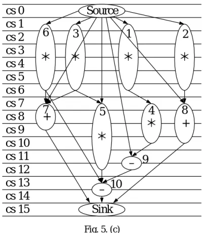
combination, as shown in Table 1. The input file is the DFG, as shown in Fig. 5.(a).
At the beginning, each node is assigned with different Vdd and Vth. After several
loops, the scheduling result was shown in Fig. 5.(c), and the Vdd / Vth assignment
was shown in Fig. 5.(b). Note that the different instances used in the scheduling
process influence the final delay and the power consumption of whole design. 1: Set T as a sufficiently high value;
2: Generate initial population randomly; 3: while T > Tf do
4: for i=0; i < n/2; i++ do
5: Select two individuals as parents from the population randomly; 6: Generate two children using the crossover operator;
7: Perform mutation operation;
8: Perform a Boltzmann trials between children and parents; 9: Overwrite the parents with the trial winners;
10: end for
11: T = T × CC; // cooling procedure 12: endwhile
The goal of GASA is to maximize the Gain value of a system according to the
cost function. Through our genetic algorithm based simulated annealing approach,
the nearly optimal solution can be achieved in a tolerable processing time.
Sink Source
*
*
*
*
+
*
*
+
–
–
Fig. 5 (a) Node 1 2 3 4 5 6 7 8 9 10 Instance (Vdd/Vth) L/H L/H L/H L/H L/H L/H L/L L/H H/H H/H Fig. 5 (b)cs 0
cs 1
cs 2
cs 3
cs 4
cs 5
cs 6
cs 7
cs 8
cs 9
cs 10
cs 11
cs 14
cs 15
cs 12
cs 13
Source
Sink
*
*
*
*
+
*
+
*
–
–
1
2
3
4
5
6
7
8
9
10
Fig. 5. (c)Fig. 5. An example of GASA scheduling. (a) Original DFG. (b) Vdd/Vth of
each node. (c) Scheduling result.
4. Experimental Result
To show the effectiveness of our method, we compare the power consumption
and delay overhead among three scheduling algorithms. The first is the ASAP (As
Soon As Possible) scheduling method. The second is the dual Vdd only scheduling
method, and the third is the proposed dual Vdd and dual Vth scheduling method. A
dual Vdd/Vth library, as shown in Table 1, which contains three components
(multiplier, adder, and multiplexer), is used for low power scheduling. In this
library, each component was designed by TSMC 0.18μm process. The Vdd_H was
The experimental result is shown in Table 3. Six CDFG benchmarks are used
to examine the scheduling algorithms. It is clearly that the proposed dual Vdd/Vth
can obtain the best power-delay product, and it also shows the proposed method
can obtain about 46.1% power saving and 12.3% delay overhead compared with
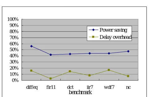
the ASAP scheduling method. Fig. 6 shows the comparison of power saving and
delay overhead between ASAP scheduling and dual Vdd/Vth scheduling methods.
In this figure, the solid lines represent the dual Vdd/Vth scheduling relative to the
ASAP method.
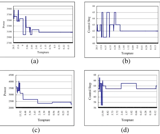
We also show the convergence result of diffeq benchmark. Fig. 7.(a) and (b)
are the power and delay convergence result by using dual Vdd only scheduling
method. Fig. 7.(c) and (d) indicate the power and delay convergence result by using
dual Vdd and dual Vth scheduling method.
The experimental result shows that we can get further power reduction when
using a dual Vdd and dual Vth library with limited delay overhead. It means that
the proposed method has a tradeoff between power consumption and delay. In this
algorithm, most controlling parameters can be set automatically to reduce the
designers' loading. More constraints can be added to this algorithm such as area
constraints, and the additional penalty so that it can provide more flexible design
Table 3. Experimental result.
ASAP scheduling Dual Vdd scheduling Dual Vdd/Vth scheduling Bench-
mark Power Delay Power×
Delay Power Delay
Power×
Delay Power Delay
Power× Delay diffeq 5199.4 54 280767.6 3079.0 62 190898 2300.2 64 147212.8 fir11 9979.5 109 1087765.5 435.7 130 706641 5797.9 112 649364.8 dct 16436.8 72 1183449.6 10941.0 83 908103 9332 84 78388 iir7 13669.3 144 1968379.2 8519.8 158 1346128.4 7656.9 156 1194476.4 wdf7 17023.8 125 2127975 10576.0 150 1586400 948.1 150 1422765 nc 28177.3 135 3803935.5 17834.9 151 2693069.9 14814.2 145 2148059 0% 10% 20% 30% 40% 50% 60% 70% 80% 90% 100%
diffeq fir11 dct iir7 wdf7 nc
benchmark
Power saving Delay overhead
Fig. 6. A comparison of power saving and delay overhead between ASAP
2700 2900 3100 3300 3500 3700 3900 20. 5 13. 6 9 5. 96 3. 95 2. 6 1 1. 73 1. 15 0. 76 0.5 0. 33 0. 22 0. 15 Tempture Po w e r 60 61 62 63 64 65 66 20 .5 13. 9 9. 37 6. 33 4. 28 2. 89 1. 9 5 1. 32 0. 89 0.6 0. 41 0. 28 0. 19 0. 13 Tempture Co n tro l S te p 2000 2500 3000 3500 4000 4500 13. 32 8. 48 5. 39 3. 43 2. 18 1. 39 0. 88 0. 56 0. 36 0. 23 0. 14 Tempture Po w e r 56 58 60 62 64 66 68 13. 5 9 8. 82 5. 73 3. 72 2. 41 1. 57 1. 02 0. 66 0. 43 0. 28 0. 18 0. 12 Tempture Co n tr o l S te p
(a)
(b)
(c)
(d)
Fig. 7 Convergence result of diffeq benchmark. (a) power result with dual Vdd.
(b) delay result with dual Vdd. (c) power result with dual Vdd/Vth. (d) delay
5. Conclusion
In this project, a dual Vdd / Vth scheduling method is proposed for low power
high level synthesis. In the proposed method, the dynamic and static power
consumption are considered simultaneously. By using the GASA (genetic
algorithm based simulated annealing) algorithm, each node in the CDFG (Control
Data Flow Graph) is assigned with either a high or low Vdd / Vth to achieve the
low power goal and to control the computing time. The experimental result shows
that our method is feasible. The contribution of this project is that the GASA
method can be used on multiple Vdd / Vth scheduling and takes both power and
參考文獻
[1] http://public.itrs.net/
[2] M. A. Elgamel, and M. A. Bayoumi, “On low power high level synthesis using genetic algorithm,” in IEEE Proc. of ICECS 2002, Vol 2. pp. 725-728, Sept. 2002.
[3] S. P. Mohanty, and N. Ranganathan, “A framework for energy and transient power reduction during behavioral synthesis,” IEEE Trans. on VLSI system, Vol. 12 No. 6, pp 562-572, June 2004.
[4] L. R. Dung, and H. C. Yang, “On multiple-voltage high-level synthesis using algorithmic transformations,” IEICE Trans. Fundamentals, Vol. E87-A, No. 12, pp 3100-310, Dec. 2004.
[5] J. M. Chang, and M. Pedram, “Energy minimization using multiple supply voltages,” IEEE Trans. on VLSI system, Vol. 5, No. 4, pp. 436-443, Dec. 1997. [6] J. Y. Choi, C. H. Lin, and H. S. Kim, “A low power register scheduling and
allocation algorithm for multiple voltage,” in Proc. IEEE TENCON, Vol. 2, pp. 627-630, Aug. 2001.
[7] A. Nanzak, and C. Chakrabarti, “A low power scheduling scheme with resources operating at multiple voltage,” Trans. on IEEE VLSI systems, Vol. 2, issues 1. pp. 6-14, Feb. 2002.
[8] K. Usami, and M. Igarashi, “Low-power design methodology and application utilizing dual supply voltage,” in IEEE Proc. of ASP-DAC, pp. 123-128, Jan. 2000.
[9] C. Piguet, Low-Power Electronics Design, CRC Press, 2004.
[10] D. Samanta, and A. Pal, “Synthesis of dual-V/sub T/ dynamic CMOS circuits,” in Proc. of VLSI Design 2003, pp. 303-308, Jan. 2003.
[11] K. S. Khouri, and N. K. Jha, “Leakage Power Analysis and Reduction During Behavioral Synthesis,” IEEE Trans. on VLSI systems, Vol. 10, No. 6, pp. 876-885, Dec. 2002.
[12] S. Augsburger, and B. Nikolic, “Combing dual-supply, dual threshold and transistor sizing for power reduction,” in IEEE Proc. of ICCD’02, pp. 31-321, Sept, 2002.
applications, Kluwer Academic Publishers, 1987.
[15] P. Mazumder, E. M. Rudnick, Genetic algorithm for VLSI design, layout & test automation, Prentie Hall PTR, 1999.
計畫成果自評
I. 原訂計畫目標:
第二年計畫的研究核心在於設計出一種新的低功率電路設計方法,並利 用這種方法來解決大型電路設計上的功率消耗問題。利用此方法將可滿足部 分奈米製程之設計。此外,我們將藉由資訊理論與人工智慧演算法,配合第 一年計畫所提出之低功率元件模組,建立一個有效的設計資料庫。II. 研究內容與原計畫相符程度
完全符合。III. 預期目標達成情況與綜合自評
在本年度的計畫中,我們提出了一個在高層次(high-level)設計低功率電路的新方法。此方法結合基因演算法(Genetic Algorithm)與模擬退火法(Simulated Annealing)將高層次的資料控制流程圖(CDFG)中的元件重新予以排程。元件的 選擇係利用雙重供應電壓(Dual supply voltage)與雙重臨界電壓(Dual threshold voltage)來達到節省功率消耗的目的。於高層次進行低功率方法設計的主要優 點在於處理大型電路時,較能掌控整體系統,並且獲得較多的消耗功率改善。 面對大型系統,往較高層次方向設計電路儼然將成為未來之趨勢。此外,在 實驗環境中,我們雖利用台灣積體電路股份有限公司的 0.18μm 製程來進行 模擬,但若將排程時的元件資料庫更新為奈米製程之元件,本方法亦可被利 用,且將更能得到顯著之成果,因此,本方法與預期目標中之滿足部分奈米 製程設計完全相符。本項計畫在台大資工系賴飛羆教授的帶領與督導下,研 究進行的進度與原先計畫的進度完全一致,而研究成果更發表於國際知名的
IV. 學術成果發表
(1) Kun-Lin Tsai, Szu-Wei Chang, Feipei Lai, and Shanq-Jang Ruan, “A Low Power Scheduling Method using Dual Vdd and Dual Vth,” in Proc. of IEEE
International Symposium on Circuits and Systems, May 2005. (第二年計畫研 究成果)
(2) Kun-Lin Tsai, Shanq-Jang Ruan, Li-Wei Chen, Feipei Lai, and Edwin Naroska, “Low Power Dynamic Bus Encoding for Deep Sub-micron Design,” in Proc. of
The 3rd International IEEE Northeast Workshop on Circuit & System, June
2005. (第一年研究計畫成果)
(3) Kun-Lin Tsai, Szu-Wei Chang, Shanq-Jang Ruan, and Hsiu-Hui Lee, “Low Power Scheduling with Dual Supply Voltages and Dual Threshold Voltages,” submitted to IEICE Trans. on Fundamentals of Electronics, Communications