Abstract—The RC-based power-rail electrostatic-discharge
(ESD) clamp circuit with big field-effect transistor (BigFET) layout style in the main ESD clamp n-channel metal–oxide– semiconductor (NMOS) transistor was widely used to enhance the ESD robustness of a CMOS IC fabricated in advanced CMOS processes. To further reduce the occupied layout area of the RC in the power-rail ESD clamp circuit, a new ESD-transient detection circuit realized with smaller capacitance has been proposed and verified in a 0.13-μm CMOS process. From the experimental results, the power-rail ESD clamp circuit with the new proposed ESD-transient detection circuit can achieve a long-enough turn-on duration and higher ESD robustness under ESD stress condition, as well as better immunity against mistrigger and latch-on event under the fast-power-on condition.
Index Terms—Electrostatic discharge, ESD protection design,
ESD-transient detection circuit, power-rail ESD clamp circuit. I. INTRODUCTION
W
ITH the era of advanced nanoscale CMOS technology, electrostatic discharge (ESD) protection has become a tough task on the product reliability of CMOS integrated circuits. The scaled-down device dimension with thinner gate oxide and shallower junction depth in nanoscale CMOS tech-nology is easily damaged by ESD stress. The power-rail ESD clamp circuit is an efficient design to achieve whole-chip ESD protection in IC products [1], [2]. It can not only enhance the ESD robustness of VDD-to-VSS ESD stress but can also significantly improve the ESD robustness of the ESD stresses between the input/output and VDD/VSS [2]. To efficiently protect the core circuits realized with much thinner gate oxide in nanoscale CMOS technology, some studies had reported the efficient n-channel metal–oxide–semiconductor (NMOS)-based power-rail ESD clamp circuits without snapback opera-tion [3]–[11]. In such a power-rail ESD clamp circuit, the main ESD clamp NMOS transistor can thoroughly discharge a hugeManuscript received October 15, 2008; revised February 2, 2009. Current version published May 15, 2009. This work was supported by the SoC Tech-nology Center, Industrial TechTech-nology Research Institute, Hsinchu, Taiwan. This paper was recommended by Associate Editor K.-P. Pun.
S.-H. Chen is with the Nanoelectronics and Gigascale Systems Labora-tory, Institute of Electronics, National Chiao-Tung University, Hsinchu 30050, Taiwan, and also with the SoC Technology Center, Industrial Technology Research Institute, Hsinchu 310, Taiwan (e-mail: shchen@itri.org.tw).
M.-D. Ker is with the Institute of Electronics, National Chiao-Tung Univer-sity, Hsinchu 30050, Taiwan, and also with the Department of Electronic Engi-neering, I-Shou University, Kaohsiung 840, Taiwan (e-mail: mdker@ieee.org). Color versions of one or more of the figures in this paper are available online at http://ieeexplore.ieee.org.
Digital Object Identifier 10.1109/TCSII.2009.2019164
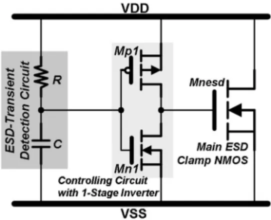
Fig. 1. Typical implementation of the RC-based power-rail ESD clamp circuit with ESD-transient detection circuit, controlling circuit, and main ESD clamp NMOS.
ESD current by its channel current to exhibit excellent turn-on efficiency with lower trigger voltage (Vt1) and lower clamped voltage (Vclamp). Most of them adopted the gate-driven mechanism [1]–[11], which was basically implemented by an
RC-based ESD-transient detection circuit and a controlling
circuit, to respectively command the main ESD clamp NMOS transistor into theONorOFFstate under ESD stress conditions and normal circuit operation conditions, as shown in Fig. 1. Two major different circuit schemes, i.e., the RC-time delay technique [1]–[9] and the capacitance-coupling mechanism [10], [11], were usually used as the ESD-transient detection cir-cuit in the power-rail ESD clamp circir-cuit. Then, the controlling circuit was implemented by single- or multi-stage inverters.
The main ESD clamp NMOS transistor without snapback operation has to be kept at the ON state for the whole
du-ration of the ESD events in order to ensure that the ESD current can be discharged by its channel current. Based on the traditional RC-based ESD-transient detection circuit [1], [2], the RC-time constant essentially dominated the turn-on dura-tion of the main ESD clamp NMOS transistor. Therefore, the
RC-time constant should be designed large enough to keep the
main ESD clamp NMOS with a long-enough turn-on duration in the power-rail ESD clamp circuit under ESD stress condition. In general, the turn-on duration was adjusted to meet the period of the human-body-model (HBM) ESD event, which is about several hundreds ns [12]. The extended RC-time constant not only accompanies the larger layout sizes of the resistance and capacitance but is also subject to mistrigger the main ESD clamp NMOS transistor under fast-power-on applications [7].
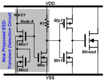
Fig. 2. Power-rail ESD clamp circuit with the new proposed ESD-transient detection circuit. The new proposed ESD-transient detection circuit is com-posed of a smaller capacitor (C1), cascode NMOS transistors (Mnc1 and Mnc2), a resistor (R1), and a switch NMOS transistor (Mns).
Several previous works proposed special circuit schemes with feedback circuit techniques to extend the turn-on duration under a small RC-time constant [5]–[7], [10], [11]. However, those feedback circuit designs always suffered from latch-on threats under the fast-power-on events or the electrical fast transient noise [13], [14]. In addition, other circuit schemes without feedback circuit techniques, such as on-time control circuits [6] and multi-RC-triggered circuits [8], had also been presented to achieve the desired turn-on duration and avoid the latch-on threat. However, extra resistances and capacitances have to be implanted into these designs, occupying quite more silicon area. In this work, a new ESD-transient detection circuit has been proposed and verified in 0.13-μm 1.2-V CMOS technology. This design abandons the feedback circuit techniques and adopts the capacitance-coupling mechanism to accomplish the desired function in commanding the main ESD clamp NMOS transistor. From experimental measurements, including turn-on efficiency, transmission line pulse (TLP) stress, ESD stress, and fast-power-on transition, the power-rail ESD clamp circuit with the new proposed ESD-transient detection circuit has presented a much better performance than the traditional design.
II. REALIZATION OFPOWER-RAILESD CLAMPCIRCUIT
A. Power-Rail ESD Clamp Circuit With the New Proposed ESD-Transient Detection Circuit
An area-efficient ESD-transient detection circuit with smaller capacitor that adopts the capacitance-coupling mech-anism to achieve the required functions on the power-rail ESD clamp circuit has been shown in Fig. 2. This area-efficient ESD-transient detection circuit consists of a smaller capacitor (C1), cascode NMOS transistors (Mnc1 and Mnc2), a resistor (R1), and a switch NMOS transistor (Mns) that commands the main ESD clamp NMOS transistor through a controlling circuit with a single-stage inverter. The smaller capacitor is implemented by metal–oxide–metal parasitic capacitance. The cascode NMOS transistors are used as a large resistor and combined with the smaller capacitor to construct a capacitance-coupling network
Fig. 3. Comparison on the layout areas between the power-rail ESD clamp circuits with (a) the traditional and (b) new proposed ESD-transient detection circuits.
[15], [16]. Node A between the smaller capacitor and the cascode NMOS transistors is connected to the gate terminal of the switch NMOS transistor. Then, its drain terminal is tied to the VDD through the resistor and also connected to the input of the controlling circuit. Such a circuit technique, which is similar to capacitive boosting via current amplification, was also used in some voltage regulation circuits [17], [18].
Through the controlling circuit, the switch NMOS transistor can rule the main ESD clamp NMOS transistor to remain at the ON or OFF state. Finally, the main ESD clamp NMOS transistor has been drawn with the BigFET layout style, which has a minimum drain-contact-to-polygate spacing of 0.25 μm, and without silicide blocking on its diffusion in a 0.13-μm 1.2-V CMOS process. Compared with the layout area of the power-rail ESD clamp circuit with the traditional RC-based ESD-transient detection circuit, this work with the new pro-posed ESD-transient detection circuit is smaller, as shown in Fig. 3(a) and (b). The cell height of the whole power-rail ESD clamp circuit is reduced by about 13%, and the layout area of the ESD-transient detection circuit is reduced about 50%, by using the new proposed ESD-transient detection circuit.
B. Operation Principles
During the positive VDD-to-VSS ESD stress condition, the potential of node A will be synchronously evaluated toward a positive voltage potential by capacitance coupling of the smaller capacitor to trigger on the switch NMOS transistor. Then, through the switch NMOS transistor and the controlling circuit, the gate terminal of the main ESD clamp NMOS transistor will be promptly charged toward the positive voltage potential. The main ESD clamp NMOS transistor is turned on to clamp and discharge the huge ESD voltage and ESD current. The turn-on duration of the main ESD clamp NMOS transistor is dominated by the potential of node A. This potential is
Fig. 4. Simulation result of the voltage potential on the gate terminal of the main ESD clamp NMOS transistor in the power-rail ESD clamp circuit.
TABLE I
DESIGNPARAMETERS IN THEPOWER-RAILESD CLAMPCIRCUITWITH THENEWPROPOSEDESD-TRANSIENTDETECTIONCIRCUIT
synchronously kept at the positive voltage potential by the ca-pacitance coupling; however, it will be slowly pulled down due to the turned-on cascode NMOS transistors. Because the gate terminals of these two cascode NMOS transistors with small device dimensions have been connected to their drain terminals, they are operated at the saturation region to provide a larger resistance under the positive VDD-to-VSS ESD event. Finally, when the potential of node A is lower than the threshold voltage of the NMOS transistor, the switch NMOS transistor will be turned off to force the main ESD clamp NMOS transistor off. Based on the simulation result, the turn-on duration of the main ESD clamp NMOS transistor can achieve more than 600 ns in the power-rail ESD clamp circuit with a smaller capacitor of only∼10 fF, as shown in Fig. 4. The 3-V voltage pulse with a rise time of 2 ns was applied to the VDD node, with the VSS node grounded. The voltage potential on the gate terminal of the main ESD clamp NMOS transistor is higher than the threshold voltage of ∼0.35 V during the period of ∼620 ns. Although the turn-on duration can further be extended by directly enlarging the resistance, capacitance, and device sizes of the cascode NMOS and switch NMOS transistors, the unde-sired side effect, such as the degradation of immunity against mistrigger under fast-power-on condition, would also be in-duced. The detailed design parameters, such as the device sizes of the cascode NMOS transistors and switch NMOS transistor, have been listed in Table I. On the other hand, the parasitic drain-bulk diode of the main ESD clamp NMOS transistor can provide a low-impedance path under negative VDD-to-VSS ESD stress.
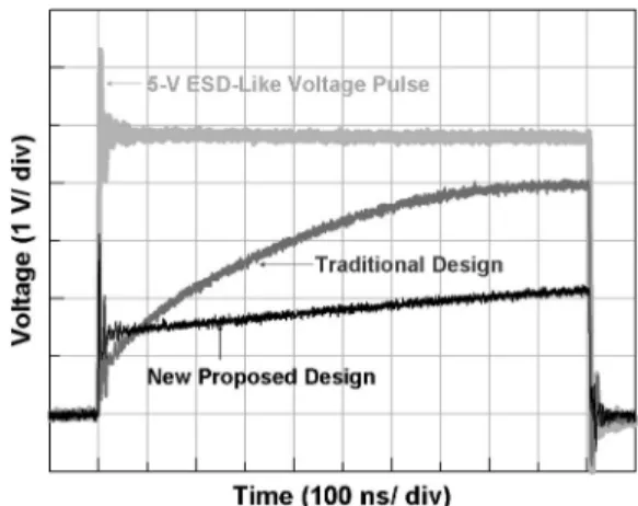
Fig. 5. Measured voltage waveforms of the power-rail ESD clamp circuits with the traditional and new proposed ESD-transient detection circuits under 5-V ESD-like voltage pulses with 2-ns rise time.
Under the normal power-on condition, the normal VDD power-on voltage waveform has a rise time on the order of mil-liseconds. Such a power-on voltage waveform will not produce enough coupling potential on node A to trigger on the switch NMOS transistor. The potential of node A will actually be kept at ground through the high resistance path of the cascode NMOS transistors. Therefore, the main ESD clamp NMOS transistor will be kept at theOFFstate under the normal circuit operation condition. In addition, the power-rail ESD clamp circuit with the new proposed ESD-transient detection circuit also presents high immunity against mistrigger and latch-on events.
III. EXPERIMENTALRESULT
A. Turn-On Verification Under ESD-Like Stress Condition
In order to observe the turn-on efficiency of the power-rail ESD clamp circuit with the new proposed ESD-transient detection circuit, 2.4-V and 5-V ESD-like voltage pulses with 2-ns rise time are applied to the VDD terminal, with the VSS terminal grounded. The voltage pulses with a rise time of 2 ns and a duration of 1 μs generated from a pulse generator are used to simulate the fast-rising edge of the HBM ESD event [12]. The sharp-rising edge of the ESD-like voltage pulse will be detected by the ESD-transient detection circuit and then used to turn on the switch NMOS transistor. The main ESD clamp NMOS transistor is therefore triggered on by the controlling circuit. When the main ESD clamp NMOS transistor is turned on, the voltage waveform on the VDD terminal will be clamped as the measured results shown in Fig. 5.
According to the measured results in Fig. 5, the new pro-posed design exhibits an excellent turn-on efficiency to clamp the overshooting voltage to a much lower voltage level. The voltage waveform of the new proposed design can constantly be clamped by the turned-on main ESD clamp NMOS transistor during the whole 1-μs pulsewidth. On the contrary, the voltage waveform of the traditional design will quickly rise, and its clamped voltage will be much higher than that of the new proposed design after the duration of 200 ns. The new pro-posed ESD-transient detection circuit can efficiently extend the turn-on duration of the main ESD clamp NMOS transistor in
Fig. 6. TLP I–V curves of the power-rail ESD clamp circuits with the traditional and new proposed ESD-transient detection circuits.
TABLE II
HBMANDMM ESD ROBUSTNESS OF THEPOWER-RAILESD CLAMP
CIRCUITSWITH THETRADITIONAL ANDNEWPROPOSED
ESD-TRANSIENTDETECTIONCIRCUITS
the power-rail ESD clamp circuit. The longer turn-on duration of the main ESD clamp NMOS transistor would assure that the low-impedance path was entirely provided from VDD to VSS under the whole HBM ESD event and would also enhance the ESD robustness of the power-rail ESD clamp circuit.
B. TLPI–V Characteristics and ESD Robustness
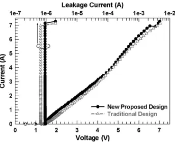
The TLP-measured [19] I–V characteristics of the power-rail ESD clamp circuits with the traditional and new proposed ESD-transient detection circuits are shown in Fig. 6. This TLP system has a 100-ns pulsewidth and a 2-ns rise time. These two power-rail ESD clamp circuits present the desired TLP I–V characteristics, where the main ESD clamp NMOS transistors in these two designs are the same in device dimensions and layout style. No obvious difference among the TLP measured results was observed between these two designs. The second breakdown currents (It2) of these two power-rail ESD clamp circuits can achieve more than 7 A. Their clamped voltages (Vclamp) and on resistances (Ron) are similar.
Table II shows the HBM [12] and machine-model (MM) [20] ESD robustness of these two power-rail ESD clamp circuits. The HBM and MM ESD robustness of the power-rail ESD clamp circuit with the new proposed ESD-transient detection circuit are 8.0 kV and 400 V, respectively, which are obviously higher than those of the power-rail ESD clamp circuit with the traditional ESD-transient detection circuit. According to failure analysis using scanning-electron-microscopy observa-tion, the failure spot of the traditional design is located on the unexpected junction melting damages between the n+/n-well minority guard ring and the p+ majority guard ring after 6.0-kV HBM ESD stress, as shown in Fig. 7(a) and (b). Because
Fig. 7. (a) Failure spot of the power-rail ESD clamp circuit with the traditional ESD-transient detection circuit after 6.0-kV HBM ESD stresses. (b) Zoomed-in view of the failure spot at location A.
the power-rail ESD clamp circuit with the traditional ESD-transient detection circuit has insufficient turn-on duration, the huge ESD current could not efficiently discharge during the whole HBM ESD event to induce the unexpected failure spot after 6.0-kV HBM ESD stress.
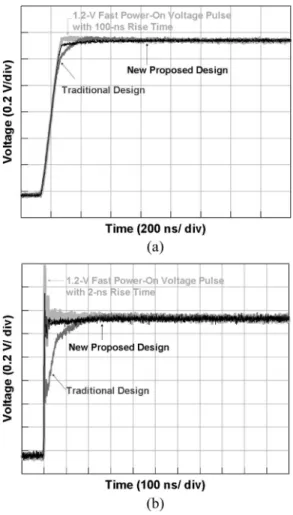
C. Fast-Power-On Condition and Discussion
In general, the normal VDD power-on voltage waveform has a rise time on the order of milliseconds and an amplitude of VDD operation voltage. Due to such a slow rise time and a small amplitude in normal power-on conditions, the coupling potential on node A is too weak to turn on the switch NMOS transistor. Therefore, the main ESD clamp NMOS transistor will be well kept at the OFF state. In this work, both
power-rail ESD clamp circuits with the traditional and new proposed ESD-transient detection circuits can successfully achieve the desired task under normal power-on conditions. However, some previous studies [6]–[8], [13], [14] have illustrated that several power-rail ESD clamp circuits with RC-based ESD-transient detection circuits and feedback circuit schemes were easily mis-triggered and were in the latch-on state under the fast-power-on conditions, with the rise time on the order of nanoseconds. The design with the new proposed ESD-transient detection circuit has been applied with 1.2-V voltage pulses with 100- or 2-ns rise time, both of which are used to simulate the fast-power-on condition, to investigate its immunities against mistrigger and latch-on events. The measured results are shown in Fig. 8(a) and (b), respectively. Its measured voltage waveforms do not show any obvious degradation under the fast-power-on con-dition with a voltage pulse of 1.2 V and a rise time of 100 or 2 ns. On the contrary, the power-rail ESD clamp circuit with the traditional ESD-transient detection circuit suffered from the mistrigger under the fast-power-on conditions. Its voltage waveforms will be slightly degraded under the 1.2-V fast-power-on pulse with 100-ns rise time and dramatically degraded under that with 2-ns rise time.
Since the feedback circuit schemes were not used in this work, the latch-on event was not observed in these two power-rail ESD clamp circuits. Compared with the results in the previous studies [6]–[8], [10], [11], the power-rail ESD clamp circuit with the new proposed ESD-transient detection circuit possesses excellent immunity against mistrigger and latch-on event. Because the new proposed ESD-transient detection cir-cuit adopts the capacitance-coupling mechanism, this new pro-posed design not only distinguishes the abnormal overshooting
Fig. 8. Measured voltage waveforms of the power-rail ESD clamp circuits with the traditional and new proposed ESD-transient detection circuits under the 1.2-V fast-power-on condition with (a) 100- and (b) 2-ns rise times.
voltage pulse by its rise time but also discriminates this volt-age pulse by its voltvolt-age amplitude. The new proposed ESD-transient detection circuit can easily distinguish the ESD event from the fast-power-on condition with the voltage amplitude of 1.2 V and the rise time of 2 ns.
IV. CONCLUSION
A new ESD-transient detection circuit with a smaller ca-pacitance of only 10 fF for use in the on-chip power-rail ESD protection design has been proposed and successfully verified in 0.13-μm CMOS technology. The new proposed ESD-transient detection circuit adopts the capacitance-coupling mechanism and a switch NMOS transistor to command the main ESD clamp NMOS transistor through the controlling circuit of a single-stage inverter. According to the measured results, the power-rail ESD clamp circuit with the new proposed ESD-transient detection circuit exhibits superior ESD robust-ness of 8.0 kV and 400 V in HBM and MM ESD stresses,
Electron Devices, vol. 46, no. 1, pp. 173–183, Jan. 1999.
[3] E. Worley, R. Gupta, B. Jones, R. Kjar, C. Nguyen, and M. Tennyson, “Sub-micron chip ESD protection schemes which avoid avalanching junction,” in Proc. EOS/ESD Symp., 1995, pp. 13–20.
[4] T. Maloney and W. Kam, “Stacked PMOS clamps for high voltage power supply protection,” in Proc. EOS/ESD Symp., 1999, pp. 70–77. [5] S. Poon and T. Maloney, “New considerations for MOSFET power
clamps,” in Proc. EOS/ESD Symp., 2002, pp. 1–5.
[6] M. Stockinger, J. Miller, M. Khazhinsky, C. Torres, J. Weldon, B. Preble, M. Bayer, M. Akers, and V. Kamat, “Boosted and distributed rail clamp networks for ESD protection in advanced CMOS technologies,” in Proc.
EOS/ESD Symp., 2003, pp. 17–26.
[7] J.-J. Li, R. Gauthier, and E. Rosenbaum, “A compact, timed-shutoff, MOSFET-based power clamp for on-chip ESD protection,” in Proc.
EOS/ESD Symp., 2004, pp. 273–279.
[8] J.-J. Li, R. Gauthier, S. Mitra, C. Putnam, K. Chatty, R. Halbach, and C. Sequin, “Design and characterization of a multi-RC-triggered MOSFET-based power clamp for on-chip ESD protection,” in Proc.
EOS/ESD Symp., 2006, pp. 179–185.
[9] O. Quittard, Z. Mrcarica, F. Blanc, G. Notermans, T. Smedes, and H. Zwol, “ESD protection for high-voltage CMOS technologies,” in Proc.
EOS/ESD Symp., 2006, pp. 77–86.
[10] J. Smith and G. Boselli, “A MOSFET power supply clamp with feedback enhanced triggering for ESD protection in advanced CMOS technolo-gies,” in Proc. EOS/ESD Symp., 2003, pp. 8–16.
[11] J. Smith, R. Cline, and G. Boselli, “A low leakage low cost-PMOS based power supply clamp with active feedback for ESD protection in 65 nm CMOS technologies,” in Proc. EOS/ESD Symp., 2005, pp. 298–306. [12] For Electrostatic Discharge Sensitivity Testing—Human Body Model
(HBM)—Component Level, ESD Association Standard Test Method ESD
STM5.1-2001, 2001.
[13] C.-C. Yen and M.-D. Ker, “Failure of on-chip power-rail ESD clamp circuits during system-level ESD test,” in Proc. IEEE Int. Rel. Phys.
Symp., 2007, pp. 598–599.
[14] M.-D. Ker and C.-C. Yen, “Unexpected failure in power-rail ESD clamp circuits of CMOS integrated circuits in microelectronics systems during electrical fast transient (EFT) test and the re-design solution,” in Proc.
IEEE Int. Zurich Symp. Electromagn. Compat., 2007, pp. 69–72.
[15] M.-D. Ker, C.-Y. Wu, T. Cheng, and H.-H. Chang, “Capacitor-couple ESD protection circuit for deep-submicron low-voltage CMOS ASIC,” IEEE
Trans. Very Large Scale Integr. (VLSI) Syst., vol. 4, no. 3, pp. 307–321,
Sep. 1996.
[16] J. Chen, A. Amerasekera, and C. Duvvury, “Desing methodology and optimization of gate-driven NMOS ESD protection circuits in submicron CMOS process,” IEEE Trans. Electron Devices, vol. 45, no. 12, pp. 2448– 2456, Dec. 1998.
[17] G. Giustolisi, G. Palumbo, and E. Spitale, “Low-voltage LDO compensa-tion strategy based on current amplifier,” in Proc. IEEE Int. Symp. Circuits
Syst., 2008, pp. 2681–2684.
[18] R. Milliken, J. Silva-Martinez, and E. Sanchez-Sinencio, “Full on-chip CMOS low-dropout voltage regulator,” IEEE Trans. Circuits Syst. I, Reg.
Papers, vol. 54, no. 9, pp. 1879–1890, Sep. 2007.
[19] T. Maloney and N. Khurana, “Transmission line pulsing techniques for circuit modeling of ESD phenomena,” in Proc. EOS/ESD Symp., 1985, pp. 49–54.
[20] For Electrostatic Discharge Sensitivity Testing—Machine Model (MM)—
Component Level, ESD Association Standard Test Method ESD