This content has been downloaded from IOPscience. Please scroll down to see the full text.
Download details:
IP Address: 140.113.38.11
This content was downloaded on 28/04/2014 at 20:15
Please note that terms and conditions apply.
A consistent model for carrier transport in heavily doped semiconductor devices
View the table of contents for this issue, or go to the journal homepage for more 1988 Semicond. Sci. Technol. 3 766
(http://iopscience.iop.org/0268-1242/3/8/006)
Semicond. Sci. Technol. 3 (1988) 766-772. Printed in the UK
K M Chang
Department of Electronics Engineering and Institute of Electronics, National Chiao Tung University, Taiwan, Republic of China
Received 7 January 1988, in final form 10 March 1988
Abstract. A self-consistent model for describing carrier transport in heavily doped semiconductor devices has been developed. The proposed model allows convenient treatment of non-uniform semiconductors i n a manner that is both thermodynamically consistent and consistent with the transport equations, the steady-state continuity equations and the electrostatic potetial with explicit boundary conditions at the contacts. The complex problems are reduced to determining two types of quantities: the reference electrostatic potential and the activity coefficient of the carriers. In order to find the simple working equations for the model, two choices of reference for the electrostatic potential are discussed. The presented transport equations are written in a simple Shockley-like form, in which the effects associated with the non-uniform band structure and the influence of Fermi-Dirac statistics are described by a thermo- dynamic property, the activity coefficient of the carriers, which is expressed in terms of two band model parameters, the effective band-gap shrinkage, A€,,, and the effective asymmetry factor, A. In this form they are convenient for use i n computer-aided analysis and the design of heavily doped semiconductor devices.
1. Introduction composition-independent term (called the reference
state chemical potential) and a term which is compo-
The general analytic characterisation of the carrier sition dependent and accounts for the non-ideal behav-
transport in heavily doped semiconductor devices is iour (named the activity coefficient) of the real system.
difficult because of the complex heavy-doping effects The electrical contribution depends on the electrical
[ l ] that must be accounted for. These effects may condition of the phase and may contain some other
include the actual band-gap narrowing [2, 31, the car- potential energy (for example, due to strain) besides
rier degeneracy [4], the influence of the impurity band electrostatic energy.
[5], and the built-in electric field due to a graded doping In this paper we consider the carrier transport in
density [h]. The resulting changes in the energy bands heavily doped semiconductor devices based on
must be considered in order to model p-n junction position-dependent band-structure approach. A simple
devices accurately [ l , 7 , 8 , 91. Transport equations for but self-consistent formulation of the thermodynamic
materials with a position-dependent band structure quanttities, the transport equations, the steady-state
have been derived by Mock [lo], van Overstraeten and continuity equations and the Poisson’s equation with
co-workers [ l 1 J , Marshak and van Vliet [12-141 and explicit boundary conditions at the contacts is pre-
Lundstrom and co-workers [ 151. However, a systematic sented. By the proper choice of reference for the
study (including the choice of the reference states) of a electrostatic potential, we develop a simpler and more
self-consistent solution of transport equations, steady- complete analytic model. The model includes the
state continuity equations, Poisson’s equation and elec- effects of the modified band structure and the activity
trochemical potential equation (irreversible thermody- coefficient of the carriers which is a useful quantity for
namics) does not seem to exist in the previous studies. describing a system behaviour deviated from its idea-
The electrochemical potential of a given charged lity. The heavy-doping effects mentioned above are
species in a phase is generally divided into two terms accounted for in a consistent manner that yields a
(as shown in equation (26) below): the first one comes useful model which can be an effective aid to design
from a chemical contribution and the second an electri- and an informative guide to physical and thermodyna-
cal contribution. The chemical contribution is produced mic understanding. The results presented here are of
by the chemical environment in which the charged great importance both in practical device applications
Carrier transport in heavily doped semiconductor devices
2. Energy bands in heavily doped semiconductors
Figure 1 shows the energy band diagram for a heavily doped semiconductor. The validity of this energy band
model has been discussed by Marshak and van Vliet
[12]. From figure 1, we have
E L @ ) = Eo - qV(x) (1)
x ( x ) = E&) - &(x) =
4 ,
- q V ( x ) - E&) (2)and
E G ( X ) = E&)
-
&(x) (3)where Eo is the field-free vacuum level, E L is the local vacuum level, V is the electrostatic potential (neglect- ing the other potentials),
x
is the electron affinity, E G isthe band-gap energy, Ec is the bottom of the conduc-
tion band, Ev is the top of the valence band, and
q
is the magnitude of the electronic charge.0
position,^
Figure 1. The energy bands for a n inhomogeneous material
If we assume Fermi-Dirac statistics and write the non-equilibrium carrier densities as
n ( x ) = N&)FdVC(X))
= ni(x)<C(x) exp[(EFn(x) - E l ( x ) ) / k T l (4)
and
A x ) = NV(X)Fl,*(VV(X))
= ni(X)PV(x) exp[(E,(x) - EFp(x))/kT] ( 5 )
where EFn and EFp are the quasi-Fermi levels for elec-
trons and holes, respectively, and
n,(X) = (Nv(X)Nc(X))’”eXp( - EG(x)/2kT) (6)
is the position-dependent intrinsic carrier concentra- tion. Nc(x) and Nv(x) are effective densities of states in the conduction band and in the valence band, respecti- vely. ti(x) is the degeneracy effect and is defined by
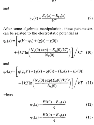
and Fl,? is the Fermi-Dirac integral of order one-half with
and
After some algebraic manipulation, these parameters can be related to the electrostatic potential as
where
are the quasi-Fermi potentials for the electrons and
holes, respectively. It should be noted here that quasi-
equilibrium condition is applied at x = O . Thus, by
convention, we have EFp(0) = EFn(0)=E!(O) (assuming
p-type material here).
Using Equations (2)-(6) we obtain the intrinsic
energy level
It is apparent from (14) that E , ( x ) is not, in general, parallel to V(x) as it is in a uniform non-degenerate
semiconductor. Indeed, El is a purely thermodynamic
property of the intrinsic bulk semiconductors as shown
by Chang [16]. Thus, one cannot use it to align the
energy levels in the energy band diagram.
3. Poisson’s equation
To obtain the electrostatic potential within a heavily
doped semiconductor device we must solve Poisson’s
equation [ 171 with appropriate boundary conditions.
For convenience, consider a one-dimensional p-n junc-
tion with Ohmic contacts at x = O on the p-side and
K M Chang
x = W on the n-side, and with the junction at x , . The Poisson's equation is given by
where K is the dopant density-dependent dielectric
constant, q l is the permittivity in vacuum, and N + =
N : - N , is the ionised dopant density. The carrier
concentrations, p and n, can be expressed in terms of
the electrostatic potential. Algebraic manipulation of
equations (4), ( 9 , (6) and (14), with quasi-equilibrium condition at x = 0 and the reference electrostatic poten- tial
gives the following carrier densities
and
where
AE,= (E,(O) - E g @ ) )
+
kTln(::i;;:$;)
and
( ~ ( x )
-
~ ( 0 ) )+
k T In+
kTIn( C c ( x ) ) ] i A E , . (19) As shown in figure 1, we choose x = 0 as the refer- ence position for the electrostatic potential at which the material is uniform. Also, the actual band-gap narrow- ing effect (ABGN = EG(0) - & ( x ) ) is generally greater than the degeneracy effect (AFD= k T ln(<&)<"(x))).So, both AE, and A are positive quantities. AE, is
called the effective band-gap shrinkage and accounts
for the actual band-gap narrowing effect ( A B G N ) , the
density-of-state effects (ADos), and the influence of
Fermi-Dirac statistics ( A F D ) . A , called the effective
asymmetry factor [18], measures the fraction of the
reduction in band gap that occurs in the conduction
band, 0 SA S 1. In a lightly doped material with
uniform band structure, AEg and A are zero. These
extra terms over conventional results are due to the
non-ideal behaviour of the carriers and can be related to the activity coefficients of the carriers [16].
Assuming that the potential of the Ohmic contacts remains in equilibrium, we obtain the electrostatic potential V ( W ) from (16) as
4 V W ) = S V n ( W
where subscript 0 represents the equilibrium value. In
n-type semiconductors, where NA( W ) = 0, rill( W ) %
po( W ) and one can neglect po( W ) and NA(W) in the charge neutrality condition to yield no( W )
=
ND( W ) . Also, from (14), (P"( W ) is given byq 9 n ( W )
Et(o)
-
E F n ( W )= EP(0) - E ; ( W ) = -qvi, (21) where V, represents the terminal voltage. Again, note
that quasi-equilibrium condition at contact x = W gives
E,,(") = EF,(W)=EF(W). It is the well known result that the separation of the majority quasi-Fermi levels across the entire device is given by the terminal voltage.
The electrostatic potential difference V, across the
entire device is given by
v,
= V( W ) - V(0). (22)Substituting (20), (21) and
into (22) gives
- kTln( <"(O)> -qv;,. (23) It is also noted that the built-in potential Vhl of the junction for the degenerate case is given by [l91 qvbi= -A,(W)AE,,(W)+kTln
(
ND,,,,,,o')- k T W < " ( o ) ) . Substituting (24) into ( 2 3 ) , we have
v,
=v,,
-v;,.
Equation (25) gives the total voltage across the junction
from x = 0 on the p side to x = W on the n side. In equilibrium V, = O and Vbi is given by (24), but if an external voltage V, is applied it changes V,. It is import- ant to note that, for a given bias, Vt becomes smaller as
either A,(") or AE,,(W) becomes larger. The refer-
ence electrostatic potential V(0) and equation (20) can be served as two explicit boundary conditions for solv- ing the Poisson equation.
4. A consistent formulation
In this section, equations presented earlier are used to
Carrier transport in heavily doped semiconductor devices
parameters and thermodynamic quantities, for exam- ple, the reference state chemical potentials and activity coefficients of the carriers which appear in the electro-
chemical potentials of the carriers. The electrochemical
potential ( , L i ) , or quasi-Fermi level, of a charged spe-
cies i in phase a is defined as the sum of its chemical potential and its electric potential energy [20]
,
L
:
= p ;+
ziqVrl=pI*.a+
k T ln(y7c:')+
z,qV" (26) where p: is the chemical potential, p:." is the reference state chemical potential and is a function only of tem-perature, pressure, and choice of reference state, yr is
the activity coefficient, c? is the concentration (ci = n for electrons; c i = p for holes), and
zi
( z i = 1 for holes; 2, = - 1 for electrons) is the elemental charge of speciesi. The potential V" is the electrostatic potential which is
obtained through integration of Poisson's equation
For electrons ( i = n), equating ,Ln = E F , , we have (15).
E F , =,L, = p :
+
k T In(ny,)-
q v . (27)Here we have dropped the superscripts because (27)
holds on either the n-side or p-side. It is clear that we
have two reference states in (27), i.e., p : and qV(0).
This implies that we have two unknowns and only one equation. To get the consistent results, these two refer- ence states cannot be chosen independently. When one is specified, the other must be fixed. In a similar
manner, for holes ( i = p), equation ,Lp =
-
E F p gives-
EFp=pp=pp*
+
kTln (py,) + q v . (28)Note that negative quasi-Fermi energy is used in equa- tion (28). This is because a hole has a charge opposite that of an electron.
Chang [21] has recently addressed the calculation of the reference state chemical potentials and the activity coefficients of the carriers with three different choices of reference for the electrostatic potentials. In the case of
qV(0) = k T In
(c";WoQ)
the results of his analysis for electrons and holes are p:( T) = E,(O)
-
k T In(ni(0))+
q V ( 0 ) (29)p;( T) = - E,(O) - k T In(ni(0))
-
q V ( 0 ) (30)and
y , ( T , p , x ) = e x p ( (32)
where AEg and A are defined by (18) and (19), respecti-
vely. These values combined with (15) and (26) can be
used in the self-consistent result calculations. It is seen from figure 1 that the value of the reference electro- static potential at x = 0 can be arbitrarily chosen
because the field-free vacuum level E,, is an arbitrary one. The choice of
q V ( 0 ) = kTln
(5";;;oy
(a particular value), however, results in the simple
equations (29) through (32) and also leads to a simple
form of Poisson's equation [19]. This choice will be
used henceforth.
5. Transport equations
The electron and hole current densities under isother- mal conditions are given by
J , = n U,V E F n (33) and
JP = p UpV EFp (34)
where U , and Up are the mobilities of electrons and
holes, respectively. The validity of these equations for materials with position-dependent band structures has been established by Marshak and van Vliet [12,22].
If the definition of EF,, (27), is used, the gradient of the electron quasi-Fermi level can be expressed as
V E F n =
-
qVV+ kTV In n+
kTV In y,. (35)Note that
Vu,*
is zero because the reference statechemical potential is a function only of temperature,
pressure and the choice of the reference state.
Substituting (35) into (33) yields
J , = kTU,Vn - qnU,VV+ kTnU,V In yn. (36)
Furthermore, substituting (31) into (36), followed by
some algebraic manipulation, gives
J,=kTU,Vn-qnU,V(V+AAEdq). (37) The hole current density is derived in a similar manner. For holes, an expression for the gradient of the quasi- Fermi level can be obtained by using the definition of E F p in (28). The result for E F p is
V E F p =
-
qVV- kTV l n p - kTV In yp. (38)Again, we use the fact that
V&
= O . Substituting (38) into (34), we obtainJ p = - k T U p V p - q p U p V V - k T p U p V I n y p . (39)
Equation (39) can be rewritten in terms of AEg and A .
Using (32) in the last term of (39) and rearranging yields
Jp=-kTUpVp-qpUpV V - ( l - A ) L
i
.
(40)AE 4
1
Equations (37) and (40) or (36) and (39) are convenient to use in semiconductor device analysis. Althoughthese equations are expressed in a simple form, they
correctly describe carrier transport in materials with a
K M Chang
position-dependent band structure. The effects of the
non-uniform band structure and the carrier degeneracy
are described by two parameters, AEg and A , which are
expressed in terms of the carrier activity coefficients.
The results presented here are identical in form to
those derived by Marshak and van Vliet [22]. The
treatments, however, are different. These results along with those discussed in [22] would give a good descrip-
tion of the carrier transport in degenerate materials
with non-uniform band structure.
6. The pn product
The carrier concentrations given by equations (16) and (17) can be related to their activity coefficients by (31) and (32) as
and
It is noted that the pre-exponential factor in equations
(41) and (42) has the same value only if band-gap
narrowing is symmetric (i.e., A = or yn = yp), which
rarely occurs [23]. Even as the carrier is non-degener-
ate, asymmetric band-gap narrowing gives different
pre-exponential factors in (41) and (42). This is
contrary to the results of [8].
From (41) and (42), the p n product is then given by
where the y n y p product, from (31) and (32), is given by
We define an effective intrinsic carrier concentration as the pn product in equilibrium (EFn = EFp) [ l , 11, 131; thus
where the subscript zero denotes equilibrium.
Substituting (45) into (43) gives the p n product for all cases
These equations can be simplified for special cases of
interest. As an example, for non-degenerate uniform
semiconductors (yn = ynll = y p = ypl, = l ) , equations (41), (42) and (46) reduce to
and
p ( x ) n ( x ) = n:(O) exp
(EFni3
(49)In the case of low-level injecton, i.e. y n = y n l j and yp=ypl,
or A€,= AE,,,, (46) reduces to
This result can be used for all practical conditions (even for high-level injection) in Si.
7. Discussion
7.1. The choice of reference states
The choice of the reference states is quite arbitrary. The proper choice, however, of these reference states
can lead to simpler working equations for the
problems. For example, we choose x=x,- as the refer-
ence position for the electrostatic potential at which
q V ( x j ) = O . The results for the carrier concentrations and the potential at the contacts are given by
n ( x ) = n ( x ; ) exp ( q ( V ( x )
-
qn(x))+
AAE, k TCarrier transport in heavily doped semiconductor devices
The parameters A E , and A in equations (51)-(54) are defined by equations (57) and ( 5 8 ) as
and
+ k T l n ( C o j l / h E , . I;c(x,) (58) Note that the parameters A E g and A given by (57) and
( 5 8 ) are different from those defined by (18) and (19)
due to two different choices of the reference states. It is
also noted that the pre-exponential factors in (51) and
(52) are different from those given by (16) and (17). It is clear that the boundary conditions for the
integration of Poisson's equation are explicit for the
case of
q V ( 0 ) = k T In
( C " y o Q )
(discussed previously), while they are implicit for
q V ( x ; )
=0
due to the unknown quantities p(x,-) andn ( x ; ) . Therefore, the numerical computation for solv-
ing the Poisson equation is quite straightforward for the former case.
7.2. Alternative current equations
In a typical analysis, the electric field is expressed in terms of the electrostatic potential as
E = -VV. (59) Using (59) in (36) and (39), we obtain the current equation, which is rewritten in terms of E
J , = k T U , V n f q n U , E + k T n U , V I n yn (60) and
J , = - kTU,Vp
+
qpU,E - kTpU,V In yp. (61)In this form, only one parameter, i.e. the activity
coefficient, is necessary to describe the effect of the
non-uniform band structure and the influence of the
Fermi-Dirac statistics. The current density, via its
dependence on y,, in (60) and y p in (61), depends not
only on the effective band-gap narrowing but also on
the effective asymmetry in band-gap narrowing. It is
important to note that the diffusivity is not needed to
evaluate (60) and (61) because the coefficient in front
of the diffusion terms involves only the mobility, which can be obtained from experiment.
7.3. Minority-carrier current and concentration
In order to solve for the steady-state minority carrier concentration, for example p in a heavily doped n-type region in low injection, we return to (40). It should be useful to define the effective electric field in analysis as
JP = - kTU,Vp
+
qp U,E, (62) whereThe 'effective' electric field (electric plus quasi-electric) E , can be evaluated by equating (62) to zero for thermal equilibrium conditions
For low-injection conditions, E, is not altered from its equilibrium value given by (62) [18]. Combining (45) and (64) yields
Here we assume n,,= N D . Substituting (65) into (62)
gives
Equation (66) shows that the minority carrier current density is evaluated independently of how A is chosen.
Equation (66) is inserted into the steady-state hole continuity equation:
V . J , + q ( R - G ) = O (67) where R , the recombination rate of carriers and G , the
rate at which they generate, are assumed to be inde-
pendent of the effective asymmetry factor. When two boundary conditions on p are specified, (67) can be solved for the steady-state hole density. The boundary condition at the contact W can be either a Dirichlet type or a Neumann type. The second boundary con- dition at the edge of the space charge region follows from the non-equilibrium form of (50)
where V i , represents the portion of the applied voltage
that appears across the junction. Equation (68) indi-
cates that the relationship between the junction poten- tial and the minority carrier density at the edge of the
K M Chang
space charge region is obtained regardless of the choice of A in the transport equations.
The discussion presented above shows that the car- rier concentrations and minority carrier current density
of heavily doped semiconductor device are correctly
modelled even when the choice for A in (37) and (40) is
made arbitrarily. However, the electrostatic potential, built-in potential and chemical potential cannot be evaluated unless A is known. These quantities depend
strongly on the A-value. These results are also
observed when the semiconductor equations for a
Gaussian p-n junction are solved numerically [24].
8. Conclusions
In this paper we present a self-consistent formulation for the thermodynamic quantities, the transport equa- tions, the steady-state continuity equations and the
electrostatic potential with explicit boundary conditions at the contacts. The formulation of the model requires the selection of reference for the electrostatic potential
and the evaluation of the activity coefficients of the
carriers. Special emphasis has been placed on writing the working equations in a simple form by the proper choice of the reference states. These general transport
equations, which are similar to those derived by
Marshak and van Vliet [13, 221, were obtained from a
simple but general thermodynamic point of view and
written in a simple form for use in device analysis. In this form, the effects of the non-uniform band structure and the influence of Fermi-Dirac statistics are described by one thermodynamic quantity, the activity coefficient of the carriers, which is expressed in terms
of two energy band model parameters, the effective
band-gap shrinkage, A E g , and the effective asymmetry
factor, A . These parameters correctly account for the changes in the band structure and the carrier degener-
acy which occur in regions that are heavily doped.
When experimentally measured heavy-doping para-
meters are used in the simple Shockley-like transport equations, no further correction for degenerate statis- tics is necessary. Finally, it was shown, in the case of low injection, that the carrier densities and the minority
carrier current density in semiconductor devices with
quasi-neutral, heavily doped regions, can be modelled accurately, independently of the choice of A .
Acknowledgments
Support of this work by the ROC National Science
Council, Engineering Division under Grant
NSC77-0404-009-13 is gratefully acknowledged. The author is indebted to an anonymous referee for a
careful reading and criticism of the manuscript.
References
[ l ] Lindholm F A and Sah C T 1977 IEEE Trans. [2] Slotboom J W and de Graaff H C 1976 Solid-state [3] Lanyon H P D and Tuft R A 1979 IEEE Trans. [4] Blakemore J S 1962 Semiconductor Statistics (New [5] Abram R A, Rees G J and Wilson B L H 1978 A d o . [6] Tanenbaum M and Thomas D E 1956 Bell Syst. [7] De Man H J J 1971 IEEE Trans. Electron Devices [8] Adler M S 1978 Tech. Digest IEDM Washington 550 [9] Lawers P, van Meerbergen J , Bulteel P, Mertens R
and van Overstraeten R 1978 Solid-State Electron.
16 1251
Electron Devices ED-24 299 Electron. 19 857
Electron Devices ED-26 1014
York: Pergamon)
Phys. 27 799 Tech. J. 35 1 ED-l8 833
[lo] Mock M S 1973 Solid-State Electron. 21 747 [l11 van Overstraeten R J , DeMan H J and Mertens R P
1973 IEEE Trans. Electron Devices ED-20 290 [l21 Marshak A H and van Vliet K M 1978 Solid-State
Electron. 21 417
[l31 Marshak A H and van Vliet K M 1978 Solid-State
Electron. 21 429
[l41 van Vliet K M and Marshak A H 1980 Solid-state
Electron. 23 49
[l51 Lundstrom M S, Schwartz R J and Gray J L 1981
Solid-state Electron. 24 195
[l61 Chang K M 1988 J . Electrochem. Soc. submitted for publication
[l71 Sze S M 1981 Physics of Semiconductor Devices (New York: Wiley)
[l81 Shibib M A 1979 PhD disseratation University of Florida, Gainesville
[l91 Chang K M 1988 Solid-State Electron. submitted for publication
[20] Haase R 1969 in Thermodynamics of Irreversible Processes (California: Addison-Wesley)
[21] Chang K M 1988 J . Electrochem. Soc. submitted for publication
[22] Marshak A H and van Vliet C M 1984 Proc. I E E E 72 148
[23] Wilson B L H 1977 Solid-state Electron. 20 71 [24] Chang K M 1988 E D M S Taiwan ROC submitted for