Crack-free Ga N Al N distributed Bragg reflectors incorporated with Ga N Al N
superlattices grown by metalorganic chemical vapor deposition
G. S. Huang, T. C. Lu, H. H. Yao, H. C. Kuo, S. C. Wang, Chih-Wei Lin, and Li Chang
Citation: Applied Physics Letters 88, 061904 (2006); doi: 10.1063/1.2172007
View online: http://dx.doi.org/10.1063/1.2172007
View Table of Contents: http://scitation.aip.org/content/aip/journal/apl/88/6?ver=pdfcov Published by the AIP Publishing
Articles you may be interested in
Strain-compensated Al Ga N Ga N In Ga N cladding layers in homoepitaxial nitride devices Appl. Phys. Lett. 91, 231914 (2007); 10.1063/1.2823587
Cr N x and Cr 1 x Al x N as template films for the growth of -alumina using ac reactive magnetron sputtering J. Vac. Sci. Technol. A 25, 1367 (2007); 10.1116/1.2756542
In situ pendeoepitaxy of GaN using heteroepitaxial Al Ga N Ga N cracks Appl. Phys. Lett. 89, 024103 (2006); 10.1063/1.2219093
Crack-free fully epitaxial nitride microcavity with Al GaN GaN distributed Bragg reflectors and InGaN GaN quantum wells
Appl. Phys. Lett. 88, 191111 (2006); 10.1063/1.2202702
Relaxation mechanisms in metal-organic vapor phase epitaxy grown Al-rich ( Al , Ga ) N Ga N heterostructures J. Appl. Phys. 97, 024912 (2005); 10.1063/1.1828607
This article is copyrighted as indicated in the article. Reuse of AIP content is subject to the terms at: http://scitation.aip.org/termsconditions. Downloaded to IP: 140.113.38.11 On: Thu, 01 May 2014 02:08:40
Crack-free GaN / AlN distributed Bragg reflectors incorporated with
GaN / AlN superlattices grown by metalorganic chemical vapor deposition
G. S. Huang, T. C. Lu, H. H. Yao, H. C. Kuo, and S. C. Wanga兲Department of Photonics & Institute of Electro-Optical Engineering, National Chiao Tung University, 1001 TA Hsueh Road, Hsinchu, Taiwan, 300 Republic of China
Chih-Wei Lin and Li Chang
Department of Materials Science and Engineering, National Chiao Tung University, 1001 TA Hsueh Road, Hsinchu, Taiwan, 300 Republic of China
共Received 31 August 2005; accepted 16 December 2005; published online 7 February 2006兲 A crack-free GaN / AlN distributed Bragg reflector共DBR兲 incorporated with GaN/AlN superlattice 共SL兲 layers was grown on a c-plane sapphire substrate by metalorganic chemical vapor deposition. Three sets of half-wave layers consisting of 5.5 periods of GaN / AlN SL layers and GaN layer were inserted in every five pairs of the 20 pair GaN / AlN DBR structure to suppress the crack generation. The grown GaN / AlN DBRs with SL insertion layers showed no observable cracks in the structure and achieved high peak reflectivity of 97% at 399 nm with a stop band width of 14 nm. Based on the x-ray analysis, the reduction in the in-plane tensile stress in the DBR structure with insertion of SL layers could be responsible for the suppression of crack formation and achievement of high reflectivity. © 2006 American Institute of Physics. 关DOI:10.1063/1.2172007兴
GaN-based vertical cavity surface emitting lasers 共VCSELs兲 have attracted great interest for various optical applications.1 Highly reflective epitaxial distributed Bragg reflectors共DBRs兲, such as quarter-wave GaN/AlGaN multi-layers, have played an important role in the operation of VCSELs.2,3 Because of the relatively high contrast of the refractive index between GaN and AlN in comparison to the GaN / AlGaN DBRs, a small number of GaN / AlN DBR pairs is required to achieve a high reflectivity with a broad stop band width. However, the large lattice mismatch be-tween GaN and AlN induces a lot of cracks in the DBR when the number of the epitaxial pairs increases. These cracks tend to grow into V-shaped grooves, which seriously affect the reflectivity of the DBR due to scattering, diffraction and ab-sorption. Therefore, it is necessary to suppress crack genera-tion to achieve a smooth surface and a high reflectivity. Shirasawa and our group have studied and reported a metal-organic chemical vapor deposition 共MOCVD兲 grown GaN / AlN DBRs.4,5Ng, Moustakas, and Chu reported a mo-lecular beam epitaxy grown GaN / AlN DBR with a reflec-tivity of 99%.3 However, these samples exhibited extensive cracking surfaces. Many research groups have studied and reported the approaches of using GaN / AlGaN or AlN / AlGaN superlattice共SL兲 insertion layers to reduce the biaxial tensile strain and successfully suppress crack genera-tion while growing high Al-contained structures.6–10Nakada
et al. have reported a MOCVD grown 30-pair GaN / Al0.41Ga0.59N DBR with a reflectivity of 98%. They
employed 100 periods of GaN / AlGaN SL insertion layers prior to the growth of the GaN / AlGaN DBRs to decrease the tensile strain in the DBRs.6 In this letter, we report the growth of the crack-free 20-pair GaN / AlN DBRs with inser-tion of three sets of 5.5 periods of GaN / AlN SL during the growth and the achievement of high reflectivity with wide stop band width.
The GaN / AlN DBRs were grown in a low pressure EMCORE D75 MOCVD system. 共0001兲-oriented, 2-in.-diam sapphire substrates were used for the growth of samples. Trimethylgallium and trimethylaluminum were used as group III source materials and ammonia as the group V source material. The growth pressure was kept at 100 Torr. The surface morphology of the DBRs was studied by the optical microscope. The thicknesses of the individual layers in the DBRs were investigated by transmission elec-tronic microscopy 共TEM兲. Measurements on the reciprocal space maps 共RSMs兲 of x-ray diffraction intensity were per-formed on the Philips X’Pert material research diffraction system around an asymmetrical GaN 共101¯5兲 Bragg peak. The reflectivity spectrum of the GaN / AlN DBRs was mea-sured by the n & k ultraviolet-visible spectrometer with nor-mal incidence at room temperature.
Figure 1 shows two DBR layer structures grown and examined in this study. The normal DBR structure without the SL layers referred to as the non-SL sample was grown for
a兲Author to whom correspondence should be addressed; electronic mail:
FIG. 1. Structures of the non-SL and SL samples grown and examined in this study. Non-SL sample is the normal 20-pair GaN / AlN DBR and the SL sample has been inserted with three sets of 5.5 periods of GaN / AlN SL in the 20-pair GaN / AlN DBR.
APPLIED PHYSICS LETTERS 88, 061904共2006兲
0003-6951/2006/88共6兲/061904/3/$23.00 88, 061904-1 © 2006 American Institute of Physics
This article is copyrighted as indicated in the article. Reuse of AIP content is subject to the terms at: http://scitation.aip.org/termsconditions. Downloaded to IP: 140.113.38.11 On: Thu, 01 May 2014 02:08:40
comparisons. The non-SL DBR sample has the following layers: a 30-nm-thick GaN nucleation layer grown at 500 ° C, a 2-m-thick GaN bulk layer grown at 1100 ° C, and 20 pairs of quarter-wave GaN / AlN layers grown at 1100 ° C. The ambient gas was changed from hydrogen into nitrogen before the DBR layers were grown. For the DBR structure with SL layers, referred to as the SL sample, three sets of a half-wave layer consisting of 5.5 periods of GaN / AlN SL and GaN layer were inserted in every five pairs of the 20-pair GaN / AlN DBR structure, while keeping the other growth conditions the same as the non-SL sample. The center wavelength of these DBRs was designed to be around 400 nm.
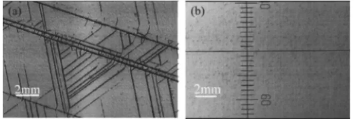
Figure 2 shows the optical microscopy image of these two samples. For the non-SL sample, cracks were always observed when the number of DBR pairs is greater than 10 关Fig. 2共a兲兴. However, the cracks were not observed in our case when the number of DBR pairs is less than 5. As a result, we chose to insert three sets of a half-wave layer consisting of a quarter-wave GaN / AlN SL and a GaN layer in every five pairs of GaN / AlN DBRs in the SL sample. No cracks were observed for the SL sample as shown in Fig. 2共b兲.
Figure 3 shows cross-sectional TEM images of the SL sample. The lighter layers represent AlN layers while the darker layers represent GaN layers. In Fig. 3共a兲, no cracks can be observed in the TEM image. However, some V-shaped defects共dark spots兲 were still observed on the in-terfaces of GaN or AlN layers in Fig. 3共a兲. These V-shaped defects have been reported earlier to be due to various ori-gins such as stacking mismatch boundaries and surface undulation.11 Figure 3共b兲 shows the cross section of one set of 5.5 pairs of GaN / AlN SL insertion layers. The interface between GaN and AlN is sharp and abrupt. The GaN / AlN
SL insertion layers were ended by one more AlN layer to identify the interface changing from the AlN layer to the GaN layer. Here a set of GaN / AlN SL insertion layers can be seen as a digital alloy of an AlxGa1−xN layer共x⬃0.5兲 for
a low reflective index quarter-wave layer in the DBR struc-ture because the wavelength of light being reflected was much longer 共⬃400 nm兲 than the thicknesses of AlN and GaN layers共⬃3–5 nm兲 in SL.
The effect of the SL insertion layers on the structural characteristics of these DBR samples was investigated based on the asymmetrical RSMs. Figures 4共a兲 and 4共b兲 show the 共101¯5兲 RSMs of the non-SL and SL samples. The perpen-dicular axis represents the reciprocal lattice c and the parallel axis represents reciprocal lattice a. The growth direction and in-plane strains of the epilayer can be calculated by the dis-tances along two axes from the GaN reciprocal lattice point, respectively. The in-plane strain xx for the epitaxial layer
grown on GaN layer can be calculated from qxGaN/ qxEpi− 1,
where qx GaN
and qx Epi
are the x positions of the GaN and the epitaxial layer to be determined, respectively. Compared with the RSM patterns of non-SL and SL samples in Figs. 4共a兲 and 4共b兲, the diffraction pattern around spots labeled A and B are due to the DBR layers for the high aluminum composition. In Fig. 4共b兲, the diffraction spot labeled C is due to the SL insertion layers. Both RSM patterns in non-SL and SL samples indicate that the DBR layers are under the tensile strain and the tensile strain is partially relaxed be-cause the diffraction peaks do not align in a vertical straight line. The relaxation could be due to the creation of the misfit dislocation.11The biaxial tensile strain in AlN layer relative to GaN layer in non-SL sample is large共about 0.013 in xx兲
thus the accumulation of this stress can lead to generation of cracks. However, the in-plane strain of spot A relative to that of spot C of the SL layers in the SL sample is 0.008, which is much smaller than the tensile strain of spot A 共0.013兲 relative to the GaN bulk layer underlying the DBR layers in the non-SL sample. Based on these data the insertion of the SL layers during the growth of the DBR layers could act as strain buffers between DBRs and the underlying GaN bulk layer because the in-plane lattice constants of the SL layers are close to those of the AlN layers in the DBRs. As a result, the relative tensile stress in the AlN layers in the DBRs is reduced and the crack generation could be suppressed.
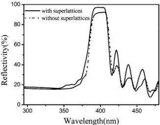
Figure 5 shows reflectivity spectra of two samples. They exhibit flattop stop bands, indicating high crystal quality of FIG. 2. Plane-view optical microscope images of the 20 periods of
GaN / AlN DBRs for共a兲 non-SL sample and 共b兲 SL sample.
FIG. 3. TEM cross-sectional image of the SL sample for共a兲 top 17 pairs of DBR structure, and共b兲 one set of AlN/GaN SL.
FIG. 4. Reciprocal space maps of共a兲 non-SL and 共b兲 SL samples.
061904-2 Huang et al. Appl. Phys. Lett. 88, 061904共2006兲
This article is copyrighted as indicated in the article. Reuse of AIP content is subject to the terms at: http://scitation.aip.org/termsconditions. Downloaded to IP: 140.113.38.11 On: Thu, 01 May 2014 02:08:40
the samples. The peak reflectivity of the SL sample at 399 nm is 97%, and the stop band width is 14 nm. However, the peak reflectivity of the non-SL sample at 400 nm is only 92%, and the stop band width is 13 nm. The reduction of the cracks should be an important factor in obtaining a high reflectivity of SL sample.
In conclusion, we have fabricated and characterized a crack-free 20-pair GaN / AlN DBRs with the SL insertion layers. The DBR showed no observable cracks and high re-flectivity of 97% compared to the 92% rere-flectivity of non-SL DBR samples. The stop band width was also increased from 13 to 14 nm. The RSM analysis indicated the reduction in
the in-plane tensile stress in the SL sample that could be responsible for the crack suppression and improvement in the reflectivity of the SL DBRs. This technique should be applicable for the fabrication of GaN-based VCSELs requir-ing high reflectivity and broad stop band width AlN / GaN DBRs.
This work was supported in part by the National Science Council of the Republic of China 共ROC兲 in Taiwan under Contract No. NSC93-2120-M-009-006 and by the Academic Excellence Program of the ROC Ministry of Education under Contract No. NSC93-2752-E-009-008-PAE.
1S. Nakamura, M. Senoh, S. Nagahama, N. Iwasa, T. Yamada, T.
Matsushita, Y. Sugimoto, and H. Kiyoku, Appl. Phys. Lett. 69, 1477 共1996兲.
2T. Honda, A. Katsuhbe, T. Sakaguchi, F. Koyama, and K. Iga, Jpn. J. Appl.
Phys., Part 1 34, 3527共1995兲.
3H. M. Ng, T. D. Moustakas, and S. N. G. Chu, Appl. Phys. Lett. 76, 2818
共2000兲.
4T. Shirasawa, N. Mochina, A. Inoue, T. Honda, T. Sakaguchi, F. Koyama,
and K. Iga, J. Cryst. Growth 189/190, 124共1998兲.
5H. H. Yao, C. F. Lin, H. C. Kuo, and S. C. Wang, J. Cryst. Growth 262,
151共2004兲.
6N. Nakada, H. Ishikawa, T. Egawa, and T. Jimbo, Jpn. J. Appl. Phys., Part
2 42, L144共2003兲.
7J. P. Zhang, H. M. Wang, M. E. Gaevski, C. Q. Chen, Q. Fareed, J. W.
Yang, G. Simin, and M. Asif Khan, Appl. Phys. Lett. 80, 3542共2002兲.
8E. Feltin, B. Beaumont, M. Laugt, P. Vennegues, H. Lahreche, M. Leroux,
and P. Gibart, Appl. Phys. Lett. 79, 3230共2001兲.
9M. Kurimoto, T. Nakada, Y. Ishihara, M. Shibata, T. Honda, and H.
Kawanishi, Jpn. J. Appl. Phys., Part 2 38, L552共1999兲.
10Y. Ishihara, J. Yamamoto, M. Kurimoto, T. Takano, T. Honda, and H.
Kawanishi, Jpn. J. Appl. Phys., Part 2 38, L1296共1999兲.
11H. K. Cho, J. Y. Lee, and G. M. Yang, Appl. Phys. Lett. 80, 1370共2002兲.
FIG. 5. Reflectivity spectra of 20-pair DBRs of共a兲 non-SL and 共b兲 SL samples.
061904-3 Huang et al. Appl. Phys. Lett. 88, 061904共2006兲
This article is copyrighted as indicated in the article. Reuse of AIP content is subject to the terms at: http://scitation.aip.org/termsconditions. Downloaded to IP: 140.113.38.11 On: Thu, 01 May 2014 02:08:40