Effects of Al x Ga 1 x N interlayer for GaN epilayer grown on Si substrate by
metal-organic chemical-vapor deposition
Kung-Liang Lin, Edward-Yi Chang, Yu-Lin Hsiao, Wei-Ching Huang, Tien-Tung Luong, Yuen-Yee Wong, Tingkai Li, Doug Tweet, and Chen-Hao Chiang
Citation: Journal of Vacuum Science & Technology B 28, 473 (2010); doi: 10.1116/1.3385672 View online: http://dx.doi.org/10.1116/1.3385672
View Table of Contents: http://scitation.aip.org/content/avs/journal/jvstb/28/3?ver=pdfcov Published by the AVS: Science & Technology of Materials, Interfaces, and Processing
Articles you may be interested in
Magnetostrictive effect in single crystal Fe 1 x Ga x thin films J. Appl. Phys. 107, 09A924 (2010); 10.1063/1.3367971
Comparison of electrical properties and deep traps in p -Al x Ga 1 x N grown by molecular beam epitaxy and metal organic chemical vapor deposition
J. Appl. Phys. 106, 073706 (2009); 10.1063/1.3238508
Semitransparent inverted polymer solar cells with MoO 3 / Ag / MoO 3 as transparent electrode Appl. Phys. Lett. 95, 053303 (2009); 10.1063/1.3196763
Properties of single crystal Fe 1 x Ga x thin films J. Appl. Phys. 105, 07A938 (2009); 10.1063/1.3077207
Growth of strained Si on high-quality relaxed Si 1 x Ge x with an intermediate Si 1 y C y layer J. Vac. Sci. Technol. A 23, 1141 (2005); 10.1116/1.1913679
low-pressure metal-organic chemical-vapor deposition method. The AlxGa1−xN films with Al
composition varying from 1 to 0.66 were used to accommodate the stress induced between GaN and the Si substrate during GaN growth. The correlation of the Al composition in the AlxGa1−xN films
with respect to the stress induced in the GaN film grown was studied using high-resolution x-ray diffraction, including symmetrical and asymmetrical/2 scans and reciprocal space maps. It is found that with proper design of the Al composition in the AlxGa1−xN buffer layer, crack-free GaN
film can be successfully grown on 6 in. Si 共111兲 substrates using multilayer AlN and AlxGa1−xN
buffer layers. © 2010 American Vacuum Society. 关DOI: 10.1116/1.3385672兴
I. INTRODUCTION
Growth of GaN on Si共111兲 is of particular interest to the compound semiconductor industry due to lower cost and larger area, in comparison with other substrates and the pos-sibility of integrating conventional Si-based devices with group III nitride devices on a single wafer. Due to the con-siderable differences in lattice parameters and thermal-expansion coefficients 共CTEs兲 between GaN and Si sub-strates, the growth of high-quality, crack-free GaN films on a Si substrate poses serious difficulties. Thus, strain is an im-portant issue for the growth of group III nitride growth on Si to achieve GaN-based devices, such as light-emitting diodes and field-effect transistors on a Si substrate. Therefore, a reduction in the stress and cracking in the GaN film is re-quired for the growth of GaN on the Si共111兲 substrate. To obtain high-quality GaN film on Si substrates, the design of the interlayer structure between the GaN and the Si substrate is important. Using a low temperature AlN 共LT-AlN兲 inter-layer contributes to the reduction in the growth stress.1–6 However, the quality of the AlN film grown at low tempera-ture is inferior to the AlN grown at high temperatempera-ture because of the formation of dislocations, especially the edge-threading dislocation共TD兲, at low temperatures, which influ-ences the quality of the GaN film grown. On the other hand, due to the significant lattice mismatch between AlN and Si, cracks and higher defect density are formed on the AlN ep-ilayer when it is grown at high temperature共1100 °C兲. Fur-thermore, compressive stress共about 9 GPa兲 is generated on GaN epitaxially grown on high-quality AlN due to the lattice mismatch between AlN and GaN.7In this case, an AlxGa1−xN
intermediate buffer should be used to reduce the lattice
mis-match between GaN and AlN.8In this article, we report the properties of the GaN layer grown on a Si 共111兲 substrate with a composite buffer, including a AlxGa1−xN interlayer
with fixed Al composition共x was set at a fixed value between 0.5 and 0.25兲, a graded AlxGa1−xN layer共x varies from 1 to
0.66兲, and a multilayer AlN grown by the metal-organic chemical-vapor deposition 共MOCVD兲 system. It is found that the composite buffer can greatly reduce the cracks and improve the crystal quality of the GaN layer grown and thus improve the structural and optical properties of the GaN layer.
II. EXPERIMENT
The multilayer AlN, the AlxGa1−xN layers, and the GaN
film were grown by an EMCORE D-180 MOCVD reactor on a 6 –in. Si 共111兲 wafer. The substrate resistivity, thickness, and warp were 7 – 13 ⍀ cm, 675 m, and ⬍30 m, re-spectively. These wafers were Czochralski wafers with a single side polished. The trimethyl gallium 共TMGa兲, trim-ethyl aluminum 共TMAl兲, and ammonia 共NH3兲 were the
source gases for Ga, Al, and N, respectively. H2was used as the carrier gas. The substrates were first degreased using a H2SO4: H2O2: H2O 共3:1:1兲 solution for 5 min, then etched
with HF 共2%兲 for 1 min to remove the surface oxide layer before the epitaxial growth.9After that, the Si共111兲 substrate was heated in the MOCVD reactor under H2 ambient at
1050 ° C for 10 min prior to growth to remove the surface oxide thermally. Before introducing NH3into the reactor, Al
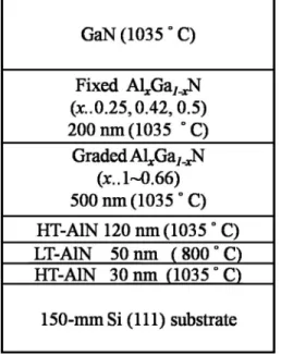
was predeposited for 10 s on Si substrate to prevent the for-mation of SiNx. Figure 1 shows the layer structures of the
samples grown in this study. As shown in TableI, sample A is a reference sample of GaN film grown on the Si 共111兲 substrate with only a multilayer AlN buffer. The growth
tails are as described in the earlier report.10 Samples B–D consist of a multilayer AlN combined with a graded AlxGa1−xN layer and a fixed AlxGa1−xN layer buffer. The
GaN films were then grown on the top of these buffers. To control the Al fraction共x兲 in the fixed AlxGa1−xN interlayer,
different TMGa flow rates of 16.6, 12.2, and 13.8 mol/min with fixed TMAl flow rate of 111.4 mol/min were used for samples B, C, and D, respectively. The growth time of the graded AlxGa1−xN and the fixed composition AlxGa1−xN
layers was set at 40 and 20 min, respectively. The growth temperature of the multilayer AlN was 800 ° C for the 50 nm LT-AlN layer and 1035 ° C for the HT-AlN layers. Mean-while, the growth temperature of the graded AlxGa1−xN
layer, the fixed composition AlxGa1−xN layer, and the GaN
layer were also set at 1035 ° C. The reactor pressures were set at 50, 100, and 300 torr during the growth of the AlN, AlxGa1−xN, and GaN layers, respectively. High-resolution
x-ray diffractometry 共XRD兲, transmission-electron micros-copy共TEM兲, and an optical microscope were used to inves-tigate the composition, structure, cross-sectional image, and the surface morphologies of the films. The stress states in the films were studied using the Raman spectroscopy.
III. RESULTS AND DISCUSSION
Figure2shows the-2 XRD scans of the 0.8 m GaN grown on different types of buffers with AlN multilayers in combination with a composition-graded AlxGa1−xN layer and
a fixed Al composition AlxGa1−xN layer. The detailed buffer
structures of samples A–D are as listed in TableIand Fig.1. In this case, the thicknesses of the graded AlxGa1−xN layer
and the fixed composition AlxGa1−xN layer are 500 and 200
nm, respectively. The Al composition in the AlxGa1−xN
lay-ers was determined from the lattice constant measurement using XRD, assuming that Vegard’s law is obeyed by the AlxGa1−xN films. Figure2 presents the variation in the XRD
2scan for the AlxGa1−xN film with Al composition varying
from 0.5 to 0.25. The rocking curves of the GaN共004兲 and AlN共004兲 plans were also scanned for each sample. The full width at half maximum 共FWHM兲 values of the rocking curves are listed in TableI. For sample D, the FWHMs of the GaN 共004兲 and AlN 共004兲 scans are the smallest. As the Al mole fraction 共x兲 of the fixed composition AlxGa1−xN
in-creases from 0.25 to 0.42, the crystal quality of GaN also improves due to the reduction in the lattice mismatch be-tween GaN and AlN. However, when Al mole fraction is higher than 0.42, the crystallinity of GaN becomes worse. This is because of a considerable amount of misfit strain has been induced due to the large differences in CTE and lattice constant, when the Al concentration is higher than 0.42. This result is in agreement with the reports by Raghavan and Redwing11and Saengkaew et al.12 Therefore, it can be con-FIG. 1. Schematic view of GaN/Si共111兲 with the fixed AlxGa1−xN/graded
AlxGa1−xN/HT-AlN/LT-AlN/HT-AlN buffer.
TABLEI. Layer thickness, composition, and induced strain for samples A–D with different buffers.
Sample GaN thickness 共m兲 AlNa thickness 共nm兲 Graded AlxGa1−xN thickness 共nm兲 Fixed AlxGa1−xN x fraction Fixed AlxGa1−xN thickness 共nm兲 AlN strain 共a兲 AlN XRD 共004兲 FWHM 共deg兲 GaN strain 共a兲 GaN XRD 共004兲 FWHM 共deg兲 A 0.8 200 0 0 0 0.378 0.717 0.146 0.322 B 0.8 200 500 0.25 200 0.335 0.319 0.137 0.228 C 0.8 200 500 0.50 200 0.312 0.357 0.132 0.242 D 0.8 200 500 0.42 200 0.300 0.293 0.120 0.158
aMultilayer AlN共high temperature/low temperature/high temperature AlN兲.
FIG. 2.共Color online兲 XRD-2scan of GaN films grown on various types of multilayer AlN/graded AlxGa1−xN/fixed AlxGa1−xN composition buffers.
474 Lin et al.: Effects of AlxGa1−xN interlayer for GaN epilayer grown on Si substrate by MOCVD 474
cluded that with the Al mole fraction x = 0.42 in the fixed AlxGa1−xN film, the strain induced by the lattice mismatch
between AlxGa1−xN and other films compensates the strains
induced in the GaN and AlN films on the Si substrate. The thermal stress can be calculated from the average value of the CTE of Si and GaN using the following relation:13 =共␣GaN−␣Si兲共Tgrowth− TRT兲, where␣GaNand␣Si
are the CTEs of GaN 共5.59⫻10−6 K−1兲 and Si 共3.59 ⫻10−6 K−1兲, respectively. T
growth and TRT are the growth
temperature 共1035 °C兲 and room temperature 共25 °C兲, re-spectively. The tensile strain of GaN grown on Si after cool-ing down was=0.202%. TableIshows that the strain in the GaN film is smaller than the theoretical nature tensile. This means that AlN and AlxGa1−xN interlayers can reduce the
thermal stress induced during the cooling effectively. Since the Al composition in the AlxGa1−xN layers could
be accurately controlled by the MOCVD growth, a graded AlxGa1−xN interlayer with a total thickness of about 500 nm
was successfully grown on top of the AlN buffer layer to reduce the lattice strain further and improve the GaN prop-erties. Figure 2 shows the 2 XRD scan of the GaN films grown on the multilayer AlN buffer with a graded AlxGa1−xN
interlayer in the samples. As the Al composition in the AlxGa1−xN interlayer was graded, the thermal-expansion
co-efficient of the graded AlxGa1−xN interlayer was gradually
changed from that of AlN to that of GaN. Therefore, the thermal stress may be accommodated within the graded AlxGa1−xN interlayer. It is expected that a complete
elimina-tion of cracks can be achieved through optimizaelimina-tion of the composition and thickness of the graded AlxGa1−xN
inter-layer.
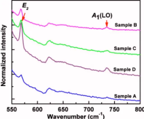
The room-temperature Raman spectra of the E2-high and
A1 共LO兲 line for the samples are presented in Fig. 3. The
spectra show strong E2共TO兲-high and A1共TO兲 modes under
z共x−兲-z scattering geometry. The E2共TO兲 Raman peak is
gen-erally used to estimate the in-plane strain. For samples A–D, the Raman shifts of the E2共TO兲 phonon peaks were 566.8,
566.6, 566.9, and 567.2 cm−1, respectively. The residual
stresses in the samples were calculated from the measured wave number shifts of the E2-high mode in the Raman
spectra.14 The values of the tensile stress in the GaN films
The surfaces of all samples grown were mirrorlike. How-ever, crack lines were found near the wafer edges on samples A–C as observed by optical microscope. Meanwhile, sample D was crack-free, the optical micrograph showing crack-free GaN on Si was reported in an earlier report.10 In this study, the insertion of a graded composition AlxGa1−xN interlayer
and a fixed composition Al0.42Ga0.58N layer has significantly compensated the tensile stress induced in the GaN film grown on Si substrate. The reduction in in-plane tensile stress was further evidenced by the improved crystalline quality of the GaN films in sample D, for which the GaN 共004兲 FWHM was only 0.158 arc sec. In sample D, the wafer bowing was −8.63 m and the radius of curvature was 238.96 m. Photoluminescence mapping was used to evaluate the film quality and film uniformity. The peak wavelength distribution was quite narrow, ranging from 364.5 to 367 nm. The mean value was 365.3 nm with standard deviation of 0.2%.
A second source of stress is the lattice mismatch between the buffer and the GaN film. It can be evaluated by measur-ing an asymmetric reflection plane usmeasur-ing reciprocal space mapping 共RSM兲. RSM mapping was used to measure the
a-axis lattice constants共afilm兲 of the AlN, AlGaN, and GaN
layers grown. The data were compared to the a-axis lattice constants共abulk兲 of bulk AlN, AlGaN, and GaN materials in
order to calculate the strains. If the afilm⬎abulk, the film is in
tensile stress. If the afilm⬍abulk, the film is in compressive
stress. The strains can be calculated using the following re-lationship:
a=关共afilm− abulk兲/abulk兴 ⫻ 100%.
Figure4 shows the共10-15兲 RSM of sample D. The epil-ayer structure of sample D consists of the top GaN lepil-ayer, a fixed Al0.42Ga0.58N layer, a graded AlxGa1−xN 共x from 1 to
0.66兲 layer, and the multilayer AlN buffer on the bottom. The average lattice constants of GaN and AlN films obtained were afilmGaN= 3.1928 Å and afilmAlN= 3.1203 Å, respectively. As compared to the bulk of GaN and AlN lattice constant values 共abulkGaN= 3.189 Å and abulkAlN= 3.111 Å兲, it is obvious that the
GaN and AlN were not fully relaxed 共in-plane strain a,GaN
= 0.12% anda,AlN= 0.3%兲. In this figure, the AlN
reciprocal-lattice points are distributed on top of the solid line boxed region, which means that the AlN multilayer is under tensile strain 共a兲 of about 0.3%. The GaN reciprocal-lattice points
are distributed at the bottom of the solid line boxed region, FIG. 3.共Color online兲 Raman spectrum of samples with GaN films grown on
which indicates that the GaN film is under small tensile strain 共a兲 of about 0.12%. The graded Al0.66Ga0.34N and
fixed Al0.42Ga0.58N reciprocal-lattice points are distributed
between AlN and GaN reciprocal-lattice points. These AlxGa1−xN reciprocal-lattice points were located at the side
of the “relaxed” line, showing that they are in compressive stress. It is believed that this AlxGa1−xN layer helped
com-pensate the tensile stress formed in the AlN buffer and re-sulted in the crack-free GaN film on Si.
Usually three types of dislocations are present in the GaN, namely, screw, edge, and mixed dislocations, with Burgers vector b =关0001兴, b=1/3 关11-20兴, and b=1/3 关11-23兴, re-spectively. By using two-beam conditions for two perpen-dicular diffraction vectors g =关0002兴 and g=关1-100兴 and the invisibility criteria g · b = 0, screw and edge dislocations can be observed using a TEM. Figures 5共a兲and 5共b兲 give two-beam cross-sectional TEM images of sample D with diffrac-tion vector along g =关0002兴 and g=关1-100兴 to determine screw and edge TDs, respectively. The graded AlxGa1−xN
interfaces can be seen clearly. As shown in Fig. 5共a兲, it is found that the screw-dislocation density共SDD兲 at the bottom of graded AlxGa1−xN is over 1010 cm−2. The dislocation
den-sity decreases gradually as the film thickness of the AlxGa1−xN interlayer increases. The SDDs at the top of GaN
layer reduce to 4.1⫻108 cm−2. In addition, as can be seen
from Fig. 5共b兲, the number of edge dislocations threading through the interface between graded AlxGa1−xN and GaN to
the top GaN layer is greatly reduced. The edge-dislocation density 共EDD兲 for this sample is estimated to be over 109 cm−2at the bottom of the graded Al
xGa1−xN layer, while
it reduces to 2.7⫻108 cm−2 at the GaN region on the top.
For comparison, the SDDs and EDDs in sample A are 5.7 ⫻109and 4.3⫻109 cm−2, respectively共not show here兲. The
Al fraction in the AlxGa1−xN gradually decreased from 1 to
0.66. The graded AlxGa1−xN interlayer may have bent the
propagation direction of the edge TD during the film growth. The bending of the edge TDs would enhance the recombina-tion and annihilarecombina-tion of the TDs. After inserting the fixed
Al0.42Ga0.58N layer, the number of edge TDs was gradually reduced due to further bending and annihilation on the edge TDs, as shown in Fig. 5共b兲. The driving force for the in-creased dislocation annihilation within the graded layer was the built-in gradient of the strain, which was caused by the gradient of the composition. This leads to an increased bend-ing of dislocations into the growth plane, where they can annihilate efficiently and improve the quality of the GaN film. Moreover, the bending of edge TDs not only increased the annihilation of the edge TD but also reduced the film stress of the GaN layer, as was also observed by Wong et
al.19As shown in Fig.5共a兲, the screw TDs were also greatly reduced in the GaN film. The screw TDs may not be reduced by the bending mechanism because their Burgers vectors are parallel with each other in the growth direction. The reduc-tion in screw TDs in the GaN layer was due to the blocking of their growth by the fixed Al0.42Ga0.58N interlayer. The
result suggests that Al0.42Ga0.58N film is sufficient to block
the propagation of the screw TDs. Higher Al content of AlxGa1−xN could generate new TDs due to larger lattice
mis-match between the AlxGa1−xN and GaN films.
IV. CONCLUSIONS
A multilayer AlN film structure combined with AlxGa1−xN
films was used as the composite buffer to reduce the tensile FIG. 4.共Color online兲 Reciprocal space mapping of sample D for GaN on Si
共111兲 with multilayer AlN and graded AlxGa1−xN buffer.
FIG. 5. Cross-sectional TEM images of sample D共a兲 with diffraction vector
g =关0002兴 and 共b兲 with diffraction vector g=关1-100兴.
476 Lin et al.: Effects of AlxGa1−xN interlayer for GaN epilayer grown on Si substrate by MOCVD 476
grown on Si substrate was also significantly improved.
ACKNOWLEDGMENTS
The authors would like to acknowledge the assistance and support of the National Science Council and the Ministry of Economic Affairs, Taiwan under Contract No. NSC 97-2221-E-009-156-MY2.
1T. Takeuchi, H. Amano, K. Hiramatsu, N. Sawaki, and I. Akasaki, J.
Cryst. Growth 115, 634共1991兲.
2A. Strittmatter, A. Krost, M. Straßburg, V. Türck, D. Bimberg, J. Bläsing,
A. Krost, J. Cryst. Growth 311, 3742共2009兲.
13G. A. Slack and S. F. Bartram, J. Appl. Phys. 46, 89共1975兲.
14S. Tripathy, S. J. Chua, P. Chen, and Z. L. Miao, J. Appl. Phys. 92, 3503
共2002兲.
15S. Guha, R. C. Keller, V. Yang, F. Shahedipour, and B. W. Wessels, Appl.
Phys. Lett. 78, 58共2001兲.
16K. Koh, Y. J. Park, E. K. Kim, C. S. Park, S. H. Lee, J. H. Lee, and S. H.
Choh, J. Cryst. Growth 218, 214共2000兲.
17L. S. Wang, K. Y. Zang, S. Tripathy, and S. J. Chua, Appl. Phys. Lett. 85,
5881共2004兲.
18M. Jamil, J. R. Grandusky, V. Jindal, F. Shahedipour-Sandvik, S. Guha,
and M. Arif, Appl. Phys. Lett. 87, 082103共2005兲.
19Y. Y. Wong, E. Y. Chang, T. H. Yang, J. R. Chang, Y. C. Chen, J. T. Ku,